

1
LT1636
1636fb
Over-The-Top
Micropower Rail-to-Rail
Input and Output Op Amp
■
Rail-to-Rail Input and Output
■
Micropower: 50µA IQ, 44V Supply
■
Tiny 3mm × 3mm × 0.8mm DFN Package
■
Operating Temperature Range: –40°C to 125°C
■
Over-The-Top®: Input Common Mode Range
Extends 44V Above VEE, Independent of V
CC
■
Low Input Offset Voltage: 225µV Max
■
Specified on 3V, 5V and ±15V Supplies
■
High Output Current: 18mA
■
Output Shutdown
■
Output Drives 10,000pF with Output Compensation
■
Reverse Battery Protection to 27V
■
High Voltage Gain: 2000V/mV
■
High CMRR: 110dB
■
220kHz Gain-Bandwidth Product
The LT®1636 op amp operates on all single and split supplies
with a total voltage of 2.7V to 44V drawing less than 50µA of
quiescent current. The LT1636 can be shut down, making the
output high impedance and reducing the quiescent current to
4µA. The LT1636 has a unique input stage that operates and
remains high impedance when above the positive supply. The
inputs take 44V both differential and common mode, even
when operating on a 3V supply. The output swings to both
supplies. Unlike most micropower op amps, the LT1636 can
drive heavy loads; its rail-to-rail output drives 18mA. The
LT1636 is unity-gain stable into all capacitive loads up to
10,000pF when a 0.22µF and 150Ω compensation network
is used.
The LT1636 is reverse supply protected: it draws no current
for reverse supply up to 27V. Built-in resistors protect the
inputs for faults below the negative supply up to 22V. There
is no phase reversal of the output for inputs 5V below VEE or
44V above VEE, independent of VCC.
The LT1636 op amp is available in the 8-pin MSOP, PDIP and
SO packages. For space limited applications the LT1636 is
available in a 3mm × 3mm × 0.8mm dual fine pitch leadless
package (DFN).
, LTC and LT are registered trademarks of Linear Technology Corporation.
Over-The-Top is a registered trademark of Linear Technology Corporation.
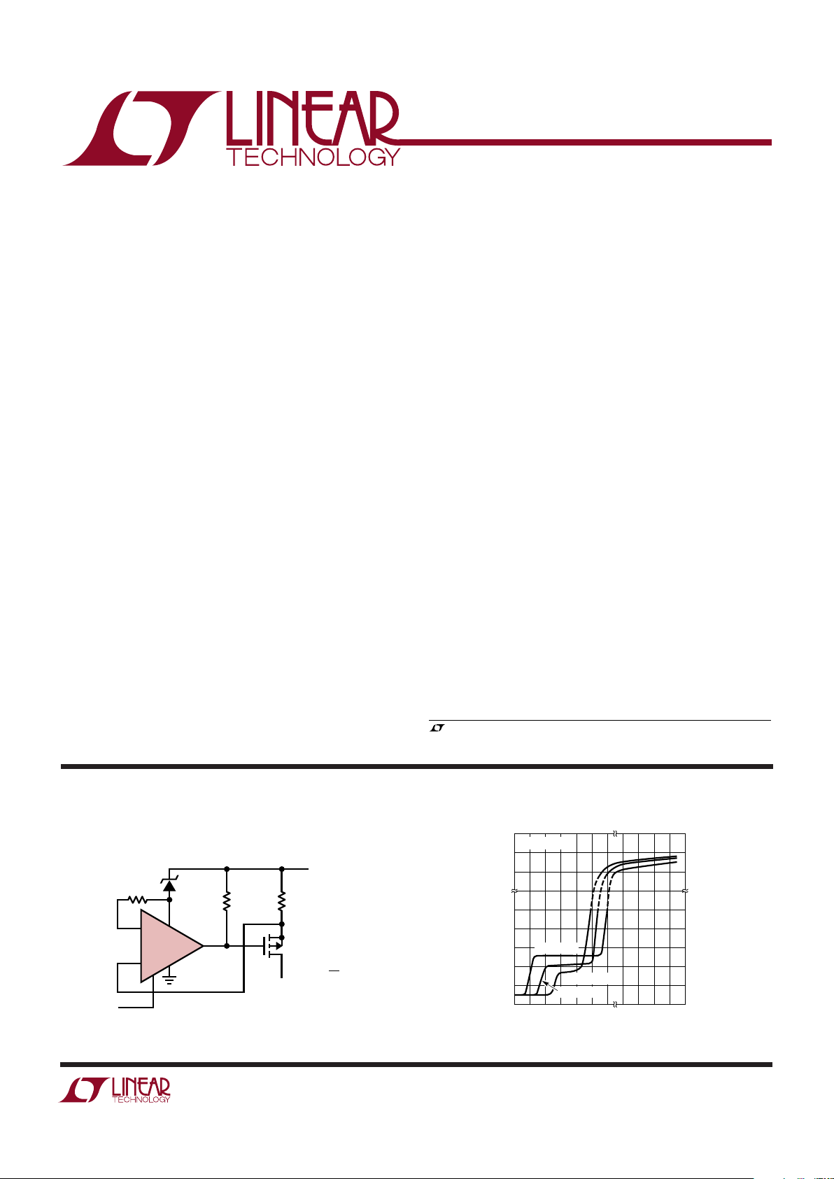
COMMON MODE VOLTAGE (V)
4.0
–10
INPUT BIAS CURRENT (nA)
0
20
30
40
5.210203040
5000
1636 G03
10
4.4 4.8 50
1000
3000
VS = 5V, 0V
TA = –55°C
T
A
= 125°C
TA = 25°C
Input Bias Current vs Common Mode Voltage
Over-The-Top Current Source with Shutdown
SHDN
I
OUT
LT1004-1.2
1M
*OPTIONAL FOR LOW OUTPUT CURRENTS
4V TO
44V
R
TPO610
1636 TA01
R*
–
+
LT1636
I
OUT
=
e.g., 10mA = 120Ω
1.2
R
■
Battery- or Solar-Powered Systems
Portable Instrumentation
Sensor Conditioning
■
Supply Current Sensing
■
Battery Monitoring
■
MUX Amplifiers
■
4mA to 20mA Transmitters
FEATURES
DESCRIPTIO
U
APPLICATIO S
U
TYPICAL APPLICATIO
U
2
LT1636
1636fb
ABSOLUTE MAXIMUM RATINGS
W
WW
U
Total Supply Voltage (V+ to V–) .............................. 44V
Input Differential Voltage ......................................... 44V
Input Current ...................................................... ±25mA
Shutdown Pin Voltage Above V–............................. 32V
Shutdown Pin Current ....................................... ±10mA
Output Short-Circuit Duration (Note 2).........Continuous
Operating Temperature Range (Note 3)
LT1636C/LT1636I .............................. – 40°C to 85°C
LT1636H .......................................... – 40°C to 125°C
Specified Temperature Range (Note 4)
LT1636C/LT1636I .............................. – 40°C to 85°C
LT1636H .......................................... – 40°C to 125°C
Junction Temperature........................................... 150°C
Junction Temperature (DD Package) ................... 125°C
Storage Temperature Range ................. –65°C to 150°C
Storage Temperature Range
(DD Package) ....................................... – 65°C to 125°C
Lead Temperature (Soldering, 10 sec).................. 300°C
(Note 1)
ORDER PART
NUMBER
*The temperature grades are identified by a label on the shipping container. Consult factory for parts specified with wider operating temperature ranges.
ORDER PART
NUMBER
S8 PART
MARKING
1636
1636I
1636H
LT1636CN8
LT1636CS8
LT1636IN8
LT1636IS8
LT1636HS8
T
JMAX
= 150°C, θJA = 150°C/W (N8)
T
JMAX
= 150°C, θJA = 190°C/W (S8)
PACKAGE/ORDER I FOR ATIO
UUW
MS8 PART
MARKING
LTCL
LT1636CMS8
T
JMAX
= 150°C, θJA = 250°C/W
ORDER PART
NUMBER
DD PART*
MARKING
LAAJLT1636CDD
LT1636IDD
T
JMAX
= 125°C, θJA = 160°C/W (NOTE 2)
TOP VIEW
DD PACKAGE
8-LEAD (3mm × 3mm) PLASTIC DFN
5
6
7
8
4
3
2
1NULL
–IN
+IN
V
–
NULL
V
+
OUT
SHDN
1
2
3
4
8
7
6
5
TOP VIEW
MS8 PACKAGE
8-LEAD PLASTIC MSOP
NULL
–IN
+IN
V
–
NULL
V
+
OUT
SHDN
1
2
3
4
8
7
6
5
TOP VIEW
NULL
–IN
+IN
V
–
NULL
V
+
OUT
SHDN
N8 PACKAGE
8-LEAD PDIP
S8 PACKAGE
8-LEAD PLASTIC SO
LT1636C/LT1636I
SYMBOL PARAMETER CONDITIONS MIN TYP MAX UNITS
V
OS
Input Offset Voltage N8 Package 50 225 µV
0°C ≤ TA ≤ 70°C ● 400 µV
–40°C ≤ T
A
≤ 85°C ● 550 µV
S8 Package 50 225 µV
0°C ≤ TA ≤ 70°C ● 600 µV
–40°C ≤ T
A
≤ 85°C ● 750 µV
MS8 Package 50 225 µV
0°C ≤ TA ≤ 70°C ● 700 µV
–40°C ≤ T
A
≤ 85°C ● 850 µV
The ● denotes the specifications which apply over the full operating temperature range of –40°C ≤ TA ≤ 85°C.
VS = 3V, 0V; VS = 5V, 0V; VCM = V
OUT
= half supply unless otherwise specified. (Note 4)
3V 5VAUD ELECTRICAL CHARACTERISTICS
UNDERSIDE METAL CONNECTED TO V
–
3
LT1636
1636fb
LT1636C/LT1636I
SYMBOL PARAMETER CONDITIONS MIN TYP MAX UNITS
DD Package 75 425 µV
0°C ≤ T
A
≤ 70°C ● 900 µV
–40°C ≤ TA ≤ 85°C ● 1050 µV
Input Offset Voltage Drift (Note 9) N8 Package, –40°C ≤ TA ≤ 85°C ● 15µV/°C
S8 Package, –40°C ≤ T
A
≤ 85°C ● 28µV/°C
MS8 Package, –40°C ≤ TA ≤ 85°C ● 210µV/°C
DD Package, –40°C ≤ T
A
≤ 85°C ● 210µV/°C
I
OS
Input Offset Current ● 0.1 0.8 nA
VCM = 44V (Note 5) ● 0.6 µA
I
B
Input Bias Current ● 58 nA
V
CM
= 44V (Note 5) ● 36 µA
V
S
= 0V 0.1 nA
Input Noise Voltage 0.1Hz to 10Hz 0.7 µV
P-P
e
n
Input Noise Voltage Density f = 1kHz 52 nV/√Hz
i
n
Input Noise Current Density f = 1kHz 0.035 pA/√Hz
R
IN
Input Resistance Differential 6 10 MΩ
Common Mode, VCM = 0V to 44V 7 15 MΩ
C
IN
Input Capacitance 4pF
Input Voltage Range ● 044V
CMRR Common Mode Rejection Ratio VCM = 0V to VCC – 1V ● 84 110 dB
(Note 5) V
CM
= 0V to 44V (Note 8) ● 86 98 dB
A
VOL
Large-Signal Voltage Gain VS = 3V, VO = 500mV to 2.5V, RL = 10k 200 1300 V/mV
V
S
= 3V, 0°C ≤ TA ≤ 70°C ● 133 V/mV
VS = 3V, –40°C ≤ TA ≤ 85°C ● 100 V/mV
VS = 5V, VO = 500mV to 4.5V, RL = 10k 400 2000 V/mV
V
S
= 5V, 0°C ≤ TA ≤ 70°C ● 250 V/mV
VS = 5V, –40°C ≤ TA ≤ 85°C ● 200 V/mV
V
OL
Output Voltage Swing LOW No Load ● 210 mV
I
SINK
= 5mA ● 480 875 mV
VS = 5V, I
SINK
= 10mA ● 860 1600 mV
V
OH
Output Voltage Swing HIGH VS = 3V, No Load ● 2.95 2.985 V
V
S
= 3V, I
SOURCE
= 5mA ● 2.55 2.8 V
VS = 5V, No Load ● 4.95 4.985 V
VS = 5V, I
SOURCE
= 10mA ● 4.30 4.75 V
I
SC
Short-Circuit Current (Note 2) VS = 3V, Short to GND 7 15 mA
V
S
= 3V, Short to V
CC
20 42 mA
VS = 5V, Short to GND 12 25 mA
V
S
= 5V, Short to V
CC
25 50 mA
PSRR Power Supply Rejection Ratio VS = 2.7V to 12.5V, VCM = VO = 1V ● 90 103 dB
Reverse Supply Voltage IS = –100µA ● 27 40 V
I
S
Supply Current (Note 6) 42 55 µA
● 60 µA
Supply Current, SHDN V
PIN5
= 2V, No Load (Note 6) ● 412 µA
I
SD
Shutdown Pin Current V
PIN5
= 0.3V, No Load (Note 6) ● 0.5 15 nA
V
PIN5
= 2V, No Load (Note 5) ● 1.1 5 µA
Output Leakage Current, SHDN V
PIN5
= 2V, No Load (Note 6) ● 0.05 1 µA
Maximum Shutdown Pin Current V
PIN5
= 32V, No Load (Note 5) ● 27 150 µA
t
ON
Turn-On Time V
PIN5
= 5V to 0V, RL = 10k 120 µs
t
OFF
Turn-Off Time V
PIN5
= 0V to 5V, RL = 10k 2.5 µs
The ● denotes the specifications which apply over the full operating temperature range of –40°C ≤ TA ≤ 85°C.
VS = 3V, 0V; VS = 5V, 0V; VCM = V
OUT
= half supply unless otherwise specified. (Note 4)
3V 5VAUD ELECTRICAL CHARACTERISTICS
4
LT1636
1636fb
The ● denotes the specifications which apply over the full operating temperature range of –40°C ≤ TA ≤ 85°C.
VS = 3V, 0V; VS = 5V, 0V; VCM = V
OUT
= half supply unless otherwise specified. (Note 4)
3V 5VAUD ELECTRICAL CHARACTERISTICS
LT1636C/LT1636I
SYMBOL PARAMETER CONDITIONS MIN TYP MAX UNITS
GBW Gain Bandwidth Product f = 1kHz 110 200 kHz
(Note 5) 0°C ≤ T
A
≤ 70°C ● 100 kHz
–40°C ≤ TA ≤ 85°C ● 90 kHz
SR Slew Rate AV = –1, R
L
= ∞ 0.035 0.07 V/µs
(Note 7) 0°C ≤ T
A
≤ 70°C ● 0.031 V/µs
–40°C ≤ T
A
≤ 85°C ● 0.030 V/µs
LT1636C/LT1636I
SYMBOL PARAMETER CONDITIONS MIN TYP MAX UNITS
V
OS
Input Offset Voltage N8 Package 100 450 µV
0°C ≤ TA ≤ 70°C ● 550 µV
–40°C ≤ T
A
≤ 85°C ● 700 µV
S8 Package 100 450 µV
0°C ≤ TA ≤ 70°C ● 750 µV
–40°C ≤ T
A
≤ 85°C ● 900 µV
MS8 Package 100 450 µV
0°C ≤ TA ≤ 70°C ● 850 µV
–40°C ≤ TA ≤ 85°C ● 1000 µV
DD Package 125 650 µV
0°C ≤ T
A
≤ 70°C ● 1050 µV
–40°C ≤ TA ≤ 85°C ● 1200 µV
Input Offset Voltage Drift (Note 9) N8 Package, –40°C ≤ TA ≤ 85°C ● 1 4µV/°C
S8 Package, –40°C ≤ T
A
≤ 85°C ● 2 8 µV/°C
MS8 Package, –40°C ≤ TA ≤ 85°C ● 210µV/°C
DD Package, –40°C ≤ T
A
≤ 85°C ● 210µV/°C
I
OS
Input Offset Current ● 0.2 1.0 nA
I
B
Input Bias Current ● 410 nA
Input Noise Voltage 0.1Hz to 10Hz 1 µV
P-P
e
n
Input Noise Voltage Density f = 1kHz 52 nV/√Hz
i
n
Input Noise Current Density f = 1kHz 0.035 pA/√Hz
R
IN
Input Resistance Differential 5.2 13 MΩ
Common Mode, VCM = –15V to 14V 12000 MΩ
C
IN
Input Capacitance 4pF
Input Voltage Range ● –15 29 V
CMRR Common Mode Rejection Ratio VCM = –15V to 29V ● 86 103 dB
A
VOL
Large-Signal Voltage Gain VO = ±14V, RL = 10k 100 500 V/mV
0°C ≤ TA ≤ 70°C ● 75 V/mV
–40°C ≤ T
A
≤ 85°C ● 50 V/mV
V
OL
Output Voltage Swing LOW No Load ● –14.997 –14.95 V
I
SINK
= 5mA ● –14.500 –14.07 V
I
SINK
= 10mA ● –14.125 –13.35 V
V
OH
Output Voltage Swing HIGH No Load ● 14.9 14.975 V
I
SOURCE
= 5mA ● 14.5 14.750 V
I
SOURCE
= 10mA ● 14.3 14.650 V
The ● denotes the specifications which apply over the full operating temperature range of –40°C ≤ TA␣ ≤␣85°C.
VS = ±15V, VCM = 0V, V
OUT
= 0V, V
SHDN
= V– unless otherwise specified. (Note 4)
±15V ELECTRICAL CHARACTERISTICS
5
LT1636
1636fb
LT1636C/LT1636I
SYMBOL PARAMETER CONDITIONS MIN TYP MAX UNITS
I
SC
Short-Circuit Current (Note 2) Short to GND ±18 ±30 mA
0°C ≤ T
A
≤ 70°C ● ±15 mA
–40°C ≤ T
A
≤ 85°C ● ±10 mA
PSRR Power Supply Rejection Ratio VS = ±1.35V to ±22V ● 90 114 dB
I
S
Supply Current 50 70 µA
● 85 µA
Positive Supply Current, SHDN V
PIN5
= –20V, VS = ±22V, No Load ● 12 30 µA
I
SHDN
Shutdown Pin Current V
PIN5
= –21.7V, VS = ±22V, No Load ● 0.7 15 nA
V
PIN5
= –20V, VS = ±22V, No Load ● 1.2 8 µA
Maximum Shutdown Pin Current V
PIN5
= 32V, VS = ±22V ● 27 150 µA
Output Leakage Current, SHDN V
PIN5
= –20V, VS = ±22V, No Load ● 0.1 2 µA
GBW Gain Bandwidth Product f = 1kHz 125 220 kHz
0°C ≤ T
A
≤ 70°C ● 110 kHz
–40°C ≤ T
A
≤ 85°C ● 100 kHz
SR Slew Rate AV = –1, R
L
= ∞, VO = ±10V Measured at ±5V 0.0375 0.075 V/µs
0°C ≤ T
A
≤ 70°C ● 0.033 V/µs
–40°C ≤ TA ≤ 85°C ● 0.030 V/µs
The ● denotes the specifications which apply over the full operating temperature range of –40°C ≤ TA␣ ≤␣85°C, otherwise
specifications are at TA = 25°C. VS = ±15V, VCM = 0V, V
OUT
= 0V, V
SHDN
= V– unless otherwise specified. (Note 4)
±15V ELECTRICAL CHARACTERISTICS
LT1636H
SYMBOL PARAMETER CONDITIONS MIN TYP MAX UNITS
V
OS
Input Offset Voltage 50 325 µV
● 3mV
Input Offset Voltage Drift (Note 9) ● 310µV/°C
I
OS
Input Offset Current ● 3nA
V
CM
= 44V (Note 5) ● 1 µA
I
B
Input Bias Current ● 30 nA
VCM = 44V (Note 5) ● 10 µA
Input Voltage Range ● 0.3 44 V
CMRR Common Mode Rejection Ratio VCM = 0.3V to VCC – 1V ● 72 dB
(Note 5) VCM = 0.3V to 44V ● 74 dB
A
VOL
Large-Signal Voltage Gain VS = 3V, VO = 500mV to 2.5V, RL = 10k 200 1300 V/mV
● 20 V/mV
VS = 5V, VO = 500mV to 4.5V, RL = 10k 400 2000 V/mV
● 35 V/mV
V
OL
Output Voltage Swing LOW No Load ● 15 mV
I
SINK
= 2.5mA ● 875 mV
V
OH
Output Voltage Swing HIGH VS = 3V, No Load ● 2.925 V
VS = 3V, I
SOURCE
= 5mA ● 2.35 V
VS = 5V, No Load ● 4.925 V
V
S
= 5V, I
SOURCE
= 10mA ● 4.10 V
PSRR Power Supply Rejection Ratio VS = 2.7V to 12.5V, VCM = VO = 1V ● 80 dB
Minimum Supply Voltage ● 2.7 V
The ● denotes the specifications which apply over the full operating temperature range of –40°C ≤ TA ≤ 125°C.
VS = 3V, 0V; VS = 5V, 0V; VCM = V
OUT
= half supply unless otherwise specified. (Note 4)
3V 5VAUD ELECTRICAL CHARACTERISTICS
 Loading...