

FEATURES
■
Guaranteed Operation at 1.2V
■
Op Amp and Reference on Single Chip
■
Micropower: 130µA Supply Current
■
Industrial Temperature Range SO-8 Packages
■
Rail-to-Rail Output
■
High Output Current: 25mA Min
■
Output Drives 1000pF
■
Capable of Floating Mode Operation
■
Specified for 5V and ±5V Supplies
■
Low Reference Drift: 30ppm/°C
■
Industry Standard LM10 Pinout
U
APPLICATIONS
■
Battery- or Solar-Powered Systems
Portable Instrumentation
Sensor Conditioning
■
Precision Current Regulators
■
Precision Voltage Regulators
■
Battery Level Indicator
■
Thermocouple Transmitter
LT1635
Micropower Rail-to-Rail
Op Amp and Reference
U
DESCRIPTION
The LT®1635 is a new analog building block that includes a
rail-to-rail output op amp, a precision reference and reference
buffer. The device operates from supplies as low as a single
1.2V or up to ± 5V, yet it consumes only 130µA of supply
current.
The input common mode range of the op amp includes
ground and incorporates phase reversal protection to prevent false outputs from occurring when the input is below
the negative supply. The rail-to-rail output stage can swing to
within 15mV of each rail with no load and can swing to within
250mV of each rail while delivering 10mA of output current.
The gain bandwidth of the op amp is 175kHz and it is unitygain stable with up to 1000pF load capacitance.
The 0.2V reference is referred to V– and includes a buffer
amplifier to enhance flexibility. The reference and buffer
combine to achieve a drift of 30ppm/°C, a line regulation of
20ppm/V and a load regulation of 150ppm/mA.
The LT1635 is available in 8-pin PDIP and SO packages, and
has the industry standard LM10 pinout.
, LTC and LT are registered trademarks of Linear Technology Corporation.
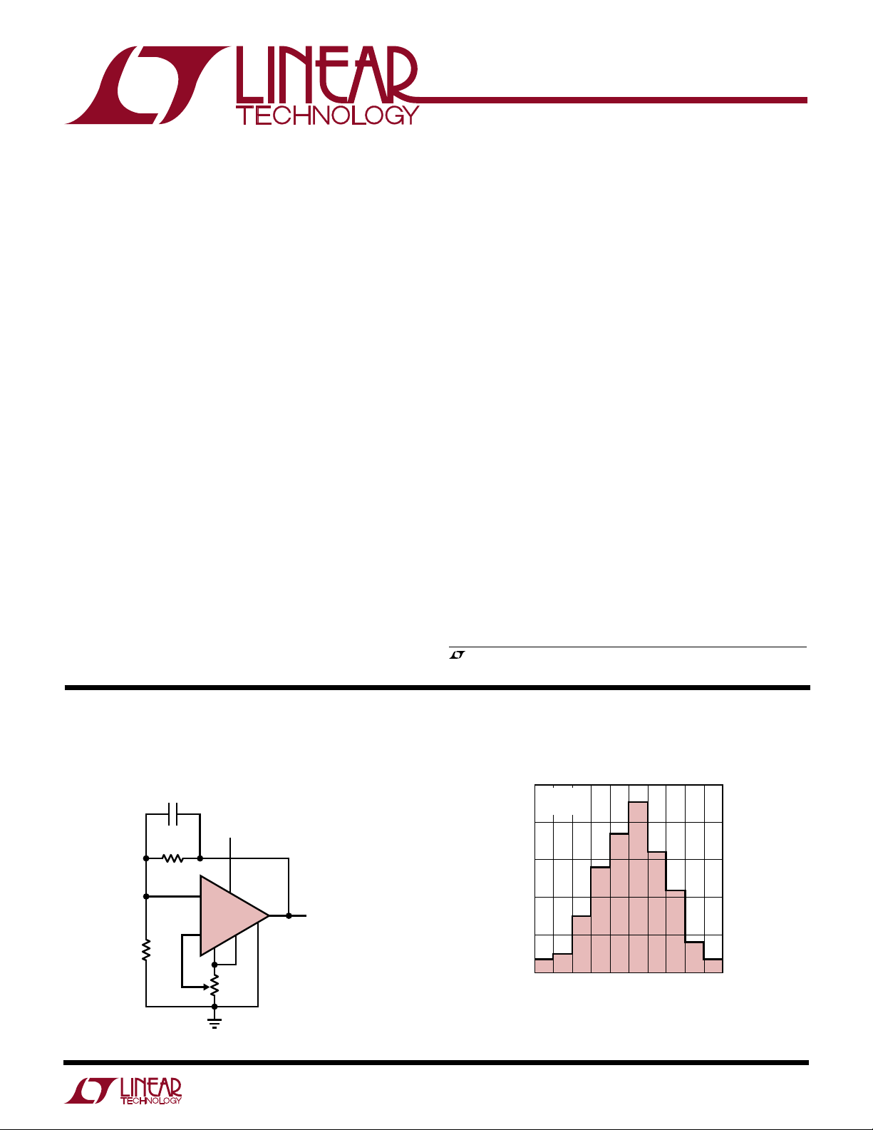
TYPICAL APPLICATION
0V to 5V Regulator
C1
0.01µF
V
> 5.2V
IN
–
7
2
LT1635
+
3
1
R3
5k
6
4
8
1635 TA01
R2
3.9k
V
100k
OUT
ADJ
R1
U
V
OUT
0V TO 5V
Typical Distribution of Input Offset Voltage
25
VS = 5V, 0V
= 25°C
T
A
20
15
10
PERCENT OF UNITS
5
0
–1.0
–0.6
INPUT OFFSET VOLTAGE (mV)
–0.2
0.2
0.6
1.0
1635 TA02
1
LT1635
WW
W
ABSOLUTE MAXIMUM RATINGS
Total Supply Voltage (V+ to V–) .............................. 14V
Input Differential Voltage ......................................... 14V
Input Current ...................................................... ±25mA
Output Short-Circuit Duration .......................Continuous
Operating Temperature Range
(Note 1) .............................................. –40°C to 85°C
Junction Temperature........................................... 150°C
Storage Temperature Range ................. –65°C to 150°C
Lead Temperature (Soldering, 10 sec).................. 300°C
U
U
W
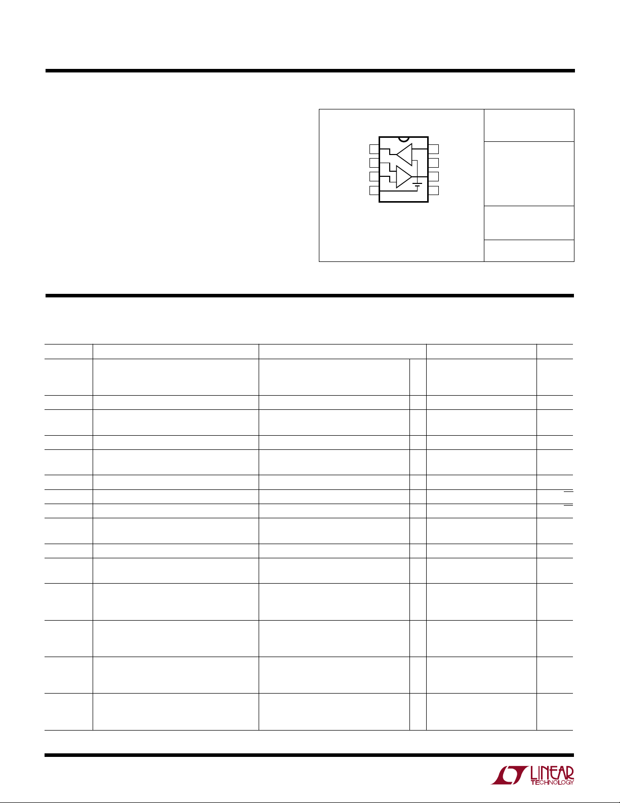
PACKAGE/ORDER INFORMATION
ORDER PART
NUMBER
LT1635CN8
LT1635CS8
LT1635IN8
LT1635IS8
S8 PART
MARKING
REFOUT
OP AMP IN (–)
OP AMP IN (+)
N8 PACKAGE
8-LEAD PDIP
T
JMAX
T
JMAX
TOP VIEW
1
2
3
–
4
V
= 150°C, θJA = 130°C/ W (N8)
= 150°C, θJA = 190°C/ W (S8)
–
+
–
+
+
S8 PACKAGE
8-LEAD PLASTIC SO
REF FB
8
+
V
7
OP AMP OUT
6
BALANCE
5
U
1635 1635I
Consult factory for Military grade parts.
ELECTRICAL CHARACTERISTICS
5V OP AMP: V
SYMBOL PARAMETER CONDITIONS MIN TYP MAX UNITS
V
OS
VOS ADJ Offset Voltage Adjust Range Positive Adjust ● 6 8 mV
I
OS
I
B
e
n
i
n
R
IN
CMRR Common Mode Rejection Ratio VCM = 0V to 4V 92 110 dB
A
VOL
V
OL
V
OH
= 5V, 0V; VCM = V
S
Input Offset Voltage 0.3 1.3 mV
Input Offset Voltage Drift –40°C ≤ TA ≤ 85°C (Note 3) ● 3.0 7.0 µV/°C
Input Offset Current ● 0.2 0.6 nA
Input Bias Current 2.0 4.0 nA
Input Noise Voltage 0.1Hz to 10Hz 1 µV
Input Noise Voltage Density f = 1kHz 50 nV/√Hz
Input Noise Current Density f = 1kHz 0.05 pA/√Hz
Input Resistance Differential ● 725 MΩ
Input Voltage Range ● 04V
Large-Signal Voltage Gain VO = 200mV to 4.5V, No Load ● 100 450 V/mV
Shunt Gain I
Output Voltage Swing Low VS = 5V, No Load ● 210 mV
Output Voltage Swing High VS = 5V, No Load ● 4.975 4.985 V
= 2.5V, TA = 25°C, unless otherwise noted. (Note 1)
OUT
0°C ≤ TA ≤ 70°C ● 0.5 1.6 mV
–40°C ≤ T
Negative Adjust
Common Mode, VCM = 0V to 4V 6 GΩ
V
O
V
O
OUT
V
O
(Note 4) ● 8 20 V/mV
V
S
V
S
V
S
V
S
≤ 85°C ● 1.8 mV
A
= 200mV to 4.5V, RL = 1.1k ● 45 200 V/mV
= 200mV to 4.5V, RL = 500Ω ● 35 150 V/mV
= 0.1mA to 5mA V/mV
= 1.5V to 6.45V 15 25 V/mV
= 5V, I
= 5V, I
= 5V, I
= 5V, I
= 5mA ● 125 250 mV
SINK
= 10mA ● 200 500 mV
SINK
= 5mA ● 4.65 4.8 V
SOURCE
= 10mA ● 4.55 4.75 V
SOURCE
● –1.4 – 2 mV
● 2.5 5.0 nA
P-P
● 85 97 dB
2
ELECTRICAL CHARACTERISTICS
LT1635
5V OP AMP: V
SYMBOL PARAMETER CONDITIONS MIN TYP MAX UNITS
I
SC
PSRR Power Supply Rejection Ratio VS = 1.2V to 12V, VCM = VO = 0.2V 93 100 dB
I
S
GBW Gain Bandwidth Product f = 1kHz 175 kHz
SR Slew Rate AV = –1, R
5V REFERENCE: V
SYMBOL PARAMETER CONDITIONS MIN TYP MAX UNITS
V
REF
TC V
REF
= 5V, 0V; VCM = V
S
Short-Circuit Current VS = 5V, Short to GND ● 25 40 mA
Minimum Operating Supply Voltage (Note 2) ● 1.1 1.2 V
Supply Current 130 200 µA
= 5V, 0V; TA = 25°C, unless otherwise noted. (Note 1)
S
Feedback Sense Voltage Voltage at Pin 1 with Pin 1 Connected ● 189 200 211 mV
Reference Drift (Note 3) ● 30 100 ppm/°C
Feedback Current Current into Pin 8 3.5 10 nA
Line Regulation 0 ≤ I
Load Regulation I
Reference Amplifier Gain VO = 0.2V to 3.5V 45 90 V/mV
= 2.5V, TA = 25°C, unless otherwise noted. (Note 1)
OUT
= 5V, Short to V
V
S
to Pin 8 (Note 5)
≤ 1mA, V
REF
= 1.2V to 5V 20 35 ppm/V
V
S
= 1.3V to 5V (Note 2) ● 30 55 ppm/ V
V
S
= 0 to 1mA 150 300 ppm/mA
REF
CC
= ∞ 0.045 V/µs
L
= 200mV
REF
● 25 40 mA
● 90 97 dB
● 150 260 µA
● 5.0 15 nA
● 200 500 ppm/mA
● 25 50 V/mV
±5V OP AMP: V
SYMBOL PARAMETER CONDITIONS MIN TYP MAX UNITS
V
OS
VOS ADJ Offset Voltage Adjust Range Positive Adjust ● 6 8 mV
I
OS
I
B
e
n
i
n
R
IN
CMRR Common Mode Rejection Ratio VCM = –5V to 4V 94 115 dB
= ±5V; VCM = V
S
Input Offset Voltage 0.3 1.5 mV
Input Offset Voltage Drift 0°C ≤ TA ≤ 85°C (Note 3) ● 4.5 10.0 µV/°C
Input Offset Current ● 0.2 0.6 nA
Input Bias Current 2.0 4 nA
Input Noise Voltage 0.1Hz to 10Hz 1 µV
Input Noise Voltage Density f = 1kHz 50 nV/√Hz
Input Noise Current Density f = 1kHz 0.05 pA/√Hz
Input Resistance Differential ● 735 MΩ
Input Voltage Range ● –5 4 V
= 0V, TA = 25°C, unless otherwise noted. (Note 1)
OUT
≤ 70°C ● 0.5 1.9 mV
0°C ≤ T
A
–40°C ≤ TA ≤ 85°C ● 2.1 mV
Negative Adjust ● –1.4 –2 mV
Common Mode, V
= –5V to 4V 9 GΩ
CM
● 2.5 5 nA
P-P
● 91 110 dB
3
LT1635
ELECTRICAL CHARACTERISTICS
±5V OP AMP: V
SYMBOL PARAMETER CONDITIONS MIN TYP MAX UNITS
A
VOL
V
O
I
SC
PSRR Power Supply Rejection Ratio VS = ±1V to ±6V, VCM = VO = 0V 90 100 dB
I
S
GBW Gain Bandwidth Product f = 1kHz 175 kHz
SR Slew Rate AV = –1, R
±5V REFERENCE: V
SYMBOL PARAMETER CONDITIONS MIN TYP MAX UNITS
V
REF
TC V
REF
= ±5V; VCM = V
S
Large-Signal Voltage Gain VO = –4.5V to 4.5V, No Load ● 175 300 V/mV
Output Voltage Swing VS = ±5V, No Load ● ±4.975 ±4.985 mV
Short-Circuit Current VS = ±5V ±25 ±40 mA
Supply Current 135 215 µA
= ±5V, TA = 25°C, unless otherwise noted. (Note 1)
S
Feedback Sense Voltage Voltage at Pin 1 with Pin 1 Connected ● 189 200 211 mV
Reference Drift (Note 3) ● 40 120 ppm/°C
Feedback Current Current into Pin 8 3.5 10 nA
Line Regulation 0 ≤ I
Load Regulation I
Reference Amplifier Gain VO = 0.2V to 8.5V 45 90 V/mV
= 0V, TA = 25°C, unless otherwise noted. (Note 1)
OUT
V
= –4.5V to 4.5V, RL = 1.1k ● 15 100 V/mV
O
V
= –4.5V to 4.5V, RL = 500Ω ● 10 60 V/mV
O
V
= ±5V, I
S
V
= ±5V, I
S
to Pin 8 (Note 5)
REF
V
= ±0.6V to ±5V 20 25 ppm /V
S
= ±0.65V to ±5V (Note 2) ● 30 55 ppm/V
V
S
= 0 to 1mA 150 300 ppm/mA
REF
VS = 10V, 0V ● 25 50 V/mV
= 5mA ● ±4.65 ±4.75 mV
SINK
= 10mA ● ±4.5 ±4.6 mV
SINK
= ∞ 0.05 V/µs
L
≤ 1mA, V
= 200mV
REF
● 88 98 dB
● 160 280 µA
● 5.0 15 nA
● 200 500 ppm/mA
The ● denotes specifications that apply over the full operating temperature
range.
Note 1: The LT1635C is guaranteed to operate over the commercial
temperature range of 0°C to 70°C. It is designed, characterized and
expected to meet these extended temperature limits, but is not tested at
–40°C and 85°C. The LT1635I is guaranteed to meet the industrial
temperature range.
Note 2: The LT1635 op amp operates on a 1.2V supply over the full
industrial temperature range with an input common mode of 0V to 0.2V.
The minimum supply voltage for the reference to operate properly over
this temperature range is 1.3V.
4
Note 3: This parameter is not 100% tested. Temperature coefficient is
measured by dividing the change in output voltage by specified
temperature range.
Note 4: Shunt gain defines the operation in floating applications when the
output is connected to the V
referred to V
Note 5: If part is stored outside of the specified temperature range, the
output may shift due to hysteresis.
–
.
+
terminal and input common mode is

UW
COMMON MODE VOLTAGE (V)
–1
INPUT BIAS CURRENT (nA)
–2
–1
0
3
1635 G03
–3
–4
–5
0
1
2
4
TA = 125°C
VS = 5V, 0V
TA = 25°C
TA = –55°C
TIME AFTER POWER ON (MINUTES)
0
0
CHANGE IN OFFSET VOLTAGE (µV)
20
60
80
100
140
1
5
7
1635 G09
40
120
4
9
10
2
3
68
V
S
= ±5V
T
A
= 25°C
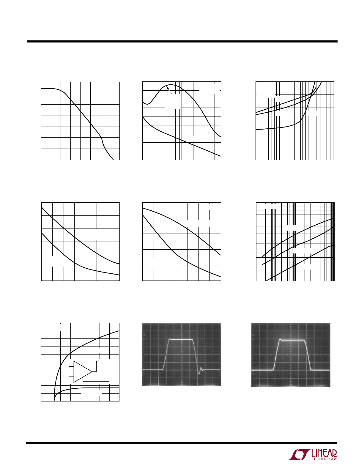
TYPICAL PERFORMANCE CHARACTERISTICS
LT1635
Op Amp
Supply Current vs Supply Voltage
220
200
180
160
140
120
SUPPLY CURRENT (µA)
100
80
60
TA = –55°C
= 25°C
T
A
T
= 125°C
A
6
2
3
4
5
SUPPLY VOLTAGE (V)
7
0.1Hz to 10Hz Noise Voltage
VS = ±5V
= 25°C
T
A
Input Bias and Offset Currents
vs Temperature
100
I
50
0
OFFSET CURRENT (pA)BIAS CURRENT (nA)
–1
–2
10
8
9
1635 G01
–3
–50
–25
OS
I
B
25
0
TEMPERATURE (°C)
50
VS = 5V, 0V
75
100
125
1635 G02
Input Bias Current
vs Common Mode Voltage
Noise Voltage Density
vs Frequency
80
VS = ±2.5V
= 25°C
T
A
70
60
Input Noise Current vs Frequency
0.5
VS = ±2.5V
= 25°C
T
A
0.4
0.3
NOISE VOLTAGE (1µV/DIV)
0
Typical Distribution of Offset
Voltage Drift with Temperature
25
VS = 5V, 0V
20
15
10
PERCENT OF UNITS
5
0
–6
1
–4
2
6
5
4
3
TIME (SEC)
–2 0 2
TCVOS (µV/°C)
7
89
10
1635 G04
46
1635 G07
50
40
INPUT NOISE VOLTAGE DENSITY (nV/√Hz)
30
1
10 100 1000
FREQUENCY (Hz)
Minimum Supply Voltage
200
0
–200
–400
–600
–800
CHANGE IN INPUT OFFSET VOLTAGE (V)
–1000
0
TA = 125°C
= 25°C
T
A
T
= –55°C
A
TOTAL SUPPLY VOLTAGE (V)
12
1635 G05
1635 G08
0.2
0.1
INPUT NOISE CURRENT DENSITY (pA/√Hz)
0
1
10 100 1000
FREQUENCY (Hz)
Turn-On Drift
of Three Typical Units
1635 G06
5
LT1635
UW
TYPICAL PERFORMANCE CHARACTERISTICS
Op Amp
Voltage Gain vs Frequency Capacitive Load Handling
120
100
80
60
40
VOLTAGE GAIN (dB)
20
0
–20
0.1 100k
0.01
1 100
10 1k 1M
FREQUENCY (Hz)
VS = ±2.5V
= 25°C
T
A
10k
1635 G10
Gain Phase vs Frequency
60
50
40
30
20
10
0
VOLTAGE GAIN (dB)
–10
–20
–30
10
PHASE
MARGIN
70°
FREQUENCY (kHz)
VS = ±2.5V
= 25°C
T
A
PHASE
GAIN
100 1000
1635 G11
100
120
140
PHASE SHIFT (DEG)
160
180
200
220
240
260
280
60
VS = ±5V
=
∞
R
L
TA = 25°C
50
40
30
OVERSHOOT (%)
20
10
0
10
AV = 5
= 10 AV = 1
A
V
100 1000 10000
CAPACITIVE LOAD (pF)
Gain-Bandwidth Product and
Slew Rate vs Temperature
0.10
0.09
0.08
0.07
0.06
SLEW RATE (V/µs)
0.05
RISING
SLEW RATE
FALLING
SLEW RATE
VS = ±5V
Phase Margin vs Temperature
350
300
250
200
GAIN-BANDWIDTH
150
GAIN-BANDWIDTH PRODUCT (kHz)
PRODUCT
PHASE MARGIN
VS = ±2.5V
75
70
PHASE MARGIN (DEG)
65
60
55
Voltage Gain vs Load Resistance
1M
VS = 5V, 0V
TA = –55°C
VOLTAGE GAIN (V/V)
1635 G12
TA = 25°C
TA = 125°C
0.04
–50
–25 0
25 75
TEMPERATURE (°C)
Shunt Gain
0.5
T
= 25°C
A
0.4
0.3
0.2
0.1
INPUT VOLTAGE CHANGE (mV)
0
0
13
+
V
IN
–
2
OUTPUT VOLTAGE (V)
50 100 125
I
= 20mA
OUT
V
I
OUT
I
= 1mA
OUT
7
5
6
4
1635 G13
+
OUT
–
1635 G16
100
8
–50 –25
0
TEMPERATURE (°C)
50
25
75
100
1635 G14
Large-Signal Transient Response
VS = ±5V
2V/DIV
1635 G17
A
= 1, NO LOAD
V
INPUT 8V
200µs/DIV
P-P
125
50
100k
0.1
LOAD RESISTANCE TO GROUND (kΩ)
10 1001 1000
1635 G15
Large-Signal Transient Response
VS = 5V, 0V
0V
1V/DIV
A
= 1, NO LOAD
V
INPUT PULSE 0V TO 4V
100µs/DIV
0V
1635 G18
6

UW
SOURCING LOAD CURRENT (mA)
0.001
0.01
OUTPUT SATURATION VOLTAGE (V)
0.1
1
0.10.01 101
1635 G21
VS = ±2.5V
V
OD
= 30mV
TA = 125°C
TA = –55°C
TA = 25°C
FREQUENCY (Hz)
0.1
0
POWER SUPPLY REJECTION RATIO (dB)
20
40
60
80
120
1
10 100 1k
1635 G24
10k 100k
100
VS = ±2.5V
T
A
= 25°C
POSITIVE
SUPPLY
NEGATIVE
SUPPLY
TYPICAL PERFORMANCE CHARACTERISTICS
LT1635
Op Amp
Output Saturation Voltage
vs Input Overdrive
16
14
12
10
8
6
4
2
OUTPUT SATURATION VOLTAGE (mV)
0
510 20
0
INPUT OVERDRIVE (mV)
V
= ±2.5V, NO LOAD
S
= 25°C
T
A
OUTPUT HIGH
OUTPUT LOW
15
Common Mode Range
vs Temperature
+
V
V+ – 0.5
+
V
– 1
Output Saturation Voltage
vs Load Current (Output Low)
1000
VS = ±2.5V
= 30mV
V
OD
100
10
OUTPUT SATURATION VOLTAGE (mV)
25
30
1635 G19
1
0.001 0.1 1 10
0.01
SINKING LOAD CURRENT (mA)
T
= 125°C
A
TA = 25°C
TA = –55°C
1635 G20
Common Mode Rejection Ratio
vs Frequency
120
100
80
VS = ±2.5V
= 25°C
T
A
Output Saturation Voltage
vs Load Current (Output High)
Power Supply Rejection Ratio
vs Frequency
–
V
COMMON MODE RANGE (V)
–
V
– 0.5
–
V
– 1
–50
–25 0
Output Impedance vs Frequency
10000
VS = ±2.5V
= 25°C
T
A
AV = 100
1000
AV = 10 AV = 1
100
10
OUTPUT IMPEDANCE (Ω)
1
0.1 1
FREQUENCY (kHz)
50 100 125
25 75
TEMPERATURE (°C)
10 100 1000
1635 G22
1635 G25
60
40
20
COMMON MODE REJECTION RATIO (dB)
0
1
10 100 1k 10k
FREQUENCY (Hz)
Small-Signal Transient Response
VS = ±5V
10mV/DIV
A
V
C
L
= 1
= 15pF
50µs/DIV
1635 G26
1635 G23
100k
0V
Small-Signal Transient Response
VS = 5V, 0V
10mV/DIV
A
= 1
V
C
= 15pF
L
INPUT 50mV TO 100mV
50µs/DIV
1635 G27
7

LT1635
FREQUENCY (Hz)
1
GAIN (dB)
100
1k
1635 G33
40
0
10 100 10k
–20
–40
120
80
60
20
100k 1M 10M
VS = 5V, 0V
T
A
= 25°C
UW
TYPICAL PERFORMANCE CHARACTERISTICS
Typical Distribution
of Initial Accuracy
20
VS = 5V, 0V
18
= 25°C
T
A
16
14
12
10
8
PERCENT OF UNITS
6
4
2
0
194
196
REFERENCE VOLTAGE (mV)
198
200 202
204
206
1635 G28
Line Regulation
208
VS = 5V, 0V
207
206
205
204
203
202
REFERENCE OUTPUT (mV)
201
200
0
TA = –55°C
TA = 125°C
24 8
SUPPLY VOLTAGE (V)
TA = 25°C
6
10 12 14
Reference
1635 G29
Load Regulation
200
VS = 5V, 0V
= 25°C
T
A
0
–200
–400
REFERENCE CHANGE (ppm)
–600
0
1
SOURCING CURRENT (mA)
2
3
4
1635 G30
Reference Output vs Temperature
of Two Typical Units
205
VS = ±5V
204
203
202
REFERENCE OUTPUT (mV)
201
–50
050
–25 25 75 125
TEMPERATURE (°C)
BLOCK DIAGRA
100
W
1635 G31
2
3
BALANCE
5
–
OP AMPINPUTS
+
Output Saturation
vs Load Current (Sourcing)
1.5
VS = 5V, 0V
1.4
1.3
1.2
1.1
1.0
0.9
0.8
0.7
OUTPUT SATURATION VOLTAGE (V)
0.6
0.5
0
= –55°C
T
A
1
SOURCING CURRENT (mA)
REFERENCE
OUTPUT
FEEDBACK
6
200mV
REFERENCE
TA = 125°C
8
+
TA = 25°C
2
–
REF AMP
+
1635 G32
V
7
4
V
Reference Amplifier Gain
3
+
1
REFERENCE
OUTPUT
–
1635 BD
8

LT1635
–
+
LT1635
OP AMP
5V
99R
(a) (b)
1mV
100mV
R
–
+
5V
1mV
1635 F02
OUTPUT
SATURATED
≈2mV
LT1635
OP AMP
U
WUU
APPLICATIONS INFORMATION
The LT1635 is fully specified with V+ = 5V, V– = 0V and
VCM = 2.5V. The op amp offset voltage is internally
trimmed to a minimum value at these supply voltages. A
unique feature of this device is that it operates from a
single 1.2V supply up to ±5V. A full set of specifications is
provided at ±5V supply voltages. The positive supply pin
of the LT1635 should be bypassed with a small capacitor
(about 0.1µF), as well as the negative supply pin when
using split supplies.
Op Amp
The LT1635 is fully specified for single supply operation,
i.e., when the negative supply is 0V. Input common mode
range of the op amp includes ground and the output
swings within a few millivolts of ground while sinking
current. The input stage of the op amp incorporates phase
reversal protection to prevent false outputs from occurring when the input is below the negative supply. Protective resistors have been included in the input leads so that
current does not become excessive when the inputs are
forced below the negative supply.
The op amp also includes an offset nulling feature, this is
accomplished by connecting the BALANCE pin (Pin 5) to
a variable voltage derived from the reference output. The
offset adjust range is asymmetrical, typically –2mV to
8mV. At room temperature the input offset voltage of the
LT1635 is within the null range, thus the offset voltage can
be adjusted to zero. Figure 1 shows the standard offset
adjustment.
+
V
–
2
3
Figure 1. Standard Offset Adjustment
Output
The output voltage swing of the LT1635 is a function of
input overdrive as shown in the typical performance curves.
When monitoring voltages within 15mV of either rail, gain
LT1635
+
5
1
8
4
R1
10k
6
V
REF
–
V
1635 F01
should be taken to keep the output from saturating. For
example, a 1mV input signal will cause the amplifier to set
up in its linear region in the gain 100 configuration as
shown in Figure 2a. However, 1mV is not enough to make
the amplifier function properly in the voltage follower mode
(Figure 2b).
Figure 2. Gain 100 Amplifier and Voltage Follower
Distortion
There are two main contributors of distortion in op amps:
distortion caused by nonlinear common mode rejection
and output crossover distortion as the output transitions
from sourcing to sinking current. The common mode
rejection ratio of the LT1635 is very good, typically 110dB.
Therefore, as long as the input operates in normal common mode range, there will be very little common mode
induced distortion. Crossover distortion will increase as
the output load resistance decreases. For the lowest distortion, the LT1635 should be operated with the output
always sourcing current.
Reference
The reference of the LT1635 consists of a 200mV precision
bandgap and a reference amplifier. As shown in the block
diagram, the 0.2V precision bandgap is referred to V– and
is internally connected to the noninverting input of the reference amplifier. This configuration offers great flexibility
in that the reference voltage can be amplified or the reference
amplifier can be used as a comparator. Unlike the op amp,
the output of the reference amplifier can only swing within
0.8V (typ) of the positive rail. To guarantee that the reference
amplifier does not saturate over the industrial temperature
range, the minimum operating supply should be 1.3V. The
reference amplifier can source 2mA of load current and can
sink 10µ A over the industrial temperature range.
9

LT1635
1
3
1635 TA08
2D1
8
4
7
6
+
–
LED DIMS BELOW 7V
R2
12k
R3
680k
R1
680k
R4
1.5k
–
+
LT1635
U
TYPICAL APPLICATIONS
Low Voltage Regulator
C1
0.01µF
V
R1
28k
R2
2k
*USE ELECTROLYTIC
OUTPUT CAPACITORS
>3.2V
IN
2
–
7
LT1635
3
+
8
1
6
4
V
OUT
3V
+
OPTIONAL*
1635 TA03
Best Regulation
2
–
LT1635
3
+
R2
48k
2-Terminal Current Regulator Shunt Regulator
+
(R2 + R3)V
I
=
OUT
(R1)(R3)
2
–
7
LT1635
3
+
R1
R2
8
6
4
1
R3
–
1635 TA05
REF
C1*
0.01µF
R2
2
–
LT1635
3
R1
*REQUIRED FOR CAPACITIVE LOADING
+
8
> 6V
V
IN
7
6
V
OUT
4
8
1
R1
2k
7
6
4
1
5V
1635 TA04
+
=V
V
OUT
R2
1 +
REF
()
R1
–
1635 TA06
10
R2
49.9k
1%
2
3
Q1
2N3904
Negative Regulator 6V Battery-Level Indicator
GROUND
+
C1
–
LT1635
+
7
6
4
8
1
R1
2k
1%
47µF
ELECT
V
OUT
–5V
V
IN
≤ –5.5V
1635 TA07

SI PLIFIED
R1
6k
2
R2
INPUTS
6k
3
300k
5
BALANCE
WW
SCHEMATICS
Q1
Q2
Q4
Q3
Q5
LT1635
Op Amp
+
V
7
Q21
Q28
C2
Q15
Q13
Q7
Q6
Q14
Q16
+
C1
Q20
Q17 Q18
Q19
Q26
Q24
Q27
1635 SSOA
Q25
6
4
OUTPUT
–
V
+
7
V
–
V
4
PACKAGE DESCRIPTION
0.300 – 0.325
(7.620 – 8.255)
Reference
REF FB
8 REFOUT
×16
×1
1635 SSREF
1
U
Dimensions in inches (millimeters) unless otherwise noted.
N8 Package
8-Lead PDIP (Narrow 0.300)
(LTC DWG # 05-08-1510)
0.045 – 0.065
(1.143 – 1.651)
0.130 ± 0.005
(3.302 ± 0.127)
876
0.400*
(10.160)
MAX
5
0.065
(1.651)
0.009 – 0.015
(0.229 – 0.381)
+0.025
0.325
–0.015
+0.635
8.255
()
–0.381
*THESE DIMENSIONS DO NOT INCLUDE MOLD FLASH OR PROTRUSIONS.
MOLD FLASH OR PROTRUSIONS SHALL NOT EXCEED 0.010 INCH (0.254mm)
TYP
0.005
(0.127)
MIN
0.100 ± 0.010
(2.540 ± 0.254)
Information furnished by Linear Technology Corporation is believed to be accurate and reliable.
However, no responsibility is assumed for its use. Linear Technology Corporation makes no representation that the interconnection of its circuits as described herein will not infringe on existing patent rights.
0.125
(3.175)
MIN
0.018 ± 0.003
(0.457 ± 0.076)
0.015
(0.380)
MIN
0.255 ± 0.015*
(6.477 ± 0.381)
12
3
4
N8 0695
11

LT1635
TYPICAL APPLICATION
U
1A Shunt Battery Charger (I
1A
SOLAR
ARRAY
*DALE HLM-10
200mV
8
PACKAGE DESCRIPTION
+
LT1635
REF
–
= 230µA, V
DARK
1M
220Ω3
7
+
LT1635
7V
1
68k
2k
2
1M
OP AMP
–
4
FLOAT
6
= 14V)
100nF
TIP121
7.5Ω*
10W
U
Dimensions in inches (millimeters) unless otherwise noted.
S8 Package
8-Lead Plastic Small Outline (Narrow 0.150)
(LTC DWG # 05-08-1610)
2A
12V
5A
GELCEL
1635 TA09
0.189 – 0.197*
(4.801 – 5.004)
0.010 – 0.020
(0.254 – 0.508)
0.008 – 0.010
(0.203 – 0.254)
*
DIMENSION DOES NOT INCLUDE MOLD FLASH. MOLD FLASH
SHALL NOT EXCEED 0.006" (0.152mm) PER SIDE
**
DIMENSION DOES NOT INCLUDE INTERLEAD FLASH. INTERLEAD
FLASH SHALL NOT EXCEED 0.010" (0.254mm) PER SIDE
× 45°
0.016 – 0.050
0.406 – 1.270
0.053 – 0.069
(1.346 – 1.752)
0°– 8° TYP
(0.355 – 0.483)
0.014 – 0.019
0.004 – 0.010
(0.101 – 0.254)
0.050
(1.270)
BSC
0.228 – 0.244
(5.791 – 6.197)
7
8
1
2
5
6
0.150 – 0.157**
(3.810 – 3.988)
SO8 0695
3
4
RELATED PARTS
PART NUMBER DESCRIPTION COMMENTS
LT1178/LT1179 Dual/Quad 17µA Max, Single Supply Precision Op Amps 70µV VOS Max and 2.5µV/°C Drift Max, 85kHz GBW, 0.04V/µs
Slew Rate, Input/Output Common Mode Includes Ground
LT1490/LT1491 Dual/Quad Micropower Rail-to-Rail Input and Output Op Amps Single Supply Input Range: –0.4V to 44V, Micropower 50µA
Amplifier, Rail-to-Rail Input and Output, 200kHz GBW
LT2178/LT2179 Dual/Quad 17µA Max, Single Supply Precision Op Amps SO-8 and 14-Lead Standard Pinout, 70µV VOS Max, 85kHz GBW
LT1078/LT1079 Dual/Quad Micropower, Single Supply Precision Op Amps 70µV VOS Max and 0.4µV/°C Drift, 200kHz GBW, 0.07V/µs Slew
Rate, Input/Output Common Mode Includes Ground
LT2078/LT2079 Dual/Quad Micropower, Single Supply Precision Op Amps SO-8 and 14-Lead Standard Pinout, 70µV VOS Max, 200kHz GBW
12
Linear Technolog y Corporation
1630 McCarthy Blvd., Milpitas, CA 95035-7417 ● (408) 432-1900
FAX: (408) 434-0507
●
TELEX: 499-3977 ● www.linear-tech.com
1635f LT/TP 0997 4K • PRINTED IN USA
LINEAR TECHNOLOGY CORPORATION 1997
 Loading...