

FEATURES
LT1619
Low Voltage Current Mode
PWM Controller
U
DESCRIPTIO
■
Wide VIN Range: 1.9V to 18V
■
300kHz Fixed Frequency Current Mode Control
■
1A Rail-to-Rail N-Channel MOSFET Driver
■
Low 53mV Current Limit Threshold Voltage
Improves Efficiency
■
Implements Boost, SEPIC and Flyback Converters
Requiring Low Side Power Transistors
■
Internal Current Sense Amplifier
with Leading Edge Blanking
■
Up to 500kHz External Synchronization
■
Burst Mode® Operation for High Efficiency
at Light Load
■
140µA Quiescent Current
■
15µA Shutdown Current
■
8-Lead MSOP and SO Packages
U
APPLICATIO S
■
3.3V to 5V DC/DC Converters
■
Distributed Power Supplies
■
Isolated Power Supplies
The LT®1619 is a fixed frequency PWM controller for
implementing current mode DC/DC converters with minimum external parts. The LT1619 operates with input
voltages ranging from 1.9V to 18V and is suitable for a
variety of battery-powered and distributed DC/DC converters. The internal rail-to-rail N-channel MOSFET driver
operates either from the input in the nonbootstrapped
mode or from the output in bootstrapped operation. The
driver is designed to drive a low side power transistor in
boost, SEPIC, flyback and other topologies.
Converter efficiency is improved at heavy loads with a
53mV current sense voltage and at light load with Burst
Mode operation. The operating frequency is internally set
at 300kHz. The oscillator can also be synchronized externally up to 500kHz. No load quiescent current is 140µA and
shutdown current is 15µA.
The LT1619 is available in 8-lead MSOP and SO packages.
, LTC and LT are registered trademarks of Linear Technology Corporation.
Burst Mode is a registered trademark of Linear Technology Corporation.
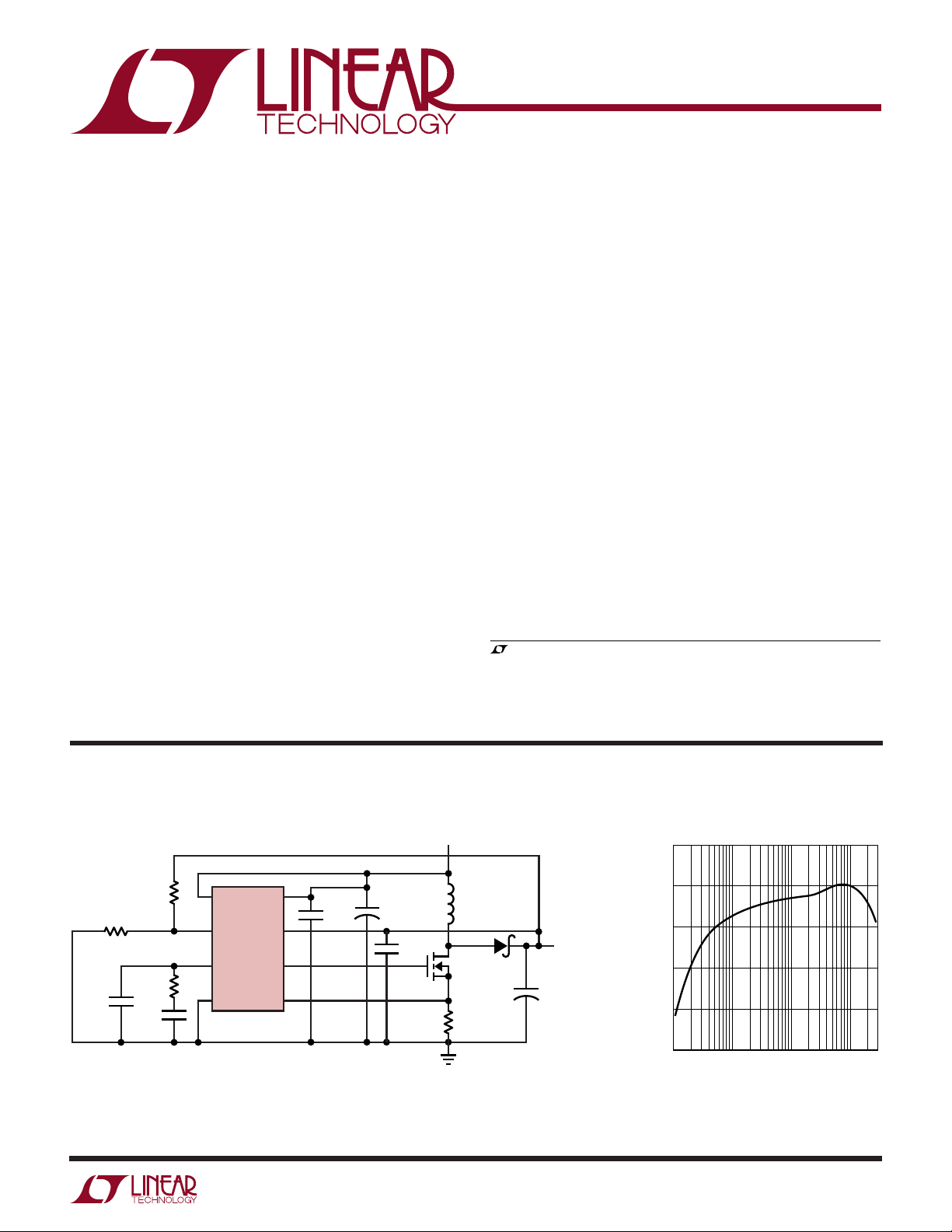
TYPICAL APPLICATIO
37.4k
12.4k
220pF
C1: PANASONIC EEFCDOK220R
: KEMET T495X227K010AS (×2)
C
OUT
D1: MBRD835L
L1: COILCRAFT DO5022P-562
75k
15nF
Figure 1. High Efficiency 3.3V to 5V DC/DC Converter
1
S/S
2
FB
LT1619
3
V
C
4
GND
V
DRV
GATE
SENSE
8
IN
7
6
5
U
0.1µF
V
IN
3.3V
+
C1
22µF
0.1µF
L1
5.6µH
5A
M1
Si9804
R
SENSE
0.01Ω
D1
1619 F01
V
OUT
5V
2.2A
+
C
OUT
440µF
95
90
85
80
EFFICIENCY (%)
75
70
1 100 1000
Efficiency
10
LOAD CURRENT (mA)
1619 F01a
1619fa
1

LT1619
1
2
3
4
8
7
6
5
TOP VIEW
V
IN
DRV
GATE
SENSE
S/S
FB
V
C
GND
S8 PACKAGE
8-LEAD PLASTIC SO
WWWU
ABSOLUTE AXI U RATI GS
(Note 1)
Input Voltage (VIN) ................................... –0.3V to 20V
Gate Drive Supply Voltage (DRV) ............. –0.3V to 20V
Shutdown/Synch Voltage (S/S) ................ –0.3V to 20V
Feedback Voltage (FB) .............................................. V
IN
Compensation Voltage (VC) ...................................... 3V
Gate Drive Output Current (GATE) ........................ ±1.5A
UU
W
PACKAGE/ORDER I FOR ATIO
ORDER PART
NUMBER
TOP VIEW
S/S
1
FB
2
V
3
C
4
GND
MS8 PACKAGE
8-LEAD PLASTIC MSOP
T
= 125°C, θJA = 200°C/W
JMAX
8
7
6
5
V
IN
DRV
GATE
SENSE
LT1619EMS8
MS8 PART MARKING
LTHC
Current Sense Voltage (SENSE) .................– 0.5V to V
IN
Operating Temperature Range (Note 2) .. –40°C to 85°C
Junction Temperature (Note 3)............................. 125°C
Storage Temperature Range ................. –65°C to 150°C
Lead Temperature (Soldering, 10 sec)..................300°C
ORDER PART
NUMBER
LT1619ES8
S8 PART MARKING
1619
= 125°C, θJA = 120°C/W
T
JMAX
Consult LTC Marketing for parts specified with wider operating temperature ranges.
ELECTRICAL CHARACTERISTICS
The ● denotes specifications which apply over the full operating temperature range, otherwise specifications are at TA = 25°C.
V
= V
IN
PARAMETER CONDITIONS MIN TYP MAX UNITS
Reference Voltage Measured at the FB Pin ● 1.22 1.24 1.26 V
Reference Line Regulation 1.9V ≤ VIN ≤ 18V 0.004 0.05 %/V
FB Input Bias Current VFB = V
Error Amplifier Transconductance 80 170 260 µΩ
Error Amplifier Output Source Current VFB = 1V, V
Error Amplifier Output Sink Current VFB = 1.5V, V
Error Amplifier Clamp Voltage VFB = 1V 1.6 2.2 V
Undervoltage Lockout Threshold 1.65 1.85 V
Input Voltage Range ● 1.9 18 V
Switching Frequency 1.9V ≤ VIN ≤ 18V ● 220 300 360 kHz
Synchronization Frequency Range 370 500 kHz
Maximum Duty Cycle ● 88 92 %
Current Limit Threshold ● 40 53 66 mV
Burst Mode Operation Current Limit 10 mV
2
= 2.5V, V
DRV
= VIN, COMP open, V
S/S
= 0V unless otherwise noted.
SENSE
REF
= 1V 4 8.7 14 µA
COMP
= 1V 4 8.7 14 µA
COMP
10 25 nA
–1
1619fa
LT1619
ELECTRICAL CHARACTERISTICS
The ● denotes specifications which apply over the full operating temperature range, otherwise specifications are at TA = 25°C.
V
= V
IN
= 2.5V, V
DRV
PARAMETER CONDITIONS MIN TYP MAX UNITS
Current Sense Input Current V
Current Limit Delay 150 ns
Driver Output Rise Time CL = 3300pF 30 ns
Driver Output Fall Time CL = 3300pF 35 ns
Driver Output High Level I
Driver Output Low Level I
Shutdown Driver Output Level V
Idle Mode Driver Output Level V
S/S Pin Current V
Operating Supply Current VFB = 1V 9 mA
Quiescent Supply Current V
Shutdown Supply Current V
Shutdown Threshold 0.45 1.2 V
Shutdown Delay 12 17 33 µs
= VIN, COMP open, V
S/S
= 0V unless otherwise noted.
SENSE
= 0V ● –90 –120 –150 µA
SENSE
= –20mA V
OUT
I
= –200mA V
OUT
= 20mA 100 200 mV
OUT
= 200mA 0.5 0.7 V
I
OUT
= 0V, I
S/S
= VIN, VFB = 1.5V, I
S/S
= V
S/S
= 0V –2 µA
V
S/S
= VIN, VFB = 1.5V ● 140 220 µA
S/S
= 0V 15 19 µA
S/S
= 0V, VIN = 18V, TA = 85°C40µA
V
S/S
= 20mA 100 200 mV
OUT
= 20mA 100 200 mV
OUT
IN
– 0.6 V
DRV
– 1.6 V
DRV
– 0.35 V
DRV
– 1.2 V
DRV
4 µA
Note 1: Absolute Maximum Ratings are those values beyond which the life
of the device may be impaired.
Note 2: The LT1619E is guaranteed to meet performance specifications
from 0°C to 70°C. Specifications over the –40°C to 85°C operating
Note 3: T
dissipation P
the formula:
is calculated from the ambient temperature TA, the power
J
T
= TA + PD • θ
J
temperature range are assured by design, characterization and correlation
with statistical process controls.
UW
TYPICAL PERFOR A CE CHARACTERISTICS
Bandgap Voltage vs Temperature I
1.245
VIN = 2.5V
1.243
1.241
1.239
1.237
1.235
1.233
1.231
BANDGAP VOLTAGE (V)
1.229
1.227
1.225
–20 0 20 40 60 120
–40
TEMPERATURE (°C)
80 100
1619 G01
(µA)
I
S/S
vs V
S/S
S/S
5
4
3
2
1
0
–1
–2
–3
1.0 2.0 3.0 5.03.50.5 1.5 2.5 4.5
0
TA = –40°C
TA = 25°C
TA = 85°C
V
(V)
S/S
4.0
and the thermal resistance θJA of the package according to
D
JA
S/S Pin Current vs Temperature
5
1619 G02
4
3
2
1
0
S/S PIN CURRENT (µA)
–1
–2
–3
–20
–40
V
= 2.5V
S/S
V
= 0V
S/S
0
40
20
TEMPERATURE (°C)
60
80
100
1619 G03
120
1619fa
3

LT1619
TEMPERATURE (°C)
–40
CURRENT LIMIT THRESHOLD (mV)
57
20
1619 G09
54
52
–20 0 40
51
50
58
56
55
53
60 80 100
VIN = 2.5V
UW
TYPICAL PERFOR A CE CHARACTERISTICS
Shutdown Supply Current
vs Input Voltage
45
40
35
30
25
20
SUPPLY CURRENT (µA)
15
10
5
0
TA = –40°C
TA = 25°C
4 8 12 20142 6 10 18
INPUT VOLTAGE (V)
Maximum Duty Ratio
vs Temperature
95
VIN = 2.5V
94
93
92
DUTY RATIO (%)
91
TA = 85°C
Idle Mode Supply Current
vs Temperature
200
VIN = 2.5V
190
180
170
160
150
IDLE MODE SUPPLY CURRENT (µA)
140
–40
–20 20
16
1619 G04
040
TEMPERATURE (°C)
60
80
100
120
1619 G05
Deviation from Nominal
Frequency vs Input Voltage
8
TA = 25°C
NOMINAL FREQUENCY = 300kHZ
6
4
2
0
FREQUENCY DEVIATION (%)
–2
Frequency Deviation from
Nominal vs Temperature
10
VIN = 2.5V
8
NOMINAL FREQUENCY = 300kHz
6
4
2
0
–2
–4
–6
–8
DEVIATION FROM NOMINAL FREQUENCY (%)
–10
–20 0 40
–40
20
TEMPERATURE (°C)
60 80 100
Current Limit Threshold
vs Temperature
1619 G06
90
–40 –20
Burst Mode Operation Current
Limit Threshold vs Temperature
14
VIN = 2.5V
DUTY CYCLE = 0
12
10
8
6
4
2
CURRENT LIMIT THRESHOLD (mV)
0
–40
–20 0
4
40
20
0
TEMPERATURE (°C)
40 80 100
20 60
TEMPERATURE (°C)
80
100
1619 G07
1619 G10
60
–4
4
2
0
10
8
6
INPUT VOLTAGE (V)
SENSE Pin Input Bias Current
vs Temperature
–115
V
= 0V
SENSE
–117
–119
–121
–123
–125
–127
–129
SENSE PIN CURRENT (µA)
–131
–133
–135
–40
–20
0
20
TEMPERATURE (°C)
16
12
14
18
1619 G08
20
SENSE Pin Input Bias Current
vs Sense Voltage
–90
TA = 25°C
–95
–100
–105
–110
–115
–120
SENSE PIN CURRENT (µA)
–125
40
60
80
100
1619 G11
–130
–10
010
20 30
V
SENSE
(mV)
40 50
60
1619 G12
1619fa

LT1619
U
UU
PI FU CTIO S
S/S (Pin 1): Shutdown and Synchronization. Shutdown is
active low with a typical threshold voltage of 0.9V. For
normal operation, the S/S pin is tied to VIN. To externally
synchronize the controller, drive the S/S pin with pulses.
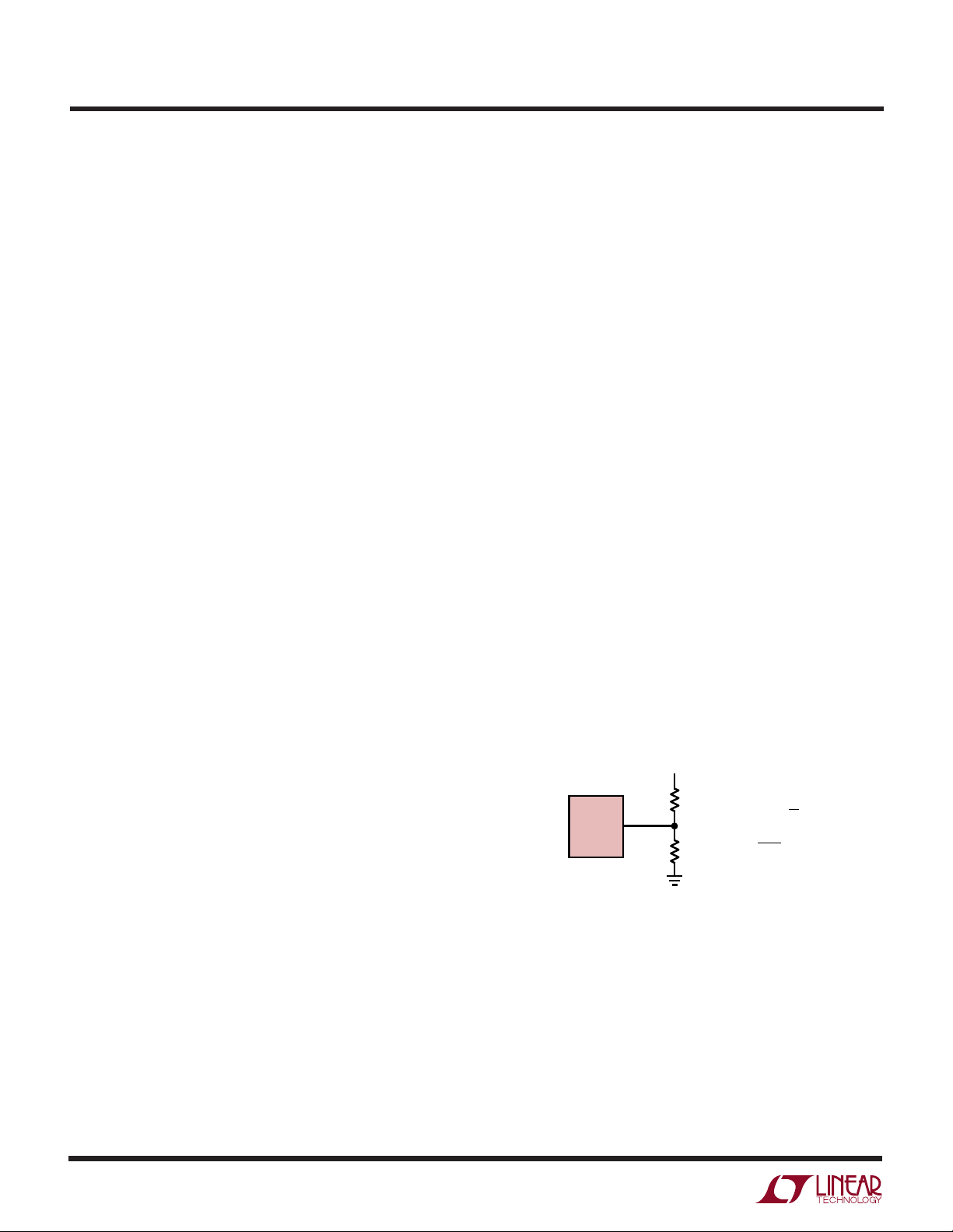
FB (Pin 2): The inverting Input of the Error Amplifier.
Connect the resistor divider tap here. Set V
to V
= 1.24(1 + R1/R2). See Figure 1.
OUT
according
OUT
VC (Pin 3): Compensation Pin for the Error Amplifier. VC is
the output of the transconductance amplifier. Overall loop
is compensated with an RC network from this pin to the
ground.
GND (Pin 4): Ground. Connect to local ground plane.
W
BLOCK DIAGRA
V
CVIN
1.24V
FB
3 8
ERROR
AMPLIFIER
1.8V
+
g
m
2
–
–
A2
UVLO
+
–
A1
V
+
B
–
SENSE (Pin 5): The Input of the Current Sense Amplifier.
The SENSE pin is connected to the source of the N-channel
MOSFET and to a sense resistor to the ground. The current
limit threshold is internally set at 53mV, giving a maximum
switch current of 53mV/R
SENSE
.
GATE (Pin 6): The Output of the MOSFET Driver.
DRV (Pin 7): The Pull-Up Supply of the MOSFET Driver. Tie
this pin to VIN (Pin 8) for nonbootstrapped operation or to
the converter output for bootstrapped operation.
VIN (Pin 8): Supply or Battery Input. Must be closely
bypassed to the ground plane.
IDLE
V
IN
DRV
7
S/S
C1
+
++
Σ
RAMP COMP
DELAY
300kHz
OSCILLATOR
REF/BIAS
1
SYNC
SHUTDOWN
CLK
COMPARATOR
CURRENT
LIMIT
S
Q
R
DRIVER
–
CURRENT
SENSE
+
AMP
+
I
–
LIM
280ns
LEADING
EDGE
BLANKING
6
5
4
GATE
SENSE
GND
1619 F02
R
LOAD
SENSE
Figure 2. LT1619 Block Diagram
1619fa
5
LT1619
OPERATIO
U
The LT1619 is a fixed frequency current mode switching
regulator PWM controller that can be used in boost, SEPIC
or flyback modes. The device operates from an input
supply range of 1.9V to 18V, and has a separate supply pin
(DRV) for the gate driver. The DRV pin can be bootstrapped
to V
for additional gate enhancement in low voltage
OUT
applications like 3.3V to 5V boost converters, or connected to the input supply for higher voltage inputs.
To best understand operation of the LT1619, please refer
to Figure 2, the Block Diagram. The gate drive circuit turns
on the external MOSFET at the trailing edge of oscillator
output signal CLK. MOSFET current is sensed with an
external resistor (R
of Figure 1). A leading edge
SENSE
blanking circuit disables the current sense amplifier for
280ns immediately following switch turn-on, preventing
gate charging current from prematurely tripping the PWM
comparator. A slope compensating ramp, derived from
the oscillator, is added to the current sense output. The
driver turns off the MOSFET when this sum exceeds the
error amplifier output VC. The switch current is limited
with a separate comparator. The compensating ramp is a
progressive nonlinear function of the operating duty ratio
whereas the current limit does not vary with the duty ratio.
Error amplifier output VC determines the peak switch current required to regulate the output voltage. VC can be
considered a measure of output current. At heavy loads,
VC is in its upper range. Average and peak inductor currents are high. In this range, the inductor tends to run in
continuous conduction mode (CCM), where current is always flowing in the inductor. As load current decreases,
average and peak inductor current decreases. When the
average inductor current falls below 1/2 of the peak-to-peak
inductor current ripple, the converter enters discontinuous conduction mode (DCM), where current in the inductor reaches zero sometime during the discharge phase.
Further reduction in output current moves VC towards its
lower operating range, decreasing inductor current. Hysteretic comparator A1 determines if VC is too low for the
LT1619 to operate efficiently. As VC falls below the trip
voltage VB, A1’s output goes high, turning off all blocks
except the error amplifier, A1 and A2. The LT1619 enters
the idle state and switching stops. The device draws just
140µA from the input in the idle state. Output load current
discharges the output capacitor, causing the output voltage to decrease. As V
decreases, VC increases. As V
OUT
C
increases above VB, switching action begins, delivering
power to the output. The switch current sense threshold is
about 10mV in this VC region. If the output load remains
light, the output voltage will rise and VC will fall, causing
the converter to idle again. This is known as Burst Mode
operation. The burst frequency depends on input voltage,
output voltage, inductance and output capacitance. Output voltage ripple during Burst Mode operation is usually
higher than when the converter is switching continuously.
Burst Mode operation increases light load efficiency because it delivers more energy per clock cycle than possible
with discontinuous mode operation and extremely low
peak switch current, allowing fewer switching cycles to
maintain a given output. IC supply current therefore becomes a small fraction of the total input current.
Setting Output Voltage
The output voltage of the LT1619 is set with resistive
divider R1 and R2 connected from the output to ground as
detailed in Figure 3. The divider tap is tied to the device FB
pin. Current through R2 should be significantly higher
than the FB pin bias current of 25nA. With R2 = 10k, the
input bias current of the error amplifier is 0.02% of the
current in R2.
V
O
R1
= 1.24V 1 +
LT1619
FB
Figure 3. Feedback Resistive Divider
V
O
R1 = R2
R2
R1
()
R2
V
O
– 1
()
1.24
1619 F03
Synchronization and Shutdown
The S/S pin (Pin 1) can be used to synchronize the
oscillator to an external source. The S/S pin is tied to the
input (VIN > 1.9V) for normal operation. The oscillator in
the LT1619 can be externally synchronized by driving the
S/S pin with a pulse train with an amplitude of at least 1V.
The maximum allowable rise time is a function of the
pulse amplitude, as shown in Table 1. Rise times equal to
6
1619fa

OPERATIO
LT1619
U
or less than the number specified in Table 1 are acceptable. The maximum duty cycle is essentially unaffected by
synchronization.
The device will go into shutdown mode if the S/S pin
voltage stays below the shutdown threshold of 0.45V for
Table 1. Maximum Allowable Rise Time of Synchronization
Pulse. Rise Time Can Be Slower if Clock Amplitude is Higher
SYNCHRONIZATION MAXIMUM ALLOWABLE
AMPLITUDE (V) RISE TIME (ns)
1.2 120
1.5 220
2.0 350
2.5 470
3.0 530
WUUU
APPLICATIO S I FOR ATIO
Inductor
The value of the inductor is usually selected so that the
peak-to-peak ripple current is less than 30% of the maximum inductor current. The inductor should be able to
handle the maximum inductor current at full load without
saturation. Powder iron cores are not suitable for high
frequency switch mode power supply applications because of their high core losses. Ferrite cores have very low
core losses and are the material of choice for high frequency DC/DC converters.
Power MOSFET Driver
The LT1619 is capable of driving a low side N-channel
power MOSFET with up to 60nC of total gate charge (Qg).
An external driver is recommended for MOSFETs with
greater than 80nC of total gate charge. The peak gate drive
current varies from 0.5A with V
V
= 10V. The MOSFET driver is capable of charging the
DRV
gate of the power MOSFET to within 350mV of the upper
gate drive supply rail (DRV). It can also pull the gate of the
MOSFET to within 100mV of ground during turnoff. The
upper supply rail of the gate drive is brought out as a device
= 2.5V to 1.2A with
DRV
more than 33µs. This shutdown delay is reset whenever
the S/S pin voltage rises above the shutdown threshold.
Applying a logic low signal at the S/S pin causes the gate
drive output to go low. Although all circuits in the LT1619
are disabled, the pull-down circuit in the MOSFET buffer is
still biased on. It is capable of shunting any leakage or
transient current at the GATE pin to ground, eliminating
the need for an external bleed resistor. The LT1619 consumes 15µA in shutdown.
The LT1619 is guaranteed to start with a minimum VIN of
1.85V. Comparator A2 senses the input voltage and generates an undervoltage lockout (UVLO) signal if VIN falls
below this minimum. While in undervoltage lockout, VC is
pulled low and the LT1619 stops switching. The supply
current drawn by the device falls to 140µA.
pin (DRV) for design flexibility. In a boost converter
design, the DRV pin can be tied to the converter output if
the minimum input voltage is insufficient to fully enhance
the power MOSFET. During start-up, the MOSFET is driven
with a gate voltage starting from VIN – VD (VD is the
forward voltage of the rectifying diode). As the output
voltage rises, the gate drive also increases until steady
state is reached. If the steady-state converter output
voltage exceeds the maximum allowable gate source
voltage and the input voltage is sufficient to enhance the
MOSFET, the DRV pin is tied to the input supply. For a
SEPIC converter, the DRV pin can be tied to the input or
diode OR’ed from the input and the output (Figure 4).
V
•
V
IN
DRV
LT1619
GND
Figure 4. SEPIC Converter with Diode OR’ed Gate Drive Supply
+
•
R
S
OUT
+
1619 F03
1619fa
7

LT1619
WUUU
APPLICATIO S I FOR ATIO
Power MOSFET
MOSFET power dissipation can be separated into frequency independent and frequency dependent components. The R
mean square switch current and switch R
loss in the switch is the product of the
DS(ON)
DS(ON)
and it
does not vary with the operating frequency.
The frequency-dependent switching losses consist of 1)
switch transition loss due to finite rise and fall times of the
drain source voltage and the drain current 2) gate switching loss, i.e., a packet of charge Qg (the total gate charge)
which is moved from the gate drive power supply to
ground in every switch cycle, and 3) the drain switching
loss, charge stored on the parasitic drain capacitance,
C
is dumped to ground as the switch is turned on. The
OSS
transistor loss can be expressed as:
P
LOSS
+ 1/2C
= I
OSSVDS(OFF)
DRMS
2
R
DS(ON)
2
f
S
+ transition loss + QgVGf
S
where the transition loss can be estimated with:
2
()
TransitionLoss I
=
CV f
RSS DS OFF S
D
I
()
G AVG
Qg = The total gate charge
VG = Gate drive voltage ≈ V
I
= The average MOSFET buffer output current
G(AVG)
DRV
fS = Operating frequency
C
= The average CGD between VDS = 0V
RSS
and VDS = V
DS(OFF)
the output capacitor and the peak-to-peak capacitor
current. Depending on topology, current feeding the output capacitor can be continuous or discontinuous. The input
current can also be continuous or discontinuous even if the
inductor current itself is continuous. In boost topology, the
inductor is in series with the input source so the input
current is continuous and the output current is discontinuous. In buck-boost or flyback converters, the inductor is
not in series with the input source nor the output, so neither the input current nor output current is continuous.
Whenever a terminal current is discontinuous, the capacitor at that terminal should be chosen to handle the ripple
current. Capacitor reliability will be adversely affected if
the ripple current exceeds the maximum allowable ratings. This maximum rating is specified as the RMS ripple
current. Several capacitors may be mounted in parallel to
meet the size and ripple current requirements.
Besides the ripple voltage requirements, the output capacitor also needs to be sized for acceptable output
voltage variation under load transients.
Current Sensing Resistor R
SENSE
The LT1619 drives a low side N-channel MOSFET switch.
The switch current is sensed with an external resistor
R
connected between the source of the MOSFET and
SENSE
ground. The internal blanking circuit blocks the voltage
spike developed across R
for 280ns at switch turn-
SENSE
on. The switch is turned off when the instantaneous
voltage across R
V
. Allowing variations in V
SENSE
exceeds the current limit threshold,
SENSE
yields:
SENSE
At low V
(≤12V) and operating frequencies below
DS(OFF)
500kHz, the ohmic losses often dominate. For high voltage
converters, the transition loss and C
charge dumping
OSS
loss can dramatically impact the converter efficiency.
MOSFETs with lower parasitic capacitances but higher
R
may actually provide better efficiency in these
DS(ON)
situations.
Capacitors
In a switch mode DC/DC converter, output ripple voltage
is the product of the equivalent series resistance (ESR) of
8
V
SENSE MIN
R
SENSE
=
()
I
LMAX
()
The current limit threshold is constant and does not vary
with duty ratio.
Due to low signal level of the sense voltage, low inductance
sense resistors are required to reduce switching noise.
Low TC resistors maintain constant current limit over
temperature. Dale WSL and IRC series sense resistors
meet these criteria.
1619fa

WUUU
APPLICATIO S I FOR ATIO
LT1619
Diode
Schottky diodes are recommended for low output voltage
applications because of their low forward voltage. Since
Schottky diodes have negligible stored charge, charge
dumping loss is also reduced. The reverse breakdown
voltage of the diode should exceed the maximum reverse
voltage stress of the topology used. The diode should also
be able to carry the peak diode current with acceptable
foward voltage. For the boost converter in Figure 1, the
peak inductor current is approximately 5A. A Motorola
MBRD835 is used due to its low forward voltage.
Lowering Burst Mode Operation Current Limit
The LT1619 automatically enters Burst Mode operation as
VC voltage falls below VB. The corresponding switch
current is the Burst Mode operation switch current threshold, I
D(BURST)
.
The effective Burst Mode operation current threshold can
be lowered by adding an offset to the input of the current
sense amplifier so that the switch current appears higher
to the PWM comparator. This has the effect of shifting the
VC operating range above VB. Although Burst Mode operation is not entirely disabled, the peak switch current before
entering Burst Mode operation is greatly reduced due to
the offset of the current sense amplifier. The peak switch
current is also determined by the current sense amplifier
blanking.
tolerance of ±25% and is temperature stable, develops an
offset voltage at the sense input. The value of ROS required
for non-Burst Mode operation can be obtained with the
expression:
I
BIASROS
≥ V
SENSE(BURST)
where
V
SENSE(BURST)
For example, if I
R
≥
OS
120
Allowing for 25% and 30% variations in I
V
SENSE(BURST)
= (Burst Mode operation peak switch
10
mV
µ
BIAS
A
current, I
= 120µA and V
=Ω
83
D(BURST)
) • R
SENSE
SENSE(BURST)
respectively:
= 10mV:
and
BAIS
ROS = (1.25)(1.3)(83Ω)
Choose ROS = 137Ω to completely disable Burst Mode
operation. Lower values of ROS (for example, 50Ω to
100Ω) can be used to lower the effective Burst Mode
current limit.
The value of the sense resistor is then adjusted to compensate for the reduced full-scale sense voltage.
I
BIASROS
+ I
L(MAX)RSENSE
= 40mV
Filtering Current Sense Signal
To lower the Burst Mode operation current sense threshold, a resistor ROS is added between the SENSE pin and
the sense resistor R
current I
Figure 5. Lowering Burst Mode Operation Current Limit
of the current sense amplifier, which has a
BIAS
I
= 120µA
BIAS
(Figure 5). The input bias
SENSE
CURRENT
SENSE
AMPLIFIER
–
+
= 120µA
I
BIAS
5
R
SENSE
4
GND
OS
R
I
D
SENSE
1619 F05
I
n a current mode converter, the current sense circuit
senses the switch current and terminates the switch
conduction. In the LT1619, the current sense amplifier
has a full-scale input voltage range from the ground to the
current limit threshold (53mV). Due to high speed switching transients and parasitic trace inductances, the current
sense signal V
tends to be noisy. If the V
SENSE
SENSE
switching transient is excessive, the current sense amplifier will amplify the spurious transient instead, resulting in
jittery operation. In situations where the internal leading
edge blanking is inadequate, a lowpass filter (Figure 6)
with corner frequency about 5 times the switching
fre
quency can be used to further attenuate high speed
switching transients. In Figure 6 the lowpass filter ROS and
CS has a corner frequency of:
1619fa
9

LT1619
WUUU
APPLICATIO S I FOR ATIO
f
CORNER
=≈
(The input impedance of the sense amplifier at the SENSE
pin is 2500Ω and ROS is typically less than 137Ω.) Typical
values for ROS and CS are 100Ω and 1nF. The 100Ω value
for ROS reduces Burst Mode threshold; use 10Ω and 10nF
when this is not desireable.
PWM
COMPARATOR
25π
LT1619
1
RC
OS S
CURRENT
SENSE
AMPLIFIER
f
S
I
D
R
SENSE
5
+
GND
4
–
OS
C
R
S
SENSEVSENSE
+
–
1619 F06
V
IN
V
Z
R3
1
S/S
I
S/S
2
FB
LT1619
3
V
C
4
GND
V
DRV
GATE
SENSE
1619 F07
8
IN
I
S/S
7
()
UVLO THRESHOLD = V
6
THRESHOLD ≈ V
I
S/S
5
R3 < SHUTDOWN THRESHOLD
V
= 0
S/S
+ V
Z
BE
≈ –2µA
V
= 0
S/S
+ SHUTDOWN
Z
Figure 7. Implementing Undervoltage Lockout
I
ZENER
+
I
V
–
DIODE
AVALANCHE
DIODE
Figure 6. Current Sense Filter for Improving Jitter Performance
Use of Shutdown Function to
Modify Undervoltage Lockout
The LT1619 is designed to operate from an input supply
with voltage as low as 1.85V. Shutdown is activated when
the S/S pin is pulled below 0.45V. The shutdown threshold
is slightly greater than one junction diode forward voltage
and has the temperature characteristics of a junction
diode. The S/S pin is normally tied to the input when
operating from a low voltage input source.
Consider the 12V to –65V isolated flyback converter (see
Typical Applications). The converter draws 3A at low line
while delivering 0.4A to the output. If the S/S pin is tied to
the input, then the LT1619 will start switching as soon as
VIN exceeds the internal UVLO threshold. With full load,
the converter can draw much higher than the steady-state
3A from the input source during start-up. If the input
source is current limited, the input voltage will collapse
and latch low.
The start-up problem can be prevented by adding a zener
diode and a resistor to the S/S pin (Figure 7). This is
equivalent to increasing undervoltage lockout voltage of
the controller. Before VIN exceeds the zener voltage VZ, the
S/S pin current is shunted to the ground through the
V
0
BV < 5V
Figure 8. I-V Characteristics of Zener
and Avalanche Breakdown Diodes
V
IN
R4
1
S/S
2
FB
C1
R3
LT1619
3
V
C
4
GND
V
DRV
GATE
SENSE
1619 F09
8
IN
7
6
5
Figure 9. Filtering Input Voltage Ripple in UVLO Circuit
resistor R3. The voltage developed across R3 due to I
S/S
should be less than the shutdown threshold. The LT1619
remains off until VIN exceeds the sum of VZ and the
shutdown threshold. True zener diodes (BV < 5V) and
higher voltage avalanche diodes have different I-V characteristics (Figure 8). They need to be biased appropriately
(value of R3) in order to obtain correct UVLO threshold.
When implementing UVLO with converters with high input
ripple voltages (such as flyback and forward), the circuit
in Figure 7 is modified and shown in Figure 9.
1619fa
10

WUUU
APPLICATIO S I FOR ATIO
LT1619
Here the input voltage ripple is filtered with R3, R4 and C1
so as to prevent the input ripple from falsely tripping the
LT1619 synchronization circuit. It is recommended that:
1
RR
4
3
≈
5
and
2341
1
RRC
π
||
()
<<
f
OSC
Implementation of Hysteretic UVLO
with External Synchronization
The UVLO circuit shown in Figure 10 operates down to
0.9V supply voltage. Algebraically the UVLO trip points
are:
VVV
=+ +
INH Z BE
1
RR
5
R
67
||
and
RRR
579
V
=
INL Z BE
UVLOHysteresis V V
+
|| ||
()
R
5
==
+
VV
–
INH INL Z
V
BE
RR
RRR
579
RR R R
56 7 9
|| ||
++
RRR
579
|||| R R
R
R
5
67
||
5
–
+
()
()
R
5
79
+
()
R
6
+
V
+
The collector votage of Q2 is made about 1.4V at the V
IN
lower trip voltage. This is necessary to prevent the UVLO
circuit from interfering with the feedback amplifier in the
LT1619.
Trickle Current Start from High Voltage Supplies
The low shutdown and idle mode quiescent supply currents of the LT1619 can be utilized to implement trickle
current start from high voltage input sources (such as a
36V to 72V telecom bus). The trickle current start-up
circuit in Figure 11 is modified from the UVLO circuit of
Figure 10. R10 is a high value resistor that charges the
storage capacitor C2 during start-up. Before VCC reaches
the upper UVLO trip point, Q2 holds the S/S pin low. The
LT1619 draws shutdown mode current (≈15µA) from VCC.
Q2 collector can also be tied to the VC pin through a diode
as in Figure 10. The LT1619 will then draw idle mode
quiescent current (≈140µA) from VCC. R10 should be able
to charge C2 while supplying current to the UVLO circuit
and the LT1619. Maximizing R5 to R9 values reduces
power dissipation in R10.
When VCC crosses the upper UVLO threshold, the LT1619
starts switching and its current consumption increases.
Before the bootstrap takes over, the LT1619 draws its
current from C2. VCC ramps towards the lower UVLO
threshold. Increasing the value of C2 allows more time for
the bootstrap circuit to establish itself before the converter
enters undervoltage lockout.
V
IN
1
CLK
D1
V
V
S/S
2
FB
LT1619
3
V
C
4
GND
UPPER TRIP POINT = 10V
IN
LOWER TRIP POINT = 8.4V
IN
R7
51k
Q1
2N2222
R9
510k
BAT85
Q2
2N2222
R8
30k
+
8.2V
–
R5
51k
R6
51k
Figure 10. Addition of Hysteresis UVLO While Synchronizing the
LT1619. Component Values Shown are for the Upper and the
Lower VIN Trip Points of 10V and 8.4V. In UVLO, the Gate Drive
is Disabled by Pulling the VC Pin Low. Disabling the Clock Shuts
Down the LT1619. If Not Synchronized, the Collector of Q2 Can
Be Tied to the S/S Pin and the Diode D1 Can Be Eliminated
V
DRV
GATE
SENSE
1619 F10
8
IN
7
6
5
HV V
IN
R10
C2
Figure 11. Trickle Current Start-Up with Bootstrapped V
R8
R7
R5
Q1
R6
V
CC
1
R9
Q2
S/S
2
FB
LT1619
3
V
C
4
GND
V
DRV
GATE
SENSE
1619 F11
8
IN
7
6
5
BOOTSTRAP
WINDING
D2
T1
CC
1619fa
11

LT1619
WUUU
APPLICATIO S I FOR ATIO
Increasing Ramp Compensation While Synchronizing
The LT1619 is synchronized by forced discharge of the
internal timing ramp. The timing ramp amplitude decreases as the synchronization frequency increases. Since
the internal compensation ramp is derived from the timing
ramp, reduced timing ramp results in diminished compensating ramp. If the LT1619 is synchronized at frequencies 20% to 30% higher than the free-running frequency,
external ramp compensation will be required. Figures 12
and 13 show two such schemes.
In both figures the compensating ramps are kept linear by
making R11-C1 and R14-C2 products substantially higher
than the synchronizing period. The compensation ramps,
1
CLK
S/S
2
FB
LT1619
3
V
C
4
GND
Figure 12. Increasing Ramp Compensation. Q1 Buffers the C1
Ramp. D2 Discharges C1. Values Shown are for 10V Gate Drive
and 15mV Ramp Across R13 at 90% Duty Cycle and 500kHz
V
DRV
GATE
SENSE
8
IN
7
6
5
R11
100k
D2
1N4148
C1
220pF
Q1
2N2222
R12
2200Ω
R13
51Ω
MAIN POWER
TRANSISTOR
R
SENSE
1619 F12
whose peak amplitudes are made between 1/4 to 1/3 of the
current limit threshold, are developed across R13. As a
result, the effective current limit threshold is reduced by
the sum of the compensating ramp and the offset voltage
developed across R13 due to the SENSE pin input bias
current (see Figure 5). Moreover, the current limit threshold becomes duty cycle dependent.
PC Board Layout and Other Practical Considerations
The following is recommended for PC board layout:
1. Trace lengths of the branches carrying switched cur-
rent should be kept short. For example, in the boost
converter of Figure 1, the circuit loop formed by M1,
R
of this loop must be minimized. R
SENSE
, D1 and C
carries switched current. The size
OUT
and C
SENSE
OUT
should be grounded to a single point on a large ground
plane. This reduces switching noise and overall con-
verter jitter. It is also preferable to ground the input
capacitor C1 close to the common point between C
and R
although this is less important.
SENSE
OUT
2. Keep the trace between the sense resistor and the
SENSE pin short. When sensing high switch current,
Kelvin connection to R
is necessary.
SENSE
3. Bypass both the VIN and DRV pins with ceramic capaci-
tors next to the IC and the ground plane.
CLK
1
S/S
2
FB
LT1619
3
V
C
4
GND
V
DRV
GATE
SENSE
8
IN
7
1N4148
6
5
2.2nF
R14
8200Ω
D2
C2
D3
1N4148
R15
2400Ω
R13
51Ω
R
SENSE
1619 F13
Figure 13. Externally Increasing Ramp Compensation. Similar
to Figure 12 Except That C2 is Not Buffered with Transistor
12
4. Keep high voltage switching nodes, such as the drain
and gate of the MOSFET, away from the FB and VC pins.
5. Use inductor so that its ripple current is between 1/4
and 1/3 of its peak current. Steeper inductor current
ramp results in sharper PWM comparator switching,
hence less jitter.
6. In most cases, filtering the current sense signal is not
necessary for jitter-free operation.
Figure 14 is the PC board layout for the 5V/8A and 12V/5A
boost converters shown in Figures 15a and 16a.
1619fa

WUUU
APPLICATIO S I FOR ATIO
R1
R
C
R2
C
Z
C
P
GND
C
IN1
LT1619
C
DRV
C
IN2
1
2
LT1619
3
4
R
SENSE
C
OUT1, 2
8
7
G
6
5
S
M1
DD
S
G
M1
V
OUT
V
IN
D1
L1
1619 F14
Figure 14. Recommended Component Placement for the Boost Converters in Figures 15a and 16a
1619fa
13

LT1619
WUUU
APPLICATIO S I FOR ATIO
1
S/S
2
FB
3
V
R
C
150pF
: SANYO POSCAP 6TPB150M ×2
C
IN1
C
OUT1
D1: MOTOROLA MBRB1545CT
L1: SUMIDA CEPH149-1R0
R
SENSE
C
75k
P
C
15nF
: SANYO POSCAP 10TPB220M ×4
: PANASONIC 0.002Ω 1W
C
4
GND
Z
LT1619
V
DRV
GATE
SENSE
8
IN
7
6
5
C
IN2
1µF
CERAMIC
C
DRV
0.1µF
CERAMIC
V
IN
3.3V
L1
1µH
+
C
IN1
300µF
M1
FDS6680A
×2
R
SENSE
D1
C
OUT1
220µF
C
OUT2
+
×4
10µF
CERAMIC
R1
37400Ω
R2
12400Ω
1619 F15a
5V
8A
Figure 15a. 3.3V to 5V/8A Boost Converter
89
VIN = 3.3V
88
87
86
EFFICIENCY (%)
85
84
83
0.01
0.1 1 10
LOAD CURRENT (A)
1619 F15b
Figure 15b. Efficiency of the 5V/8A Boost Converter
14
1619fa

WUUU
APPLICATIO S I FOR ATIO
1
2
3
R
C
C
Z
2200pF
4
C
68.1k
P
47pF
: SANYO OS-CON 10SA100M
C
IN1
: SANYO OS-CON 16SA150M ×4
C
OUT1
D1: MOTOROLA MBRB1545CT
L1: SUMIDA CDEP149-1R8
: PANASONIC 0.002Ω 1W
R
SENSE
S/S
FB
V
C
GND
LT1619
V
DRV
GATE
SENSE
8
IN
7
6
5
C
IN2
1µF
CERAMIC
C
DRV
0.1µF
CERAMIC
LT1619
V
IN
5V
L1
1.8µH
+
C
IN1
100µF
M1
FDS6690A
×2
R
SENSE
D1
C
OUT1
600µF
C
OUT2
+
10µF
CERAMIC
R1
107k
R2
12400Ω
1619 F15a
12V
5A
Figure 16a. 5V to 12V/5A Boost Converter
95
VIN = 5V
94
93
92
91
90
89
EFFICIENCY (%)
88
87
86
85
0.01
0.1 1 10
LOAD CURRENT (A)
1619 F16b
Figure 16b. Efficiency of the 12V/5A Boost Converter
1619fa
15

LT1619
TYPICAL APPLICATIO S
V
IN
4.75V TO
5.25V
U
T1
•
–48V/0.5A
1µF
+
1500µF
6.3V
SANYO MV-GX
2.2nF
T1: COILTRONICS CTX02-14261, EFD20-3F3, 6 WINDINGS EACH, 12µH
1.1k
36k
22nF
1N749
4.3V
1
S/S
2
FB
3
V
4
GND
C
LT1619
SENSE
V
DRV
GATE
15Ω
8
IN
7
10µF
6
5
•
•
•
•
•
4.7µF
FILM
SUD45N05-20L
50V, 0.018Ω
43nC
0.007Ω
MBRS340T3
4.7µF
FILM
MBRS340T3
30Ω
220pF
470µF
35V
+
SANYO MV-GX
470µF
35V
+
SANYO MV-GX
2N5210
2N5210
1619 F17a
12k1M
10.5k
1%
432k
1%
Figure 17a. 5V to –48V Cuk Converter
90
89
88
87
86
85
84
83
EFFICIENCY (%)
82
81
80
79
10
100 1000
LOAD CURRENT (mA)
VIN = 5V
= 4.75V
V
IN
VIN = 5.25V
1619 F17b
Figure 17b. Efficiency of the 5V to –48V Cuk
1619fa
16

TYPICAL APPLICATIO S
LT1619
U
V
IN
10.5V TO
13.7V
0.1µF
150µF
20V
SANYO
20SV150M
(OS-CON)
10k
20k
82k
8.1V
100Ω
1µF
0.22µF
50V
1
2
3
4
S/S
FB
V
C
GND
LT1619
SENSE
1k
1W
MBRS1100T3
8
V
IN
7
DRV
6
GATE
5
10µF
43Ω
330pF
50V
•
W1
•
W4
T1
W3
•
W2
•
IRLR024N
55V, 0.065Ω
= 15nC
Q
G
0.008Ω
330pF
43Ω
100V
1/4W
MBRS1100T3
1µF
50V
MBRS1100T3
10k
2.2µF
40V
–32.5V
2.2µF
40V
W4 6T TRIFILAR 28AWG
W3 24T 28AWG
W2 24T 28AWG
W1 6T TRIFILAR 28AWG
100Ω
62k
470pF
2.49k
–65V
PHILIPS EFD20-3F3-A100-S
CORE SET (0.013" GAP, AI = 100nH/T
CNY17-3
6.2V
220pF
121Ω
T1
LT1431
1
COLL
2
NC
3
V+
4
NC
2mil
POLYESTER
FILM
2
REF
FGND
SGND
NC
470Ω
8
7
6
5
1619 F18a
Figure 18a. Isolated Local SLIC Power Supply (Flyback) 20W Total Output Power (65V/0.3A or 32.5V/0.6A)
90
85
80
75
70
65
EFFICIENCY (%)
60
55
50
10
100 1000
LOAD CURRENT (mA)
VIN = 13.7V
= 12V
V
IN
= 10.5V
V
IN
1619 F18b
Figure 18b. Efficiency of the Isolated Local SLIC (Flyback)
1619fa
17

LT1619
PACKAGE DESCRIPTION
U
MS8 Package
8-Lead Plastic MSOP
(Reference LTC DWG # 05-08-1660)
0.889 ± 0.127
(.035 ± .005)
5.23
(.206)
MIN
0.42 ± 0.04
(.0165 ± .0015)
TYP
RECOMMENDED SOLDER PAD LAYOUT
0.254
(.010)
GAUGE PLANE
0.18
(.077)
NOTE:
1. DIMENSIONS IN MILLIMETER/(INCH)
2. DRAWING NOT TO SCALE
3. DIMENSION DOES NOT INCLUDE MOLD FLASH, PROTRUSIONS OR GATE BURRS.
MOLD FLASH, PROTRUSIONS OR GATE BURRS SHALL NOT EXCEED 0.152mm (.006") PER SIDE
4. DIMENSION DOES NOT INCLUDE INTERLEAD FLASH OR PROTRUSIONS.
INTERLEAD FLASH OR PROTRUSIONS SHALL NOT EXCEED 0.152mm (.006") PER SIDE
5. LEAD COPLANARITY (BOTTOM OF LEADS AFTER FORMING) SHALL BE 0.102mm (.004") MAX
DETAIL “A”
(.126 – .136)
(.0256)
° – 6° TYP
0
DETAIL “A”
3.2 – 3.45
0.65
BSC
0.53 ± 0.015
(.021 ± .006)
SEATING
PLANE
3.00 ± 0.102
(.118 ± .004)
(NOTE 3)
4.90
± 0.15
(1.93 ± .006)
0.22 – 0.38
(.009 – .015)
TYP
1.10
(.043)
MAX
8
12
0.65
(.0256)
BSC
7
0.52
5
4
(.206)
REF
3.00 ± 0.102
(.118 ± .004)
NOTE 4
0.86
(.034)
REF
0.13 ± 0.076
(.005 ± .003)
MSOP (MS8) 0802
6
3
18
1619fa

PACKAGE DESCRIPTION
.050 BSC
N
U
S8 Package
8-Lead Plastic Small Outline (Narrow .150 Inch)
(Reference LTC DWG # 05-08-1610)
.189 – .197
.045 ±.005
(4.801 – 5.004)
8
NOTE 3
7
6
LT1619
5
.245
MIN
1 2 3 N/2
.030 ±.005
TYP
RECOMMENDED SOLDER PAD LAYOUT
.010 – .020
(0.254 – 0.508)
.008 – .010
(0.203 – 0.254)
NOTE:
1. DIMENSIONS IN
2. DRAWING NOT TO SCALE
3. THESE DIMENSIONS DO NOT INCLUDE MOLD FLASH OR PROTRUSIONS.
MOLD FLASH OR PROTRUSIONS SHALL NOT EXCEED .006" (0.15mm)
× 45°
.016 – .050
(0.406 – 1.270)
INCHES
(MILLIMETERS)
.160
±.005
0°– 8° TYP
.228 – .244
(5.791 – 6.197)
.053 – .069
(1.346 – 1.752)
.014 – .019
(0.355 – 0.483)
TYP
N
.150 – .157
(3.810 – 3.988)
4
.050
(1.270)
BSC
NOTE 3
.004 – .010
(0.101 – 0.254)
SO8 0502
N/2
1
3
2
Information furnished by Linear Technology Corporation is believed to be accurate and reliable.
However, no responsibility is assumed for its use. Linear Technology Corporation makes no representation that the interconnection of its circuits as described herein will not infringe on existing patent rights.
1619fa
19

LT1619
TYPICAL APPLICATIO
V
IN
4V TO 28V
U
T1
7
9
C4
1.5µF
100V
1N4687
LOW LEVEL
= 50µA)
(I
ZT
C4, C5: VITRAMON VJ1825Y155MXB (1825/X7R)
C6: TAIYO YUDEN LMK325BJ106MN (1210/X7R)
C8: TAIYO YUDEN EMK316BJ105ML (1206/X7R)
T1: COILTRONICS VP1-0190 (ER11/5, 6 WINDINGS EACH 12.2µH)
D4
4.3V
R3
5.6k
Q1
FMMT3904
VINDRV
S/S
C8
1µF
16V
D3
MBRS0530T1
876
GATE
SENSE
LT1619
FB
GND V
C
14
3
R9
2.2k
C9
2.2nF
5
2
R7
30Ω
C7
220pF
••
10
2
••
5
3
••
6
C5
1.5µF
100V
Q3
MMFT3055VL
3.74k
1%
R8
0.015Ω
12
1
4
8
11
D2
MBRS340T3
R10
1.24k
1%
R5
100Ω
C1
0.022µF
1619 TA01
R6
C6
10µF
10V
V
OUT
5V
0.5A
Figure 19. 2.5W, 4VIN-28VIN to 5V/0.5A Nonisolated Supply
RELATED PARTS
PART NUMBER DESCRIPTION COMMENTS
LT1370 500kHz, 6A Switching Regulator Boost, Buck, Flyback, Forward, Inverting; 42V Switch Voltage
LT1372 500kHz, 1.5A Switching Regulator SO-8, 2.7V ≤ VIN ≤ 30V, 42V Switch Voltage
LT1613 1.4MHz, SOT-23 DC/DC Converter Fixed Frequency, 0.9V ≤ VIN ≤ 10V, 36V Switch Voltage
LTC1624 Switching Regulator Controller SO-8, Drives N-Ch MOSFET, 3.5V ≤ VIN ≤ 36V
LT1680 Synchronous Boost Controller Synchronous Operation for High Current/High Efficiency
LT1698 Isolated or Nonisolated 10W to 100W 50% Lower Cost than Quarter Brick and Half Brick Modules
Power Supply Solution with Multiple Outputs Fits the Foot Print
LTC1871 No R
LTC1872 SOT-23 Boost Controller 550kHz Fixed Frequency, Current Mode
LT1946 1.2MHz, 65A DC/DC Converter MSOP-8, 5V to 12V/400mA
LT3710/LT3781 Isolated or Nonisolated 10W to 100W 50% Lower Cost than Quarter Brick and Half Brick Modules
Power Supply Solution with Multiple Outputs Fits the Foot Print
Boost, Flyback, SEPIC Controller 2.5V ≤ V
SENSE
≤ 36V, Current Mode Control, 50kHz to 1MHz
IN
Adjustabe Frequency, MSOP-10
20
Linear Technology Corporation
1630 McCarthy Blvd., Milpitas, CA 95035-7417
(408) 432-1900 ● FAX: (408) 434-0507
●
www.linear.com
1619fa
LT/TP 1002 1K REV A • PRINTED IN USA
LINEAR TECHNOLOGY CORP ORATION 2000
 Loading...