

FEATURES
LT1618
Constant-Current/
Constant-Voltage 1.4MHz
Step-Up DC/DC Converter
U
DESCRIPTIO
■
Accurate Input/Output Current Control: ±5% Over
Temperature
■
Accurate Output Voltage Control: ±1%
■
Wide VIN Range: 1.6V to 18V
■
1.4MHz Switching Frequency
■
High Output Voltage: Up to 35V
■
Low V
■
Available in (3mm × 3mm × 0.8mm) 10-Pin DFN and
Switch: 200mV at 1A
CESAT
10-Pin MSOP Packages
U
APPLICATIO S
■
LED Backlight Drivers
■
USB Powered Boost/SEPIC Converters
■
Input Current Limited Boost/SEPIC Converters
■
Battery Chargers
U
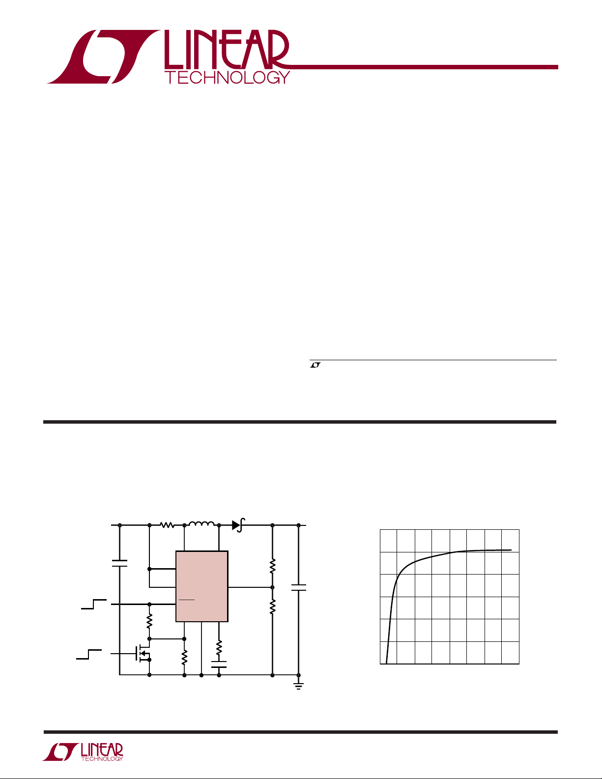
TYPICAL APPLICATIO
The LT®1618 step-up DC/DC converter combines a traditional voltage feedback loop and a unique current feedback
loop to operate as a constant-current, constant-voltage
source. This fixed frequency, current mode switcher operates from a wide input voltage range of 1.6V to 18V, and
the high switching frequency of 1.4MHz permits the use of
tiny, low profile inductors and capacitors. The current
sense voltage is set at 50mV and can be adjusted using the
I
pin.
ADJ
Available in the 10-Pin (3mm × 3mm) Exposed Pad DFN
and 10-pin MSOP packages, the LT1618 provides a complete solution for constant-current applications.
, LTC and LT are registered trademarks of Linear Technology Corporation.
(with Selectable 100mA/500mA Input Current Limit)
V
IN
5V
C1
4.7µF
3.3V
OFF
ON
0V
3.3V
100mA
500mA
0V
C1: TAIYO YUDEN JMK212BJ475
C2: TAIYO YUDEN EMK316BJ475
D1: ON SEMICONDUCTOR MBR0520
L1: SUMIDA CR43-100
USB to 12V Boost Converter
L1
3
8
9
13k
ISN
ISP
V
IN
SHDN
I
ADJ
10µH
2
LT1618
GND
SW
FB
V
C
5104
0.1Ω
20k
D1
7
R1
909k
1
R2
107k
2k
10nF
V
OUT
12V
C2
4.7µF
1618 TA01a
90
85
80
75
EFFICIENCY (%)
70
65
60
0
Efficiency Curve
20 60
40
LOAD CURRENT (mA)
100
120
160
1618 TA01b
sn1618 1618fas
80
140
1
LT1618
WW
W
ABSOLUTE AXI U RATI GS
U
(Note 1)
VIN, SHDN Voltage ................................................... 18V
SW Voltage .............................................................. 36V
ISP, ISN Voltage ...................................................... 36V
I
Voltage ............................................................... 6V
ADJ
FB Voltage .............................................................. 1.5V
Voltage .............................................................. 1.5V
V
C
UUW
PACKAGE/ORDER I FOR ATIO
TOP VIEW
10
FB
1
ISN
2
11
3
ISP
4
I
ADJ
5
GND
10-LEAD (3mm × 3mm) PLASTIC DFN
T
JMAX
DD PACKAGE
= 125°C, θJA = 43°C/W, θJC = 3°C/W
EXPOSED PAD (PIN 11) IS GND AND
MUST BE SOLDERED TO PCB
V
C
SHDN
9
V
8
IN
7
SW
6
SW
ORDER PART
NUMBER
LT1618EDD
DD PART
MARKING
LAFQ
Junction Temperature...........................................125°C
Operating Temperature Range (Note 2) .. – 40°C to 85°C
Storage Temperature Range
MSOP ............................................... – 65°C to 150°C
DFN ................................................. – 65°C to 125°C
Lead Temperature (Soldering, 10 sec) (MSOP) .... 300°C
ORDER PART
TOP VIEW
1
FB
2
ISN
3
ISP
4
I
ADJ
GND
5
MS PACKAGE
10-LEAD PLASTIC MSOP
T
= 125°C, θJA = 160°C/W
JMAX
10
V
C
9
SHDN
V
8
IN
SW
7
NC
6
NUMBER
LT1618EMS
MS PART
MARKING
LTNH
Consult LTC marketing for parts specified with wider operating temperature ranges.
ELECTRICAL CHARACTERISTICS
temperature range, otherwise specifications are at TA = 25°C. VIN = 1.6V, V
PARAMETER CONDITIONS MIN TYP MAX UNITS
Input Voltage 1.6 18 V
Quiescent Current V
Reference Voltage Measured at FB Pin 1.250 1.263 1.276 V
Reference Voltage Line Regulation 1.6V < VIN < 18V 0.01 0.03 %/V
FB Pin Bias Current VFB = 1.263V, VIN = 1.8V ● ±2 ±12 nA
Error Amplifier Voltage Gain 180 V/V
Error Amplifier Transconductance ∆IC = ± 5µA 160 µmho
Error Amplifier Sink Current VFB = 1.35V, VC = 1V 15 µA
Error Amplifier Source Current VFB = 1.10V, VC = 1V 30 µA
Current Sense Voltage (ISP, ISN) VFB = 0V, V
ISP, ISN Pin Bias Currents (Note 3) V
(ISP, ISN) Common Mode Minimum Voltage 1.8 V
Switching Frequency VFB = 1V 1.25 1.4 1.6 MHz
Maximum Switch Duty Cycle ● 88 92 %
Switch Current Limit (Note 4) 1.5 2.1 2.8 A
The ● denotes specifications which apply over the full operating
= 1.6V, unless otherwise noted.
SHDN
= 1.6V, Not Switching 1.8 2.7 mA
SHDN
= 0V 0.1 1 µA
V
SHDN
● 1.243 1.263 1.283 V
= 0V ● 47.5 50 52.5 mV
IADJ
= 1.85V, V
ISP
= 0V 550 kHz
V
FB
= 1.80V, V
ISN
= 0V 50 80 µA
IADJ
sn1618 1618fas
2
LT1618
TEMPERATURE (°C)
–50
PEAK CURRENT (A)
125
1618 G03
0
75
2.5
2.0
1.5
1.0
0.5
0
–25 25 50
100
ELECTRICAL CHARACTERISTICS
temperature range, otherwise specifications are at T
The ● denotes specifications which apply over the full operating
= 25°C. VIN = 1.6V, V
A
= 1.6V, unless otherwise noted.
SHDN
PARAMETER CONDITIONS MIN TYP MAX UNITS
Switch V
CESAT
ISW = 1A (Note 4) 200 260 mV
Switch Leakage Current Switch Off, VSW = 5V 0.01 5 µA
SHDN Pin Current V
= 1.6V 5 20 µA
SHDN
Shutdown Threshold (SHDN Pin) 0.3 V
Start-Up Threshold (SHDN Pin) 1V
Note 1: Absolute Maximum Ratings are those values beyond which the life
of a device may be impaired.
Note 2: The LT1618 is guaranteed to meet performance specifications
from 0°C to 70°C. Specifications over the –40°C to 85°C operating
temperature range are assured by design, characterization, and correlation
with statistical process controls.
Note 3: Bias currents flow into the ISP and ISN pins.
Note 4: Switch current limit and switch V
for the DD package is
CESAT
guaranteed by design and/or correlation to static test.
UW
TYPICAL PERFOR A CE CHARACTERISTICS
Switch Saturation Voltage
(V
500
CE, SAT
)
FB Pin Voltage and Bias Current
1.270
Switch Current Limit
4
400
TJ = 125°C
300
200
SATURATION VOLTAGE (mV)
100
0
TJ = 25°C
TJ = –50°C
0
0.5
1.0
SWITCH CURRENT (A)
Current Sense Voltage
(I
Pin = 0V)
ADJ
52
51
50
49
CURRENT SENSE VOLTAGE (mV)
1.5
1618 G01
1.265
1.260
FEEDBACK VOLTAGE (V)
1.255
1.250
2.0
CURRENT SENSE VOLTAGE (mV)
VOLTAGE
–25 25 50
–50
0
TEMPERATURE (°C)
Current Sense Voltage
(V
60
50
40
30
20
10
ISP, ISN
)
CURRENT
75
100
FB PIN BIAS CURRENT (nA)
2
0
–2
–4
125
1618 G02
Quiescent Current
2.5
2.0
1.5
1.0
QUIESCENT CURRENT (mA)
0.5
VIN = 18V
VIN = 1.6V
48
–25 25 50
–50
0
TEMPERATURE (°C)
75
100
1618 G04
125
0
0.0 0.2 0.4 0.6 0.8 1.0 1.2 1.4 1.6
I
PIN VOLTAGE (V)
ADJ
1618 G05
0
–25 25 50
–50
0
TEMPERATURE (°C)
75
100
1618 G06
sn1618 1618fas
125
3
LT1618
UW
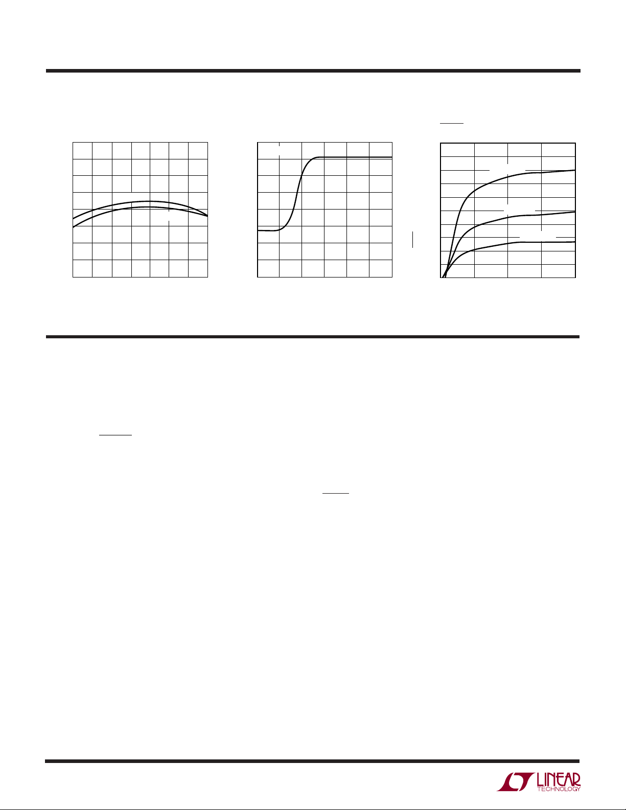
TYPICAL PERFOR A CE CHARACTERISTICS
Switching Frequency Frequency Foldback SHDN Pin Current
1.8
1.7
1.6
1.5
1.4
1.3
1.2
SWITCHING FREQUENCY (MHz)
1.1
1.0
–25 25 50
–50
VIN = 18V
0
TEMPERATURE (°C)
VIN = 1.6V
75
100
125
1618 G07
1.6
TJ = 25°C
1.4
1.2
1.0
0.8
0.6
0.4
SWITCHING FREQUENCY (MHz)
0.2
0
0 0.2
0.4 0.6
FEEDBACK PIN VOLTAGE (V)
0.8
1.0
1618 G08
1.2
50
45
40
35
30
25
20
15
SHDN PIN CURRENT (µA)
10
5
0
0
UUU
PIN FUNCTIONS
(MS/DD)
TJ = –50°C
TJ = 25°C
TJ = 125°C
5
SHUTDOWN PIN VOLTAGE (V)
10
15
20
1618 G09
FB (Pin 1/Pin 1): Feedback Pin. Set the output voltage by
selecting values for R1 and R2 (see Figure 1):
RR
⎛
12
⎜
⎝
V
OUT
.
1 263
⎞
–
1=
⎟
V
⎠
ISN (Pin 2/Pin 2): Current Sense (–) Pin. The inverting
input to the current sense amplifier.
ISP (Pin 3/Pin 3): Current Sense (+) Pin. The noninverting
input to the current sense amplifier.
I
(Pin 4/Pin 4): Current Sense Adjust Pin. A DC voltage
ADJ
applied to this pin will reduce the current sense voltage. If
this adjustment is not needed, tie this pin to ground.
GND (Pin 5/Pin 5): Ground Pin. Tie this pin directly to local
ground plane.
NC (Pin 6/NA): No Connection for MS Package.
SW (NA/Pin 6): Switch Pin for DD Package. Connect this
pin to Pin 7.
SW (Pin 7/Pin 7): Switch Pin. This is the collector of the
internal NPN power switch. Minimize the metal trace area
connected to this pin to minimize EMI.
VIN (Pin 8/Pin 8): Input Supply Pin. Bypass this pin with
a capacitor to ground as close to the device as possible.
SHDN (Pin 9/Pin 9): Shutdown Pin. Tie this pin higher
than 1V to turn on the LT1618; tie below 0.3V to turn it off.
VC (Pin 10/Pin 10): Compensation Pin for Error Amplifier.
Connect a series RC from this pin to ground. Typical values
are 2kΩ and 10nF.
Exposed Pad (NA/Pin 11): The Exposed Pad on the DD
package is GND and must be soldered to the PCB GND for
optimum thermal performance.
4
sn1618 1618fas
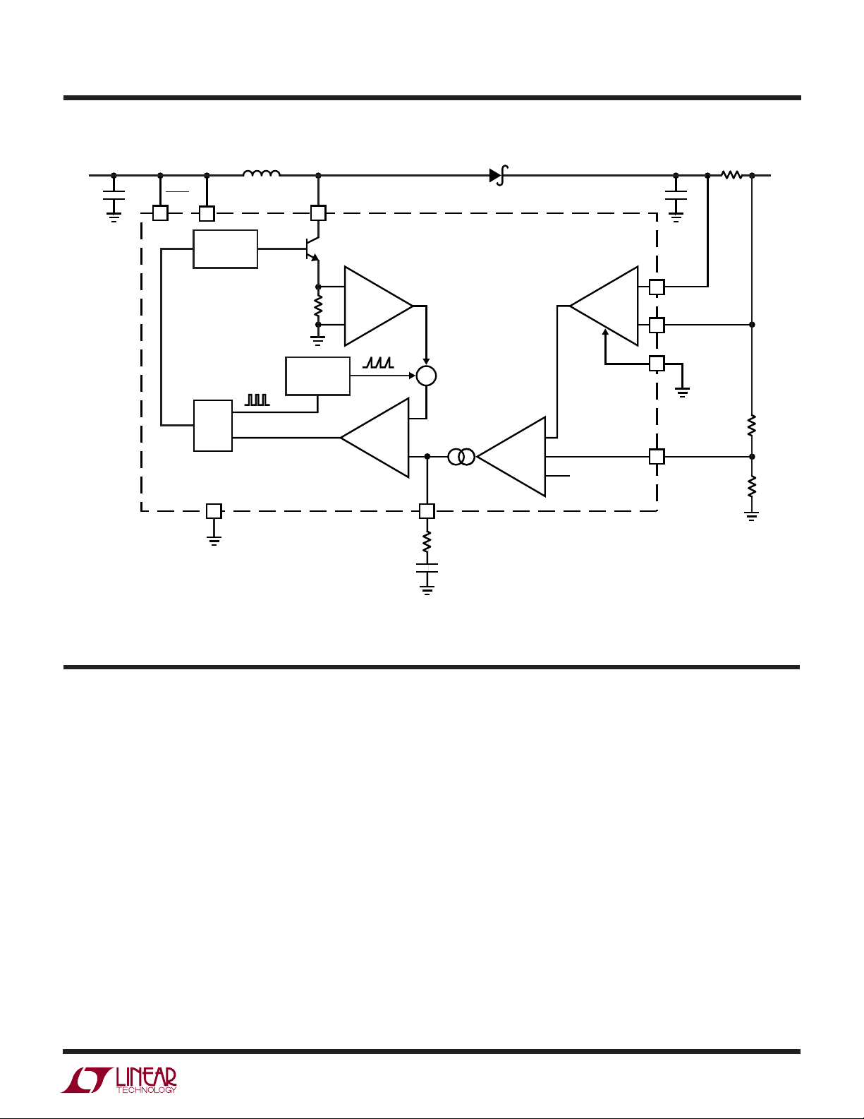
BLOCK DIAGRA
LT1618
W
V
IN
C1 C2
SHDN
V
8
DRIVER
L1
IN
SW
79
Q1
+
0.02Ω
×5
–
1.4MHz
OSCILLATOR
S
Q
R
A3
+
Σ
+
+
–
5 10
GND
V
C
R
C
C
D1
ISP
3
+
A1
×25
–
A2
–
1.263V
+
C
ISN
2
–
I
ADJ
4
FB
1
R
SENSE
V
OUT
R1
R2
Figure 1. LT1618 Block Diagram
U
OPERATIO
The LT1618 uses a constant frequency, current mode
control scheme to provide excellent line and load regulation. Operation can be best understood by referring to the
Block Diagram in Figure 1. At the start of each oscillator
cycle, the SR latch is set, turning on power switch Q1. The
signal at the noninverting input of PWM comparator A3 is
a scaled-down version of the switch current (summed
together with a portion of the oscillator ramp). When this
signal reaches the level set by the output of error amplifier
A2, comparator A3 resets the latch and turns off the power
switch. In this manner, A2 sets the correct peak current
level to keep the output in regulation. If the error amplifier’s
output increases, more current is delivered to the output;
if it decreases, less current is delivered. A2 has two
inverting inputs, one from the voltage feedback loop, and
one from the current feedback loop. Whichever inverting
input is higher takes precedence, forcing the converter
into either a constant-current or a constant-voltage mode.
The LT1618 is designed to transition cleanly between the
two modes of operation. Current sense amplifier A1 senses
the voltage between the ISP and ISN pins and provides a
25× level-shifted version to error amplifier A2. When the
voltage between ISP and ISN reaches 50mV, the output of
A1 provides 1.263V to one of the noninverting inputs of A2
and the converter is in constant-current mode. If the
current sense voltage exceeds 50mV, the output of A1 will
increase causing the output of A2 to decrease, thus
reducing the amount of current delivered to the output. In
this manner the current sense voltage is regulated to
50mV. Similarly, if the FB pin increases above 1.263V, the
output of A2 will decrease to reduce the peak current level
and regulate the output (constant-voltage mode).
sn1618 1618fas
5

LT1618
U
WUU
APPLICATIONS INFORMATION
Inductor Selection
Several inductors that work well with the LT1618 are listed
in Table 1, although there are many other manufacturers
and devices that can be used. Consult each manufacturer
for more detailed information and for their entire selection
of related parts. Many different sizes and shapes are
available. Ferrite core inductors should be used to obtain
the best efficiency, as core losses at 1.4MHz are much
lower for ferrite cores than for the cheaper powdered-iron
ones. Choose an inductor that can handle the necessary
peak current without saturating, and ensure that the
inductor has a low DCR (copper-wire resistance) to mini-
2
mize I
a good choice for many LT1618 designs.
Table 1. Recommended Inductors
PART (µH) (mΩ) (mm) VENDOR
CDRH5D18-4R1 4.1 57 2.0 Sumida
CDRH5D18-100 10 124 2.0 (847) 956-0666
CR43-2R2 2.2 71 3.5 www.sumida.com
CR43-4R7 4.7 109 3.5
CR43-100 10 182 3.5
CR54-100 10 100 4.8
LQH3C1R0M24 1.0 78 2.0 Murata
LQH3C2R2M24 2.2 126 2.0 (814) 237-1431
LQH3C4R7M24 4.7 260 2.0 www.murata.com
Capacitor Selection
Low ESR (equivalent series resistance) capacitors should
be used at the output to minimize the output ripple voltage.
Multilayer ceramic capacitors are an excellent choice.
They have an extremely low ESR and are available in very
small packages. X5R and X7R dielectrics are preferred, as
these materials retain their capacitance over wider voltage
and temperature ranges than other dielectrics. A 4.7µF to
10µF output capacitor is sufficient for high output current
designs. Converters with lower output currents may need
only a 1µF or 2.2µF output capacitor. Solid tantalum or
OSCON capacitors can be used, but they will occupy more
board area than a ceramic and will have a higher ESR for
R power losses. A 4.7µH or 10µH inductor will be
L MAX HEIGHT
the same footprint device. Always use a capacitor with a
sufficient voltage rating.
Ceramic capacitors also make a good choice for the input
decoupling capacitor, which should be placed as close as
possible to the VIN pin of the LT1618. A 1µF to 4.7µF input
capacitor is sufficient for most applications. Table 2 shows
a list of several ceramic capacitor manufacturers. Consult
the manufacturers for detailed information on their entire
selection of ceramic parts.
Table 2. Recommended Ceramic Capacitor Manufacturers
VENDOR PHONE URL
Taiyo Yuden (408) 573-4150 www.t-yuden.com
Murata (814) 237-1431 www.murata.com
Kemet (408) 986-0424 www.kemet.com
Diode Selection
Schottky diodes, with their low forward voltage drop and
fast switching speed, are the ideal choice for LT1618
applications. Table 3 shows several Schottky diodes that
work well with the LT1618. Many different manufacturers
make equivalent parts, but make sure that the component
chosen has a sufficient current rating and a voltage rating
greater than the output voltage. The diode conducts current only when the power switch is turned off (typically
less than half the time), so a 0.5A or 1A diode will be
sufficient for most designs. The companies below also
offer Schottky diodes with higher voltage and current
ratings.
Table 3. Recommended Schottky Diodes
1A PART 0.5A PART VENDOR PHONE/URL
UPS120 Microsemi (510) 353-0822
UPS130 www.microsemi.com
UPS140
MBRM120 MBR0520 ON Semiconductor (800) 282-9855
MBRM130 MBR0530 www.onsemi.com
MBRM140 MBR0540
B120 B0520 Diodes, Inc (805) 446-4800
B130 B0530 www.diodes.com
B140 B0540
6
sn1618 1618fas

LT1618
U
WUU
APPLICATIONS INFORMATION
Setting Output Voltage
To set the output voltage, select the values of R1 and R2
(see Figure 1) according to the following equation.
⎛
V
RR
12
OUT
⎜
.
1 263
⎝
For current source applications, use the FB pin for overvoltage protection. Pick R1 and R2 so that the output
voltage will not go too high if the load is disconnected or
if the load current drops below the preset value. Typically
choose R1 and R2 so that the overvoltage value will be
about 20% to 30% higher than the normal output voltage
(when in constant-current mode). This prevents the voltage loop from interfering with the current loop in current
source applications. For battery charger applications, pick
the values of R1 and R2 to give the desired end of charge
voltage.
⎞
–
1=
⎟
⎠
the output of the error amplifier (the VC pin) will be pulled
down and the LT1618 will stop switching.
A pulse width modulated (PWM) signal can also be used
to adjust the current sense voltage; simply add an RC
filterto convert the PWM signal into a DC voltage for the
I
pin. If the I
ADJ
pin is not used, it should be tied to
ADJ
ground. Do not leave the pin floating.
For applications needing only a simple one-step current
sense adjustment, the circuit in Figure 2 works well. If a
large value resistor (≥2MΩ) is placed between the I
ADJ
pin
and ground, the current sense voltage will reduce to about
25mV, providing a 50% reduction in current. Do not leave
the I
pin open. This method gives a well-regulated
ADJ
current value in both states, and is controlled by a logic
signal without the need for a variable PWM or DC control
signal. When the NMOS transistor is on, the current sense
voltage will be 50mV, when it is off, the current sense
voltage will be reduced to 25mV.
Selecting R
/Current Sense Adjustment
SENSE
Use the following formula to choose the correct current
sense resistor value (for constant current operation).
R
For designs needing an adjustable current level, the I
pin is provided. With the I
SENSE
= 50mV/I
MAX
pin tied to ground, the
ADJ
ADJ
nominal current sense voltage is 50mV (appearing between the ISP and ISN pins). Applying a positive DC
voltage to the I
pin will decrease the current sense
ADJ
voltage according to the following formula:
VV
1 263 0 8
V
ISENSE
.–(.)
=
25
For example, if 1V is applied to the I
IADJ
pin, the current
ADJ
sense voltage will be reduced to about 18mV. This
adjustability allows the regulated current to be reduced
without changing the current sense resistor (e.g. to adjust
brightness in an LED driver or to reduce the charge current
in a battery charger). If the I
pin is taken above 1.6V,
ADJ
LT1618
I
ADJ
FULL
CURRENT
2M
1618 F02
Figure 2
Considerations When Sensing Input Current
In addition to regulating the DC output current for currentsource applications, the constant-current loop of the
LT1618 can also be used to provide an accurate input
current limit. Boost converters cannot provide output
short-circuit protection, but the surge turn-on current can
be drastically reduced using the LT1618’s current sense
at the input. SEPICs, however, have an output that is DCisolated from the input, so an input current limit not only
helps soft-start the output but also provides excellent
short-circuit protection.
sn1618 1618fas
7

LT1618
U
WUU
APPLICATIONS INFORMATION
When sensing input current, the sense resistor should be
placed in front of the inductor (between the decoupling
capacitor and the inductor) as shown in the circuits in the
Typical Applications section. This will regulate the average
inductor current and maintain a consistent inductor ripple
current, which will, in turn, maintain a well regulated input
current. Do not place the sense resistor between the input
source and the input decoupling capacitor, as this may
allow the inductor ripple current to vary widely (even
though the average input current and the average inductor
current will still be regulated). Since the inductor current
is a triangular waveform (not a DC waveform like the
output current) some tweaking of the compensation
values (RC and CC on the VC pin) may be required to ensure
a clean inductor ripple current while the constant-current
loop is in effect. For these applications, the constantcurrent loop response can usually be improved by reducing the RC value, or by adding a capacitor (with a value of
approximately CC/10) in parallel with the RC and C
compensation network.
Frequency Compensation
The LT1618 has an external compensation pin (VC), which
allows the loop response to be optimized for each application. An external resistor and capacitor (or sometimes just
a capacitor) are placed at the VC pin to provide a pole and
a zero (or just a pole) to ensure proper loop compensation.
Numerous other poles and zeroes are present in the closed
C
loop transfer function of a switching regulator, so the V
C
pin pole and zero are positioned to provide the best loop
response. A thorough analysis of the switching regulator
control loop is not within the scope of this data sheet, and
will not be presented here, but values of 2kΩ and 10nF will
be a good choice for many designs. For those wishing to
optimize the compensation, use the 2kΩ and 10nF as a
starting point. For LED backlight applications where a
pulse-width modulation (PWM) signal is used to drive
the I
pin, the resistor is usually not included in the
ADJ
compensation network. This helps to provide additional
filtering of the PWM signal at the output of the error
amplifier (the VC pin).
Switch Node Considerations
To maximize efficiency, switch rise and fall times are made
as short as possible. To prevent radiation and high frequency resonance problems, proper layout of the high
frequency switching path is essential. Keep the output
switch (SW pin), diode and output capacitor as close
together as possible. Minimize the length and area of all
traces connected to the switch pin, and always use a
ground plane under the switching regulator to minimize
interplane coupling. The high speed switching current
path is shown in Figure 3. The signal path including the
switch, output diode and output capacitor contains nanosecond rise and fall times and should be kept as short as
possible.
8
SWITCH
L1
NODE
V
IN
HIGH
FREQUENCY
CIRCULATING
PATH
Figure 3
LOAD
V
1618 • F03
OUT
sn1618 1618fas

U
TYPICAL APPLICATIO S
4.5W Direct Broadcast Satellite (DBS) Power Supply with Short-Circuit Protection
LT1618
L1
V
IN
12V
4.7µF
C1
0.068Ω
C1: TAIYO YUDEN EMK316BJ475 (408) 573-4150
C2: TAIYO YUDEN TMK316BJ105 (408) 573-4150
C3, C4: TAIYO YUDEN TMK325BJ335 (408) 573-4150
D1: ON SEMICONDUCTOR MBRM140 (800) 282-9855
L1, L2: SUMIDA CR54-330 (847) 956-0666
L3: SUMIDA CR43-2R2 (847) 956-0666
33µH
2
ISN
3
ISP
LT1618
8
V
IN
9
SHDN
I
ADJ
GND
7
SW
FB
V
C
5104
R
C
2k
C
33nF
C2
1µF
1
C
80
D1
L2
33µH
RHCP
0V
ADD 5V
3.3V
LHCP
R5
24.9k
Efficiency
R1
100k
R2
10k
2.2µH
C3
3.3µF
L3
C4
3.3µF
MMBT3904
R3
10k
Q1
FMMT717
ZETEX
R4
1k
22kHz
NETWORK
TUNING
Q1
D2
MURS110
13.5V/18.5V
1618 TA02a
75
70
EFFICIENCY (%)
65
60
0
50 100 150 200
LOAD CURRENT (mA)
250 300
1618 TA02b
sn1618 1618fas
9

LT1618
TYPICAL APPLICATIONS
U
2-Cell White LED Driver
L1
V
IN
1.6V TO 3V
C1
4.7µF
10kHz TO 50kHz
PWM
BRIGHTNESS
ADJUST
C1: TAIYO YUDEN JMK212BJ475 (408) 573-4150
C2: TAIYO YUDEN EMK316BJ105 (408) 573-4150
D1: ON SEMICONDUCTOR MBR0520 (800) 282-9855
L1: SUMIDA CLQ4D10-4R7 (847) 956-0666
R3
5.1k
0.1µF
C3
4.7µH
87
V
IN
9
SHDN
LT1618
4
I
ADJ
GND
510
C
C
0.1µF
2-Cell Luxeon LED Driver
L1
V
1.8V TO 3V
IN
C1
1µF
10µH
87
V
IN
9
SHDN
LT1618
4
I
ADJ
GND
510
100nF
SW
ISP
ISN
V
SW
ISP
ISN
V
D1
2.49Ω
3
2
1
FB
C
C2
1µF
D1
0.15Ω
3
2
1
FB
C
C2
1µF
20mA
R1
2M
R2
160k
350mA
332k
124k
1618 • TA03
D2
10
C1, C2: TAIYO YUDEN JMK107BJ105KA
D1: ON SEMICONDUCTOR MBR0520
D2: LUMILEDS LXHL-BW02
L1: SUMIDA CR43-100
1618 • TA12
sn1618 1618fas

U
TYPICAL APPLICATIONS
LT1618
Li Ion White LED Driver
2.7V TO 5V
10kHz TO 50kHz
BRIGHTNESS
V
IN
2.7V TO 5V
C1
4.7µF
10kHz TO 50kHz
PWM
BRIGHTNESS
ADJUST
L1
V
IN
C1
4.7µF
PWM
ADJUST
C1: TAIYO YUDEN JMK212BJ475 (408) 573-4150
C2: TAIYO YUDEN TMK316BJ105 (408) 573-4150
D1: ON SEMICONDUCTOR MBR0530 (800) 282-9855
L1: SUMIDA CLQ4D10-100 (847) 956-0666
R3
5.1k
C3
0.1µF
10µH
87
V
IN
9
SHDN
LT1618
4
I
ADJ
GND
510
0.1µF
D1
SW
3
ISP
2
ISN
1
FB
V
C
C
C
White LED Driver for 20 LEDs
L1
D1
0.619Ω
SW
3
ISP
2
ISN
1
FB
V
C
C2
1µF
C
C
R3
5.1k
0.1µF
10µH
87
V
IN
9
SHDN
LT1618
4
I
ADJ
GND
C3
510
0.1µF
2.49Ω
C2
1µF
80mA
R1
2M
R2
121k
20mA
R1
2M
R2
100k
1618 • TA04
51Ω 51Ω 51Ω 51Ω
C1: TAIYO YUDEN JMK212BJ475 (408) 573-4150
C2: TAIYO YUDEN TMK316BJ105 (408) 573-4150
D1: ON SEMICONDUCTOR MBR0530 (800) 282-9855
L1: SUMIDA CR43-100 (847) 956-0666
1618 • TA05
sn1618 1618fas
11

LT1618
TYPICAL APPLICATIONS
USB to 5V SEPIC Converter
3
ISN
ISP
V
IN
SHDN
I
ADJ
10µH
2
LT1618
GND
5104
L1
SW
FB
V
C
I
IN
V
IN
5V
C1
4.7µF
3.3V
OFF
ON
0V
3.3V
100mA
500mA
0V
C1: TAIYO YUDEN JMK212BJ475 (408) 573-4150
C2: TAIYO YUDEN JMK316BJ106 (408) 573-4150
C3: TAIYO YUDEN EMK212BJ474 (408) 573-4150
D1: ON SEMICONDUCTOR MBR0520 (800) 282-9855
L1: SUMIDA CR43-100 (847) 956-0666
0.1Ω
8
9
20k
13k
U
7
2k
C3
0.47µF
1
10nF
D1
L2
10µH
R1
316k
R2
107k
V
OUT
5V
C2
10µF
1618 • TA09a
80
75
70
EFFICIENCY (%)
65
60
50 150 200
0
Efficiency
100
LOAD CURRENT (mA)
250
300
350
1618 F09b
V
OUT
2V/DIV
50mA/DIV
USB SEPIC During Start-Up
I
IN
1ms/DIV
1618 TA10
50mA/DIV
USB SEPIC Start-Up with Output Shorted
V
OUT
2V/DIV
1ms/DIV
1618 TA11
12
sn1618 1618fas

TYPICAL APPLICATIO S
12V Boost Converter with 500mA Input Current Limit
ISN
ISP
V
IN
SHDN
I
ADJ
4
L1
10µH
2
LT1618
GND
510
I
L1
V
IN
1.8V TO 5V
C1
4.7µF
C1: TAIYO YUDEN JMK212BJ475 (408) 573-4150
C2: TAIYO YUDEN EMK316BJ475 (408) 573-4150
D1: ON SEMICONDUCTOR MBR0520 (800) 282-9855
L1: SUMIDA CR43-100 (847) 956-0666
0.1Ω
3
8
9
U
SW
V
LT1618
D1
7
R1
909k
1
FB
R2
C
2k
10nF
107k
V
OUT
12V
C2
4.7µF
1618 • TA06a
90
85
80
75
EFFICIENCY (%)
70
65
60
20 60 100 160
0
Efficiency
VIN = 5V
VIN = 3.3V
40 80
L0AD CURRENT (mA)
120 140
1618 TA06b
12V Boost Converter Start-Up with Input Current Limit
V
OUT
5V/DIV
200mA/DIV
(VIN = 1.8V, I
I
LI
LOAD
50µs/DIV
= 40mA)
1618 TA07
12V Boost Converter Start-Up without Input Current Limit
V
OUT
5V/DIV
200mA/DIV
(VIN = 1.8V, I
I
LI
50µs/DIV
LOAD
= 40mA)
1618 TA08
sn1618 1618fas
13

LT1618
PACKAGE DESCRIPTIO
U
DD Package
10-Lead Plastic DFN (3mm × 3mm)
(Reference LTC DWG # 05-08-1698)
0.675 ±0.05
3.50 ±0.05
1.65 ±0.05
(2 SIDES)2.15 ±0.05
PACKAGE
OUTLINE
0.25 ± 0.05
RECOMMENDED SOLDER PAD PITCH AND DIMENSIONS
PIN 1
TOP MARK
(SEE NOTE 6)
0.200 REF
NOTE:
1. DRAWING TO BE MADE A JEDEC PACKAGE OUTLINE M0-229 VARIATION OF (WEED-2).
CHECK THE LTC WEBSITE DATA SHEET FOR CURRENT STATUS OF VARIATION ASSIGNMENT
2. DRAWING NOT TO SCALE
3. ALL DIMENSIONS ARE IN MILLIMETERS
4. DIMENSIONS OF EXPOSED PAD ON BOTTOM OF PACKAGE DO NOT INCLUDE
MOLD FLASH. MOLD FLASH, IF PRESENT, SHALL NOT EXCEED 0.15mm ON ANY SIDE
5. EXPOSED PAD SHALL BE SOLDER PLATED
6. SHADED AREA IS ONLY A REFERENCE FOR PIN 1 LOCATION ON THE
TOP AND BOTTOM OF PACKAGE
2.38 ±0.05
(2 SIDES)
0.50
BSC
3.00 ±0.10
(4 SIDES)
0.75 ±0.05
0.00 – 0.05
1.65 ± 0.10
(2 SIDES)
R = 0.115
TYP
2.38 ±0.10
(2 SIDES)
BOTTOM VIEW—EXPOSED PAD
106
15
0.25 ± 0.05
0.50 BSC
0.38 ± 0.10
(DD10) DFN 1103
14
sn1618 1618fas

PACKAGE DESCRIPTIO
U
MS Package
10-Lead Plastic MSOP
(Reference LTC DWG # 05-08-1661)
0.889 ± 0.127
(.035 ± .005)
LT1618
5.23
(.206)
MIN
0.305 ± 0.038
(.0120 ± .0015)
TYP
RECOMMENDED SOLDER PAD LAYOUT
0.254
(.010)
GAUGE PLANE
0.18
(.007)
NOTE:
1. DIMENSIONS IN MILLIMETER/(INCH)
2. DRAWING NOT TO SCALE
3. DIMENSION DOES NOT INCLUDE MOLD FLASH, PROTRUSIONS OR GATE BURRS.
MOLD FLASH, PROTRUSIONS OR GATE BURRS SHALL NOT EXCEED 0.152mm (.006") PER SIDE
4. DIMENSION DOES NOT INCLUDE INTERLEAD FLASH OR PROTRUSIONS.
INTERLEAD FLASH OR PROTRUSIONS SHALL NOT EXCEED 0.152mm (.006") PER SIDE
5. LEAD COPLANARITY (BOTTOM OF LEADS AFTER FORMING) SHALL BE 0.102mm (.004") MAX
3.20 – 3.45
(.126 – .136)
DETAIL “A”
DETAIL “A”
0.50
(.0197)
BSC
° – 6° TYP
0
0.53 ± 0.152
(.021 ± .006)
SEATING
PLANE
3.00 ± 0.102
(.118 ± .004)
(NOTE 3)
4.90 ± 0.152
(.193 ± .006)
(.043)
0.17 – 0.27
(.007 – .011)
TYP
1.10
MAX
12
0.50
(.0197)
BSC
8910
3
7
6
45
0.497 ± 0.076
(.0196 ± .003)
REF
3.00 ± 0.102
(.118 ± .004)
(NOTE 4)
0.86
(.034)
REF
0.127 ± 0.076
(.005 ± .003)
MSOP (MS) 0603
Information furnished by Linear Technology Corporation is believed to be accurate and reliable.
However, no responsibility is assumed for its use. Linear Technology Corporation makes no representation that the interconnection of its circuits as described herein will not infringe on existing patent rights.
sn1618 1618fas
15

LT1618
SHDN
I
ADJ
V
C
V
IN
SW
ISN
ISP
FB
LT1618
V
IN
16V
C1
4.7µF
2.2nF
220pF
1618 TA14
D1
D2
700mA
L1
47µH
3
2
1
9
8
7
GND
5104
C1: TAIYO YUDEN TMK325BJ475MN
D1: PHILIPS PMEG2010
D2: LUMILEDS DS45
L1: TOKO D104C
10k
0.07Ω
TYPICAL APPLICATIONS
U
RELATED PARTS
PART NUMBER DESCRIPTION COMMENTS
LT1613 550mA (ISW), 1.4MHz, High Efficiency Step-Up DC/DC Converter VIN: 0.9V to 10V, V
LT1615/LT1615-1 300mA/80mA (ISW), Constant Off-Time, High Efficiency Step-Up VIN: 1.2V to 15V, V
LT1930/LT1930A 1A (ISW), 1.2MHz/2.2MHz, High Efficiency Step-Up VIN: 2.6V to 16V, V
LT1932 Constant Current, 1.2MHz, High Efficiency White LED VIN: 1V to 10V, V
LT1944/LT1944-1 Dual Output 350mA/100mA (ISW), Constant Off-Time, VIN: 1.2V to 15V, V
(Dual) High Efficiency Step-Up DC/DC Converter MS Package
LT1945 (Dual) Dual Output, Pos/Neg, 350mA (ISW), Constant Off-Time, VIN: 1.2V to 15V, V
LT1961 1.5A (ISW), 1.25MHz, High Efficiency Step-Up DC/DC Converter VIN: 3V to 25V, V
LTC3401/LTC3402 1A/2A (ISW), 3MHz, Synchronous Step-Up DC/DC Converter VIN: 0.5V to 5V, V
LT3461/LT3461A 0.3A (ISW), 1.3MHz/3MHz, High Efficiency Step-Up DC/DC VIN: 2.5V to 16V, V
LT3463/LT3463A 250mA (ISW), Boost/Inverter Dual, Micropower DC/DC Converter VIN: 2.4V to 15V, V
LT3464 0.08A (ISW), High Efficiency Step-Up DC/DC Converter with VIN: 2.3V to 10V, V
LT3465/LT3465A Constant Current, 1.2MHz/2.7MHz, High Efficiency White LED VIN: 2.7V to 16V, V
LT3467/LT3467A 1.1A (ISW), 1.3MHz/2.1MHz, High Efficiency Step-Up DC/DC VIN: 2.4V to 16V, V
ThinSOT is a trademark of Linear Technology Corporation.
16
Li-Ion Buck-Boost Mode Luxeon LED Driver
D2
350mA
D1
7
100k
1
C
10k
10nF
3.2V TO 5V
0.15Ω
V
IN
2
8
9
C1
4.7µF
C1: TAIYO YUDEN JMK212BJ475KG
C2: TAIYO YUDEN EMK316BJ475ML
D1: ON SEMICONDUCTOR MBRM120
D2: LUMILEDS DS25
L1: NEC PLC-07453R3
ISP
ISN
V
IN
SHDN
I
ADJ
3.3µH
3
LT1618
GND
L1
SW
FB
V
5104
C2
4.7µF
1618 TA13
Buck Mode Luxeon LED Driver
ThinSOT
TM
OUT(MAX)
Package
OUT(MAX)
= 34V, IQ = 3mA, ISD < 1µA,
= 34V, IQ = 20µA, ISD < 1µA,
DC/DC Converter ThinSOT Package
= 34V, IQ = 4.2mA/5.5mA,
DC/DC Converter I
< 1µA, ThinSOT Package
SD
OUT(MAX)
OUT(MAX)
= 34V, IQ = 1.2mA, ISD < 1µA,
Boost Regulator ThinSOT Package
= 34V, IQ = 20µA, ISD < 1µA,
OUT(MAX)
= ±34V, IQ = 20µA, ISD < 1µA,
OUT(MAX)
High Efficiency Step-Up DC/DC Converter MS Package
OUT(MAX)
= 35V, IQ = 0.9mA, ISD < 6µA,
MS8E Package
= 6V, IQ = 38µA, ISD < 1µA,
Linear Technology Corporation
1630 McCarthy Blvd., Milpitas, CA 95035-7417
(408) 432-1900 ● FAX: (408) 434-0507
Converter with Integrated Schottky SC70 and ThinSOT Packages
with Integrated Schottky Diodes DFN Package
Integrated Schottky, Output Disconnect ThinSOT Package
Boost Regulator with Integrated Schottky Diode ThinSOT Package
Converter with Integrated Soft-Start ThinSOT Package
●
www.linear.com
MS Package
OUT(MAX)
= 38V, IQ = 2.8mA, ISD < 1µA,
OUT(MAX)
= ±40V, IQ = 40µA, ISD < 1µA,
OUT(MAX)
= 34V, IQ = 25µA, ISD < 1µA,
OUT(MAX)
= 34V, IQ = 1.9mA, ISD < 1µA,
OUT(MAX)
= 40V, IQ = 1.2mA, ISD < 1µA,
OUT(MAX)
LT/TP 0504 1K REV A • PRINTED IN USA
© LINEAR TECHNOLOGY CORPORATION 2001
sn1618 1618fas
 Loading...