

Linear Technology LT1613 Datasheet
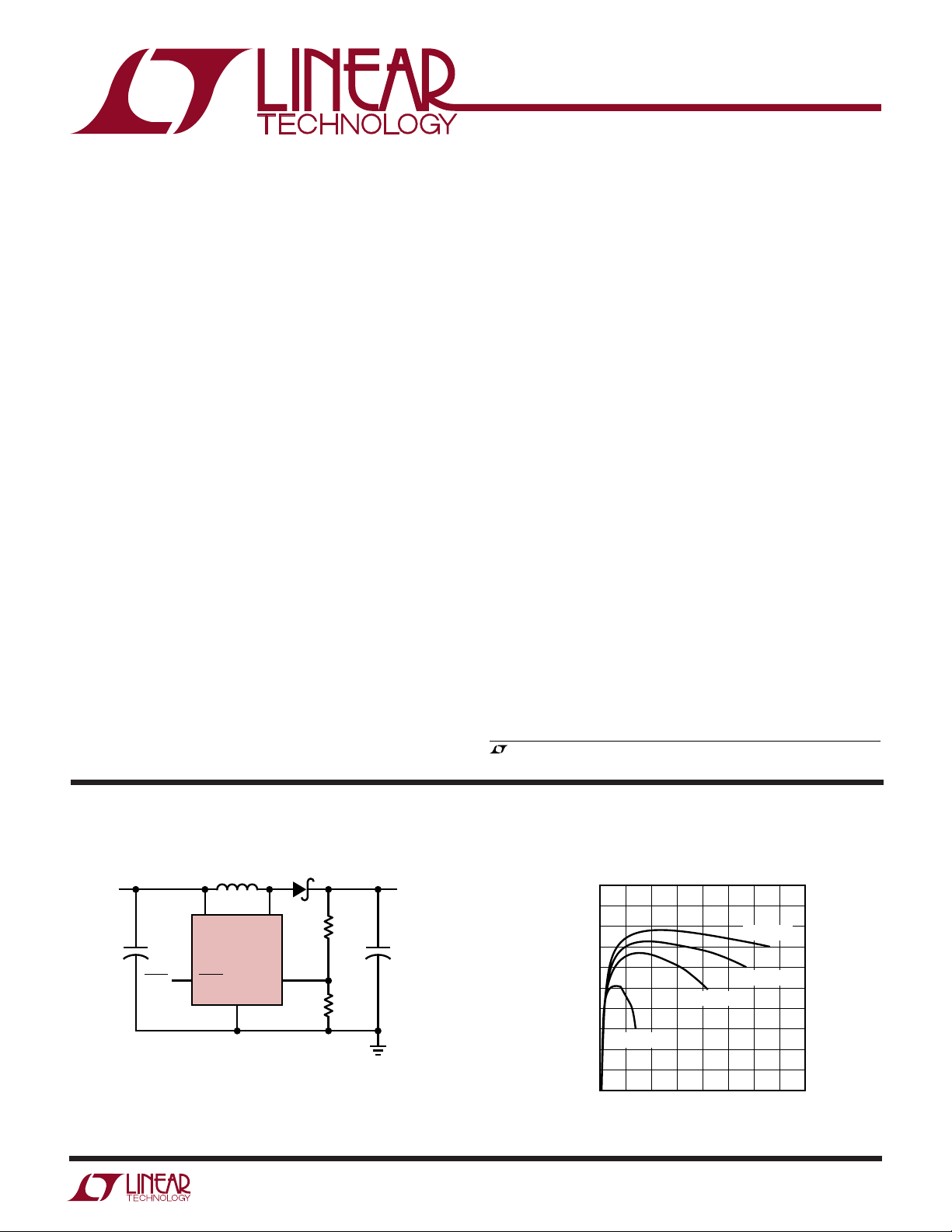
LOAD CURRENT (mA)
0 50 100 150 200 250 300 350 400
EFFICIENCY (%)
1613 TA01a
100
95
90
85
80
75
70
65
60
55
50
VIN = 4.2V
VIN = 3.5V
VIN = 2.8V
VIN = 1.5V
FEATURES
■
Uses Tiny Capacitors and Inductor
■
Internally Compensated
■
Fixed Frequency 1.4MHz Operation
■
Operates with VIN as Low as 1.1V
■
3V at 30mA from a Single Cell
■
5V at 200mA from 3.3V Input
■
15V at 60mA from Four Alkaline Cells
■
High Output Voltage: Up to 34V
■
Low Shutdown Current: <1µA
■
Low V
■
Tiny 5-Lead SOT-23 Package
Switch: 300mV at 300mA
CESAT
U
APPLICATIO S
■
Digital Cameras
■
Pagers
■
Cordless Phones
■
Battery Backup
■
LCD Bias
■
Medical Diagnostic Equipment
■
Local 5V or 12V Supply
■
External Modems
■
PC Cards
LT1613
1.4MHz, Single Cell DC/DC
Converter in 5-Lead SOT-23
U
DESCRIPTIO
The LT®1613 is the industry’s first 5-lead SOT-23 current
mode DC/DC converter. Intended for small, low power
applications, it operates from an input voltage as low as
1.1V and switches at 1.4MHz, allowing the use of tiny, low
cost capacitors and inductors 2mm or less in height. Its
small size and high switching frequency enables the
complete DC/DC converter function to take up less than
0.2 square inches of PC board area. Multiple output power
supplies can now use a separate regulator for each output
voltage, replacing cumbersome quasi-regulated approaches using a single regulator and a custom transformer.
A constant frequency, internally compensated current
mode PWM architecture results in low, predictable output
noise that is easy to filter. The high voltage switch on the
LT1613 is rated at 36V, making the device ideal for boost
converters up to 34V as well as for Single-Ended Primary
Inductance Converter (SEPIC) and flyback designs. The
device can generate 5V at up to 200mA from a 3.3V supply
or 5V at 175mA from four alkaline cells in a SEPIC design.
The LT1613 is available in the 5-lead SOT-23 package.
, LTC and LT are registered trademarks of Linear Technology Corporation.
TYPICAL APPLICATIO
V
IN
3.3V
+ +
C1
15µF
L1: MURATA LQH3C4R7M24 OR SUMIDA CD43-4R7
C1: AVX TAJA156M010
C2: AVX TAJB226M006
D1: MBR0520
Figure 1. 3.3V to 5V 200mA DC/DC Converter
4.7µH
V
IN
LT1613
SHDN
L1
GND
SW
U
D1
V
OUT
5V
R1
37.4k
FBSHDN
R2
12.1k
200mA
C2
22µF
1613 TA01
Efficiency Curve
1

LT1613
WW
W
ABSOLUTE MAXIMUM RA TIN GS
(Note 1)
VIN Voltage .............................................................. 10V
SW Voltage................................................–0.4V to 36V
FB Voltage ..................................................... VIN + 0.3V
Current into FB Pin ............................................... ±1mA
SHDN Voltage.......................................................... 10V
Maximum Junction Temperature..........................125°C
Operating Temperature Range
Commercial .............................................0°C to 70°C
U
U
W
PACKAGE/ORDER INFORMATION
ORDER PART NUMBER
TOP VIEW
SW 1
GND 2
FB 3
S5 PACKAGE
5-LEAD PLASTIC SOT-23
5 V
IN
4 SHDN
LT1613CS5
S5 PART MARKING
LTED
U
Extended Commercial (Note 2)........... –40°C to 85°C
Storage Temperature Range................. –65°C to 150°C
Lead Temperature (Soldering, 10 sec)..................300°C
Consult factory for Industrial and Military grade parts.
ELECTRICAL CHARACTERISTICS
temperature range, otherwise specifications are at TA = 25°C. Commercial grade 0°C to 70°C, VIN = 1.5V, V
otherwise noted. (Note 2)
PARAMETER CONDITIONS MIN TYP MAX UNITS
Minimum Operating Voltage 0.9 1.1 V
Maximum Operating Voltage 10 V
Feedback Voltage ● 1.205 1.23 1.255 V
FB Pin Bias Current ● 27 80 nA
Quiescent Current V
Quiescent Current in Shutdown V
Reference Line Regulation 1.5V ≤ VIN ≤ 10V 0.02 0.2 %/V
Switching Frequency ● 1.0 1.4 1.8 MHz
Maximum Duty Cycle ● 82 86 %
Switch Current Limit (Note 3) 550 800 mA
Switch V
CESAT
Switch Leakage Current VSW = 5V 0.01 1 µA
SHDN Input Voltage High 1V
SHDN Input Voltage Low 0.3 V
SHDN Pin Bias Current V
Note 1: Absolute Maximum Ratings are those values beyond which the life
of a device may be impaired.
= 1.5V 3 4.5 mA
SHDN
= 0V, VIN = 2V 0.01 0.5 µA
SHDN
= 0V, VIN = 5V 0.01 1.0 µA
V
SHDN
ISW = 300mA 300 350 mV
= 3V 25 50 µA
SHDN
V
= 0V 0.01 0.1 µA
SHDN
The ● denotes the specifications which apply over the full operating
= VIN unless
SHDN
Note 2: The LT1613C is guaranteed to meet performance specifications
from 0°C to 70°C. Specifications over the –40°C to 85°C operating
temperature range are assured by design, characterization and correlation
with statistical process controls.
Note 3: Current limit guaranteed by design and/or correlation to static test.
2
UW
TEMPERATURE (°C)
–50
FEEDBACK PIN VOLTAGE (V)
1613 G05
1.25
1.24
1.23
1.22
1.21
1.20
VOLTAGE
–25 0 25 50 75 100
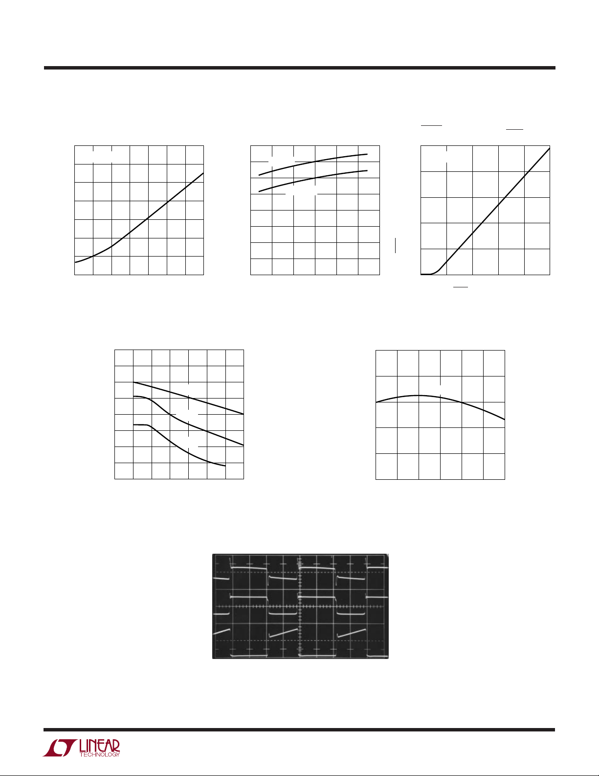
TYPICAL PERFOR A CE CHARACTERISTICS
Oscillator Frequency vs
Switch V
700
TA = 25°C
600
500
400
(mV)
300
CESAT
V
200
100
0
0 100 200 300 400 500 600 700
vs Switch Current SHDN Pin Current vs V
CESAT
SWITCH CURRENT (mA)
1613 G01
Temperature
2.00
1.75
1.50
1.25
1.00
0.75
0.50
SWITCHING FREQUENCY (MHz)
0.25
VIN = 5V
VIN = 1.5V
0
–50 –25 0 25 50 75 100
TEMPERATURE (°C)
1613 G02
LT1613
SHDN
50
TA = 25°C
40
30
20
10
SHDN PIN BIAS CURRENT (µA)
0
012345
SHDN PIN VOLTAGE (V)
1613 G03
Current Limit vs Duty Cycle
1000
900
800
700
600
500
CURRENT LIMIT (mA)
400
300
200
10 20 30 40 50 60 70 80
70°C
25°C
–40°C
DUTY CYCLE (%)
V
100mV/DIV
AC COUPLED
V
5V/DIV
Feedback Pin Voltage
1613 G04
Switching Waveforms, Circuit of Figure 1
OUT
SW
I
SW
200mA/DIV
= 150mA 200ns/DIV 1613 G06
I
LOAD
3
LT1613
UUU
PIN FUNCTIONS
SW (Pin 1): Switch Pin. Connect inductor/diode here.
Minimize trace area at this pin to keep EMI down.
GND (Pin 2): Ground. Tie directly to local ground plane.
FB (Pin 3): Feedback Pin. Reference voltage is 1.23V.
Connect resistive divider tap here. Minimize trace area at
FB. Set V
according to V
OUT
= 1.23V(1 + R1/R2).
OUT
W
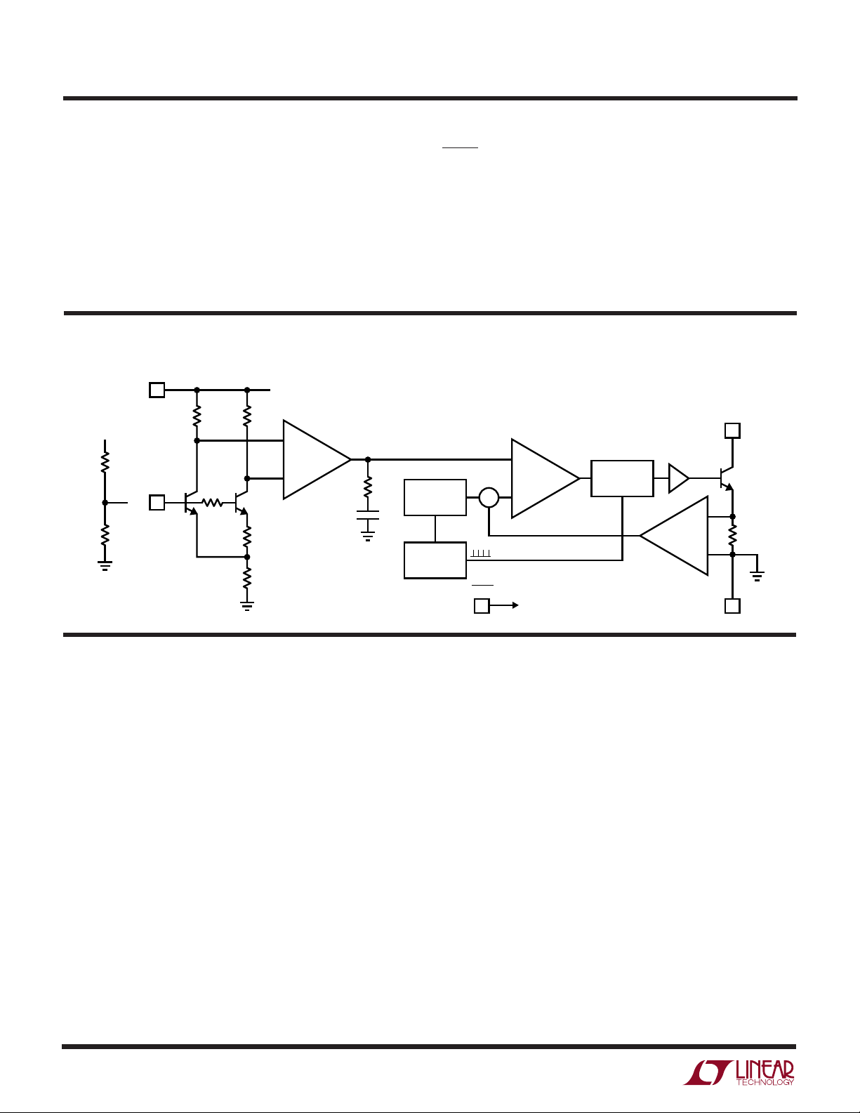
BLOCK DIAGRAM
Q2
x10
R6
40k
R3
30k
R4
140k
V
IN
+
A1
g
m
–
R
C
C
C
GENERATOR
1.4MHz
OSCILLATOR
V
OUT
R1
(EXTERNAL)
R2
(EXTERNAL)
V
5
IN
R5
40k
FB
Q1
3
FB
SHDN (Pin 4): Shutdown Pin. Tie to 1V or more to enable
device. Ground to shut down.
VIN (Pin 5): Input Supply Pin. Must be locally bypassed.
SW
1
Q3
+
0.15Ω
–
2
GND
1613 • BD
RAMP
SHDN
4
Σ
COMPARATOR
–
A2
+
SHUTDOWN
FF
RQ
S
DRIVER
U
OPERATIO
The LT1613 is a current mode, internally compensated,
fixed frequency step-up switching regulator. Operation
can be best understood by referring to the Block Diagram.
Q1 and Q2 form a bandgap reference core whose loop is
closed around the output of the regulator. The voltage
drop across R5 and R6 is low enough such that Q1 and Q2
do not saturate, even when VIN is 1V. When there is no
load, FB rises slightly above 1.23V, causing VC (the error
amplifier’s output) to decrease. Comparator A2’s output
stays high, keeping switch Q3 in the off state. As increased
output loading causes the FB voltage to decrease, A1’s
output increases. Switch current is regulated directly on a
cycle-by-cycle basis by the VC node. The flip flop is set at
the beginning of each switch cycle, turning on the switch.
When the summation of a signal representing switch
current and a ramp generator (introduced to avoid
subharmonic oscillations at duty factors greater than
50%) exceeds the VC signal, comparator A2 changes
state, resetting the flip flop and turning off the switch.
More power is delivered to the output as switch current is
increased. The output voltage, attenuated by external
resistor divider R1 and R2, appears at the FB pin, closing
the overall loop. Frequency compensation is provided
internally by RC and CC. Transient response can be optimized by the addition of a phase lead capacitor CPL in
parallel with R1 in applications where large value or low
ESR output capacitors are used.
As the load current is decreased, the switch turns on for a
shorter period each cycle. If the load current is further
decreased, the converter will skip cycles to maintain
output voltage regulation. If the FB pin voltage is increased
significantly above 1.23V, the LT1613 will enter a low
power state where quiescent current falls to approximately 100µA.
4
 Loading...