

FEATURES
LT1612
Synchronous, Step-Down
800kHz PWM
DC/DC Converter
U
DESCRIPTIO
■
Operates from Input Voltage As Low As 2V
■
Internal 0.7A Synchronous Switches
■
Uses Ceramic Input and Output Capacitors
■
620mV Reference Voltage
■
800kHz Fixed Frequency Switching
■
Programmable Burst Mode Operation
■
Low Quiescent Current: 160µA
■
8-Lead MSOP or SO Package
U
APPLICATIO S
■
Portable Devices
■
Lithium-Ion Step-Down Converters
■
5V to 3.3V Conversion
■
2-Cell Alkaline Step-Down Converters
U
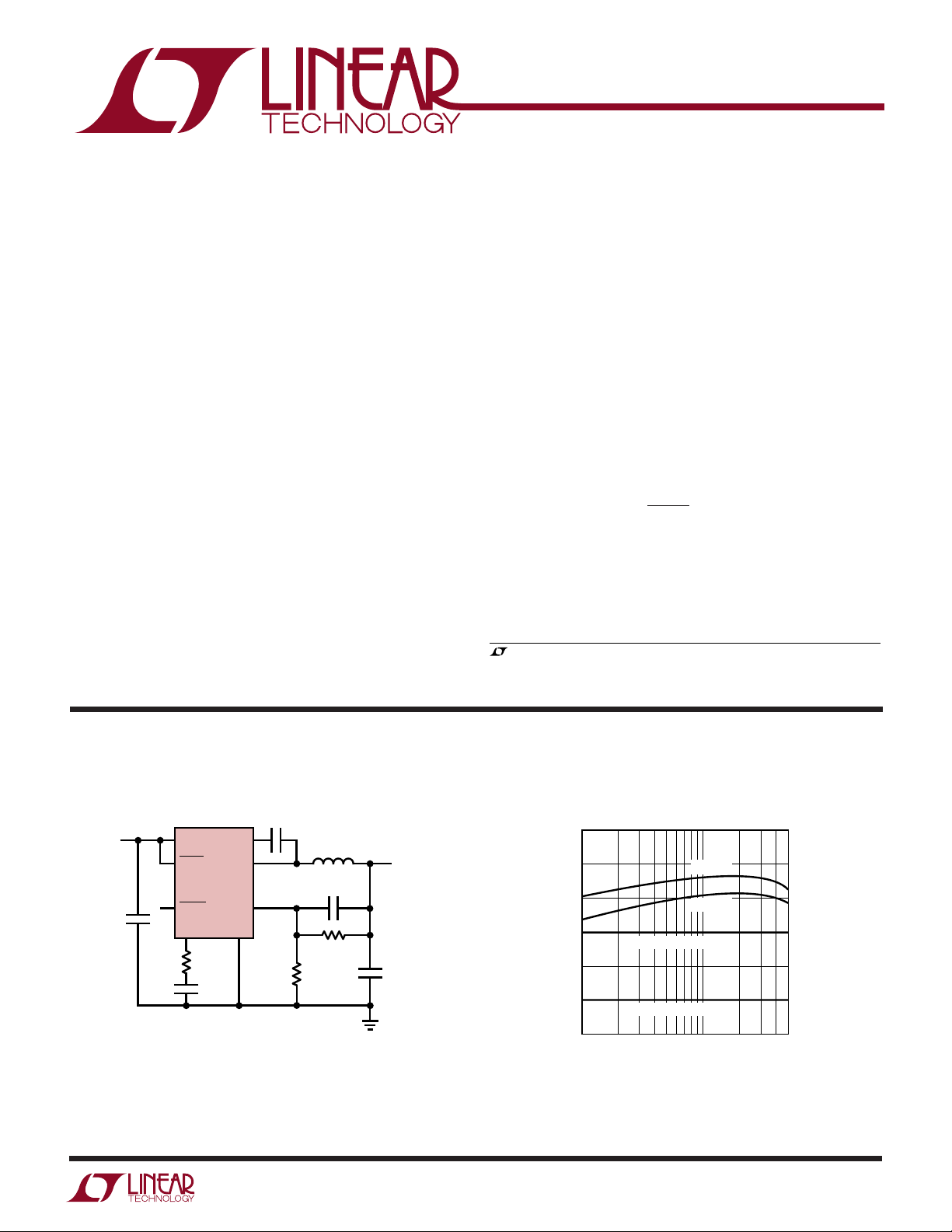
TYPICAL APPLICATION
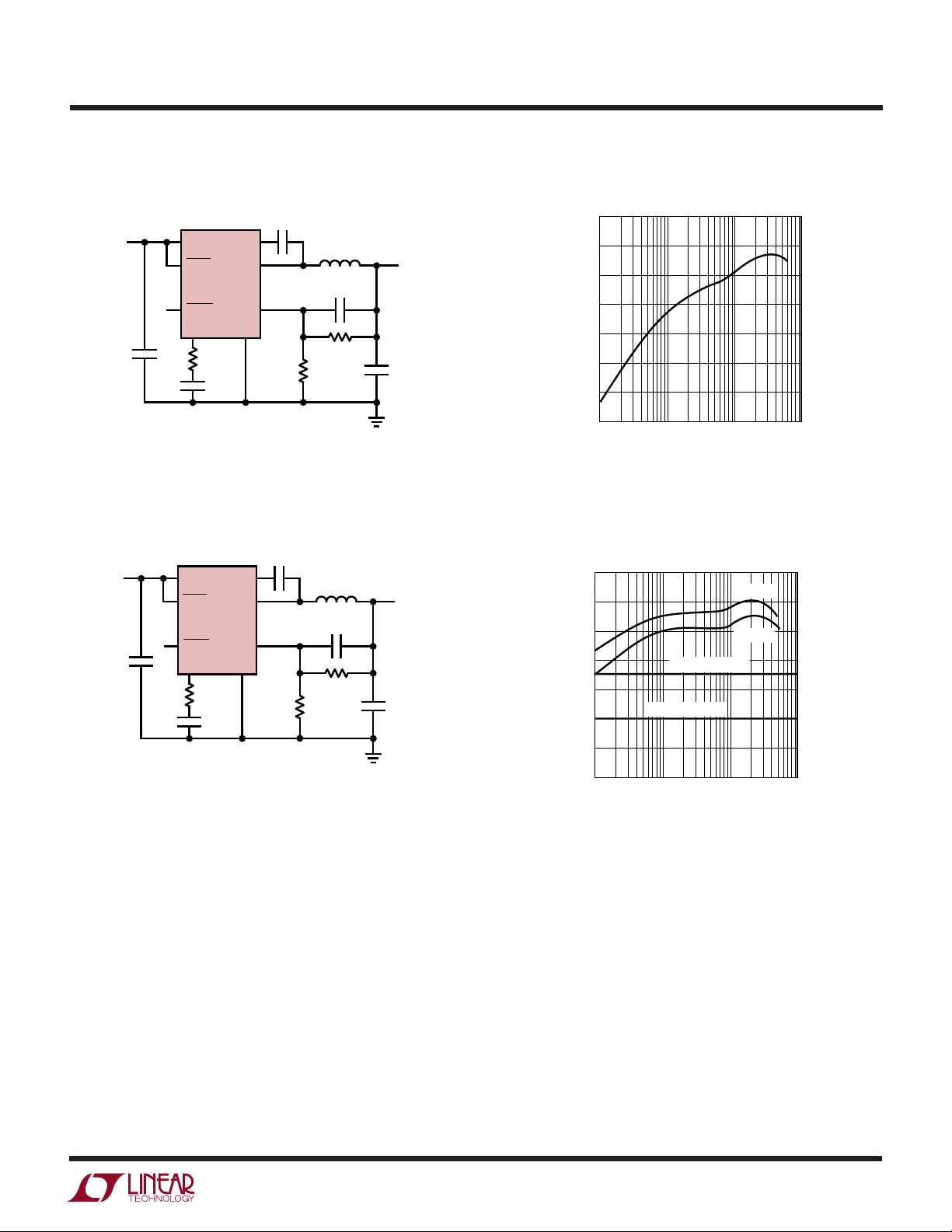
The LT®1612 is an 800kHz, synchronous step-down DC/
DC converter that operates from an input voltage as low
as 2V. Internal 0.45Ω switches deliver output currents up
to 500mA, and the 800kHz switching frequency allows the
use of small, low value ceramic input and output capacitors. Input voltage ranges from 5.5V down to 2V and
output voltage can be set as low as the 620mV reference.
The device features Burst ModeTM operation, keeping
efficiency high at light loads. Burst Mode operation can be
defeated by pulling the MODE pin high, enabling constant
switching throughout the load range for low noise.
No-load quiescent current is 160µA and shutdown current
is less than 1µA. The device is available in 8-lead SO and
MSOP packages.
, LTC and LT are registered trademarks of Linear Technology Corporation.
Burst Mode is a trademark of Linear Technology Corporation.
V
IN
2V
10µF
C1
V
IN
SHDN
LT1612
MODE
V
C
33.2k
330pF
C1: TAIYO-YUDEN JMK325BJ106MN
C2: PANASONIC EEFCDOF680R
L1: SUMIDA CD43-100
Figure 1. 2V to 1.2V Converter
BOOST
SW
GND
Efficiency for LT1612 vs Linear Regulator
V
= 1.2V
0.1µF
L1
10µH
100pF
FB
R1
215k
R2
232k
1%
1%
V
1.2V
500mA
C2
68µF
3.15V
OUT
1612 F01a
90
80
70
60
EFFICIENCY (%)
50
40
30
OUT
VIN = 2V
VIN = 3V
VIN = 2V (LINEAR)
VIN = 3V (LINEAR)
10010 500
LOAD CURRENT (mA)
1612 • F01b
sn1612 1612fs
1
LT1612
TOP VIEW
SHDN
MODE
BOOST
SW
V
C
FB
V
IN
GND
S8 PACKAGE
8-LEAD PLASTIC SO
1
2
3
4
8
7
6
5
WW
W
ABSOLUTE MAXIMUM RATINGS
U
(Note 1)
Supply Voltage (VIN)............................................... 5.5V
SW Pin Voltage....................................................... 5.5V
FB Pin Voltage ............................................... VIN + 0.3V
VC Pin Voltage ........................................................... 2V
SHDN Pin Voltage................................................... 5.5V
MODE Pin Voltage .................................................. 5.5V
U
W
PACKAGE/ORDER INFORMATION
ORDER PART
NUMBER
TOP VIEW
8
V
1
C
2
FB
3
V
IN
4
GND
MS8 PACKAGE
8-LEAD PLASTIC MSOP
T
= 125°C, θJA = 200°C/W
JMAX
7
6
5
SHDN
MODE
BOOST
SW
LT1612EMS8
MS8 PART MARKING
LTMS
BOOST Pin Voltage ....................................... VIN + 5.5V
Junction Temperature........................................... 125°C
Operating Temperature Range (Note 2) ... –40°C to 85°C
Storage Temperature Range ................. –65°C to 150°C
Lead Temperature (Soldering, 10 sec).................. 300°C
U
ORDER PART
NUMBER
LT1612ES8
S8 PART MARKING
T
= 125°C, θJA = 120°C/W
JMAX
1612
Consult factory for parts specified with wider operating temperature ranges.
ELECTRICAL CHARACTERISTICS
temperature range, otherwise specifications are TA = 25°C, V
SYMBOL PARAMETER CONDITIONS MIN TYP MAX UNITS
I
Q
V
FB
g
m
f
OSC
2
Quiescent Current MODE = 5V ● 12 mA
FB Voltage 0.605 0.62 0.635 V
FB Line Regulation ● 0.02 0.15 %/V
FB Pin Bias Current (Note 3) ● 750 nA
Error Amplifier Transconductance 250 µmhos
Min Input Voltage 2V
Max Input Voltage 5.5 V
Oscillator Frequency 700 800 900 kHz
f
Line Regulation 1%/V
OSC
Maximum Duty Cycle 85 90 %
Shutdown Threshold Minimum Voltage for Active
The ● denotes specifications which apply over the full operating
= V
IN
MODE = 0V, Not Switching
SHDN = 0V ● 1 µA
Maximum Voltage for Shutdown ● 0.2 V
SHDN
= 3V
● 160 220 µA
● 0.60 0.62 0.635 V
● 550 1100 kHz
● 80 %
● 2V
sn1612 1612fs
LT1612
ELECTRICAL CHARACTERISTICS
temperature range, otherwise specifications are TA = 25°C, V
The ● denotes specifications which apply over the full operating
IN
= V
SHDN
= 3V
SYMBOL PARAMETER CONDITIONS MIN TYP MAX UNITS
SHDN Pin Current SHDN = 2V
● 10 15 µA
SHDN = 5V ● 30 45 µA
BOOST Pin Current BOOST = VIN + 2V 4 mA
Switch Current Limit (Note 4) Duty Cycle = 0% MODE = OV 600 710 900 mA
MODE = 5V 550 650 900 mA
Burst Mode Operation Current Limit MODE = 0V 180 mA
Switch Voltage Drop ISW = 500mA 200 280 mV
Rectifier Voltage Drop I
SW Pin Leakage VSW = 5V, V
Note 1: Absolute Maximum Ratings are those values beyond which the life
of a device may be impaired.
Note 2: The LT1612E is guaranteed to meet performance specifications
from 0°C to 70°C. Specifications over the –40°C to 85°C operating
= 500mA 300 400 mV
RECT
= 0V ● 1 µA
SHDN
temperature range are assured by design, characterization and correlation
with statistical process controls.
Note 3: Bias current flows out of the FB pin.
Note 4: Duty cycle affects current limit due to slope compensation.
UW
TYPICAL PERFOR A CE CHARACTERISTICS
FB Voltage vs Temperature
0.64
0.63
0.62
0.61
FB VOLTAGE (V)
0.60
0.59
–50
02550
–25
TEMPERATURE (°C)
75 100
1612 • G01
Quiescent Current vs Temperature
190
MODE = 0V
180
170
160
150
140
130
120
QUIESCENT CURRENT (µA)
110
100
–50 –25 25 75
0 100
TEMPERATURE (°C)
50
1612 • G02
FB Pin Bias Current
0
–2
–4
–6
–8
–10
–12
–14
FB PIN CURRENT (nA)
–16
–18
–20
–50
–25
25
0
TEMPERATURE (°C)
50 75
100
1612 • G03
sn1612 1612fs
3
LT1612
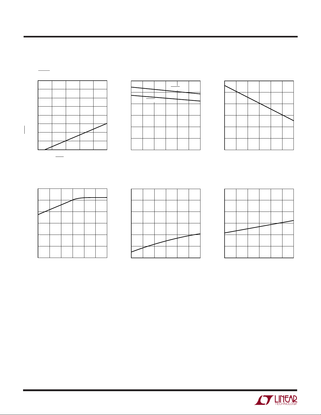
TEMPERATURE (°C)
–50
OSCILLATOR FREQUENCY (kHz)
1000
900
800
700
600
500
400
–25
02550
1612 • G06
75 100
RECTIFIER CURRENT (mA)
0
RECTIFIER VOLTAGE DROP (mV)
600
500
400
300
200
100
0
100
200 300 400
1612 • G09
500 600
UW
TYPICAL PERFOR A CE CHARACTERISTICS
SHDN Pin Bias Current
80
70
60
50
40
30
20
SHDN PIN CURRENT (µA)
10
0
12 4
0
SHDN PIN VOLTAGE (V)
Maximum Duty Cycle vs
Temperature
94
90
86
Switch Current Limit vs
Temperature
800
700
600
500
400
SWITCH CURRENT (mA)
300
3
5
1612 • G04
200
–50
MODE = 5V
02550
–25
TEMPERATURE (°C)
MODE = 0V
75 100
1612 • G05
Switch Voltage Drop
600
500
400
Oscillator Frequency vs
Temperature
Rectifier Voltage Drop
82
78
MAXIMUM DUTY CYCLE (%)
74
70
–50
02550
–25
TEMPERATURE (°C)
75 100
1612 • G07
300
200
SWITCH VOLTAGE DROP (mV)
100
0
0
200 300 400
100
SWITCH CURRENT (mA)
500 600
1612 • G08
4
sn1612 1612fs

UUU
PIN FUNCTIONS
LT1612
VC (Pin 1): Compensation Pin. This is the current sink/
source output of the error amplifier. By connecting an RC
network from this pin to ground, frequency response can
be tuned for a wide range of circuit configurations. The
voltage at this pin also sets the current limit, and if
grounded, the switch will remain in the OFF state.
FB (Pin 2): Feedback Pin. This pin is the negative input to
the error amplifier. Connect the resistor divider tap to this
point which sets V
V
= 0.62V (1 + R1/R2)
OUT
according to:
OUT
VIN (Pin 3): Supply Pin. Bypass capacitor C1 must be right
next to this pin.
GND (Pin 4): Ground Pin. Connect directly to local ground
plane.
W
BLOCK DIAGRA
SW (Pin 5): Switch Pin. Connect inductor and boost
capacitor here. Minimize trace area at this pin to keep EMI
down.
BOOST (Pin 6): This is the supply pin for the switch driver
and must be above VIN by 1.5V for proper switch operation. Connect the boost capacitor to this pin.
MODE (Pin 7): Burst Mode Operation Disable Pin. For
continuous switching operation (low noise), pull this pin
above 2V. For Burst Mode operation which gives better
light load efficiency, tie to ground. Output ripple voltage in
Burst Mode operation is typically 30mV
. See applica-
P-P
tions section for more information about this function.
SHDN (Pin 8): Shutdown Pin. Pull this pin low for shut-
down mode. Tie to a voltage between 2V and 5.5V for
normal operation.
MODE
SHDN
R
SENSE
V
3
IN
V
1
C
2
FB
7
8
–
+
0.62V
SHUTDOWN
A1
+
–
0.7V
A3
ENABLE
OSCILLATOR
V/I
0.08Ω
+
A2
–
FLIP-FLOP
RQ
SLOPE
COMPENSATION
S
SWITCH
DRIVER
RECTIFIER
DRIVE
BOOST DIODE
SWITCH
RECTIFIER
6
5
4
BOOST
SW
GND
1612 BD
sn1612 1612fs
5

LT1612
OPERATIO
U
The LT1612 employs fixed frequency, current mode control. This type of control uses two feedback loops. The
main control loop sets output voltage and operates as
follows: A load step causes V
and the FB voltage to be
OUT
perturbed slightly. The error amplifier responds to this
change in FB by driving the VC pin either higher or lower.
Because switch current is proportional to the VC pin
voltage, this change causes the switch current to be
adjusted until V
is once again satisfied. Loop compen-
OUT
sation is taken care of by an RC network from the VC pin
to ground.
Inside this main loop is another that sets current limit on
a cycle-by-cycle basis. This loop utilizes current comparator A2 to control peak current. The oscillator runs at
800kHz and issues a set pulse to the flip-flop at the
beginning of each cycle, turning the switch on. With the
switch now in the ON state the SW pin is effectively
connected to VIN. Current ramps up in the inductor linearly
at a rate of (VIN – V
pin voltage and when the voltage across R
)/L. Switch current is set by the V
OUT
trips the
SENSE
C
current comparator, a reset pulse will be generated and the
switch will be turned off. Since the inductor is now loaded
up with current, the SW pin will fly low and trigger the
rectifier to turn on. Current will flow through the rectifier
decreasing at a rate of V
/L until the oscillator issues a
OUT
new set pulse, causing the cycle to repeat.
If the load is light and VC decreases below A3’s trip point,
the device will enter the Burst Mode operation region (the
MODE pin must be at ground or floating). In this state the
oscillator and all other circuitry except the reference and
comparator A3 are switched on and off at low frequency.
This mode of operation increases efficiency at light loads
but introduces low frequency voltage ripple at the output.
For continuous switching and no low frequency output
voltage ripple, pull the MODE pin high. This will disable
comparator A3 which forces the oscillator to run
continuously.
Layout Hints
The LT1612 switches current at high speed, mandating
careful attention to layout for proper performance.
will not get advertised performance with careless layout
You
.
Figure 2 shows recommended component placement for
a buck (step-down) converter. Follow this closely in your
PC layout. Note the direct path of the switching loops.
Input capacitor C1 must be placed close (< 5mm) to the IC
package. As little as 10mm of wire or PC trace from CIN to
VIN will cause problems such as inability to regulate or
oscillation.
The ground terminal of input capacitor C1 should tie close
to Pin 4 of the LT1612. Doing this reduces dI/dt in the
ground copper which keeps high frequency spikes to a
minimum. The DC/DC converter ground should tie to the
PC board ground plane at one place only, to avoid introducing dI/dt in the ground plane.
C
R1
R2 R
V
IN
MULTIPLE
VIAs
Figure 2. Recommended Component Placement. Traces
Carrying High Current are Direct. Trace Area at FB Pin and V
Pin Is Kept Low. Lead Length to Battery Should Be Kept Short
C
C
SHDN
8
MODE
7
6
5
C3
L1
1612 F02
V
OUT
C
C1
GND
1
2
LT1612
3
4
C2
6
sn1612 1612fs

OPERATIO
LT1612
U
Burst Mode Operation Defeat
To maintain high efficiency at light loads, the LT1612 will
automatically shift into Burst Mode operation (MODE = 0V
or floating). In this mode of operation the oscillator and
switch drive circuitry is alternately turned on and off,
reducing quiescent current to 160µA. This reduces power
V
OUT
20mV/DIV
AC COUPLED
IL
200mA/DIV
P-P
1612 F03
for
5µs/DIV
Figure 3. Output Voltage Ripple is 20mV
the Circuit of Figure 1
consumption but also adds low frequency voltage ripple to
the output. Figure 3 shows switching waveforms for a 5V
to 3.3V converter running in Burst Mode operation. Output
voltage ripple is approximately 20mV
. If the MODE pin
P-P
is pulled high, Burst Mode operation will be inhibited and
the oscillator runs continuously with no low frequency
ripple at the output. See Figures 4 and 5.
V
OUT
200mV/DIV
AC COUPLED
I
L
200mA/DIV
I
10mA TO 310mA
LOAD
0.1ms/DIV
1612 F04
Figure 4. Transient Response for the Circuit of Figure 1
with the MODE Pin Tied to Ground or Floating
V
OUT
200mV/DIV
AC COUPLED
I
L
200mA/DIV
I
10mA TO 300mA
LOAD
0.1ms/DIV
Figure 5. With the MODE Pin Tied High, Low
Frequency Output Voltage Ripple Is No Longer Present
1612 F05
sn1612 1612fs
7

LT1612
U
TYPICAL APPLICATIONS
V
2.7V TO 4.2V
10µF
CERAMIC
V
50mV/DIV
OUT
Single Li-Ion to 2V Converter
IN
C1: TAIYO-YUDEN LMK325BJ106MN
C2: TAIYO-YUDEN LMK325BJ226MN
L1: SUMIDA CD43-100
V
IN
SHDN
MODE
V
C
30.1k
BOOST
LT1612
GND
680pF
Transient Response
SW
Li-Ion to 2V Converter Efficiency
0.1µF
L1
10µH
20pF
FB
1M
453k
1%
1%
V
OUT
2V
500mA
22µF
CERAMIC
1612 TA02
85
80
VIN = 2.8V
75
70
65
EFFICIENCY (%)
60
55
50
1
VIN = 4.2V
VIN = 3.5V
10 100 1000
LOAD CURRENT (mA)
1612 TA04
Burst Mode Operation
V
20mV/DIV
OUT
I
200mA/DIV
L
LOAD STEP
125mA TO 300mA
VIN = 4V
V
= 2V
OUT
MODE = HIGH
100µs/DIV
V
V
2V/DIV
OUT
INRUSH
CURRENT
200mA/DIV
5V/DIV
SHDN
100mA/DIV
I
L
1612 TA03
Inrush Current at Start-Up
0.2ms/DIV
MODE = LOW
1612 TA06
5µs/DIV
1612 TA05
8
sn1612 1612fs
U
TYPICAL APPLICATIONS
LT1612
V
IN
5V
10µF
CERAMIC
V
IN
2V
C1
10µF
5V to 2.5V Converter
BOOST
V
IN
C
30.1k
SW
LT1612
FB
GND
680pF
SHDN
MODE
V
C1
C1: TAIYO-YUDEN LMK325BJ106MN
C2: TAIYO-YUDEN LMK325BJ226MN
L1: SUMIDA CD43-100
2V to 0.9V Converter Efficiency for LT1612 vs Linear Regulator.
BOOST
V
IN
LT1612
C
33.2k
SW
FB
GND
330pF
SHDN
MODE
V
C1: TAIYO-YUDEN JMK325BJ106MN
C2: PANASONIC EEFCDOF680R
L1: SUMIDA CD43-100
0.1µF
0.1µF
232k
5V to 2.5V Converter Efficiency
85
L1
10µH
20pF
1M
332k
L1
10µH
100pF
R1
105k
R2
V
OUT
2.5V
500mA
C2
22µF
CERAMIC
1612 TA07
V
OUT
0.9V
500mA
C2
68µF
3.15V
1612 TA09
80
75
70
65
EFFICIENCY (%)
60
55
50
1
80
70
60
50
40
EFFICIENCY (%)
30
20
10
1
10 100 1000
LOAD CURRENT (mA)
1612 TA08
V
= 0.9V.
OUT
VIN = 2V
VIN = 3V
V
= 2V (LINEAR)
IN
VIN = 3V (LINEAR)
10 100 1000
LOAD CURRENT (mA)
1612 TA10
sn1612 1612fs
9

LT1612
PACKAGE DESCRIPTION
U
Dimension in inches (millimeters) unless otherwise noted.
MS8 Package
8-Lead Plastic MSOP
(LTC DWG # 05-08-1660)
0.118 ± 0.004*
(3.00 ± 0.102)
8
7
6
5
0.193 ± 0.006
(4.90 ± 0.15)
12
0.043
(1.10)
MAX
0.007
(0.18)
0.021
± 0.006
(0.53 ± 0.015)
* DIMENSION DOES NOT INCLUDE MOLD FLASH, PROTRUSIONS OR GATE BURRS. MOLD FLASH,
PROTRUSIONS OR GATE BURRS SHALL NOT EXCEED 0.006" (0.152mm) PER SIDE
** DIMENSION DOES NOT INCLUDE INTERLEAD FLASH OR PROTRUSIONS.
INTERLEAD FLASH OR PROTRUSIONS SHALL NOT EXCEED 0.006" (0.152mm) PER SIDE
° – 6° TYP
0
SEATING
PLANE
0.009 – 0.015
(0.22 – 0.38)
0.0256
(0.65)
BSC
4
3
0.118 ± 0.004**
(3.00 ± 0.102)
0.034
(0.86)
REF
0.005
± 0.002
(0.13 ± 0.05)
MSOP (MS8) 1100
10
sn1612 1612fs

PACKAGE DESCRIPTION
U
Dimension in inches (millimeters) unless otherwise noted.
S8 Package
8-Lead Plastic Small Outline (Narrow 0.150)
(LTC DWG # 05-08-1610)
0.189 – 0.197*
(4.801 – 5.004)
7
8
5
6
LT1612
0.228 – 0.244
(5.791 – 6.197)
0.010 – 0.020
(0.254 – 0.508)
0.008 – 0.010
(0.203 – 0.254)
*
DIMENSION DOES NOT INCLUDE MOLD FLASH. MOLD FLASH
SHALL NOT EXCEED 0.006" (0.152mm) PER SIDE
**
DIMENSION DOES NOT INCLUDE INTERLEAD FLASH. INTERLEAD
FLASH SHALL NOT EXCEED 0.010" (0.254mm) PER SIDE
×
°
45
0.016 – 0.050
(0.406 – 1.270)
0°– 8° TYP
0.053 – 0.069
(1.346 – 1.752)
0.014 – 0.019
(0.355 – 0.483)
TYP
0.150 – 0.157**
(3.810 – 3.988)
SO8 1298
1
3
2
4
0.004 – 0.010
(0.101 – 0.254)
0.050
(1.270)
BSC
Information furnished by Linear Technology Corporation is believed to be accurate and reliable.
However, no responsibility is assumed for its use. Linear Technology Corporation makes no representation that the interconnection of its circuits as described herein will not infringe on existing patent rights.
sn1612 1612fs
11

LT1612
TYPICAL APPLICATIO
U
5V to 3.3V Converter
V
IN
5V
10µF
C1
V
IN
SHDN
LT1612
MODE
V
C
R3
33.2k
C4
680pF
C1: TAIYO-YUDEN LMK325BJ106MN
C2: TAIYO-YUDEN LMK325BJ226MN
L1: SUMIDA CD43-100
BOOST
SW
GND
C3
0.1µF
L1
10µH
20pF
FB
R2
232k
1%
R1
1M
1%
C2
22µF
V
OUT
3.3V
500mA
1612 TA01a
85
VIN = 5V
V
OUT
80
75
70
65
EFFICIENCY (%)
60
55
50
1
Efficiency
= 3.3V
10 100 1000
LOAD CURRENT (mA)
1612 TA01b
RELATED PARTS
PART NUMBER DESCRIPTION COMMENTS
LTC®1474 Low IQ Step-Down Switching Regulator 10µA IQ, VIN from 3V to 18V, MSOP Package up to 300mA
LT1616 600mA, 1.4MHz Step-Down Regulator in SOT-23 VIN from 3.6V to 25V, SOT-23 Package
LTC1701 SOT-23 Step-Down Switching Regulator 500mA in SOT-23 Package, 1MHz Switching Frequency
LTC1707 Monolithic Synchronous Step-Down Switching Regulator 500mA, VIN from 2.65V to 8.5V
LTC1772 Constant Frequency Step-Down Controller in SOT-23 High Current, High Efficiency: Up to 94%
LTC1877/LTC1878 High Efficiency, Monolithic Synchronous Step-Down Regulator 10µA IQ, 2.65≤ VIN ≤ 10V, MSOP Package up to 600mA
LTC3404 1.4MHz High Efficiency Monolithic Synchronous Step-Down Reg 10µA IQ, High Efficiency: up to 95%, MSOP Package
12
Linear Technology Corporation
1630 McCarthy Blvd., Milpitas, CA 95035-7417
(408) 432-1900 ● FAX: (408) 434-0507
●
www.linear-tech.com
sn1612 1612fs
LT/TP 1100 4K • PRINTED IN USA
LINEAR TECHNOLOGY CORPORATION 1999
 Loading...