

Linear Technology LT1612 Datasheet
FEATURES
Final Electrical Specifications
LT1612
Synchronous, Step-Down
800kHz PWM
DC/DC Converter
April 2000
U
DESCRIPTION
■
Operates from Input Voltage As Low As 2V
■
Internal 0.7A Synchronous Switches
■
Uses Ceramic Input and Output Capacitors
■
620mV Reference Voltage
■
800kHz Fixed Frequency Switching
■
Programmable Burst Mode Operation
U
APPLICATIONS
■
Portable Devices
■
Lithium-Ion Step-Down Converters
■
5V to 3.3V Conversion
■
2-Cell Alkaline Step-Down Converters
U
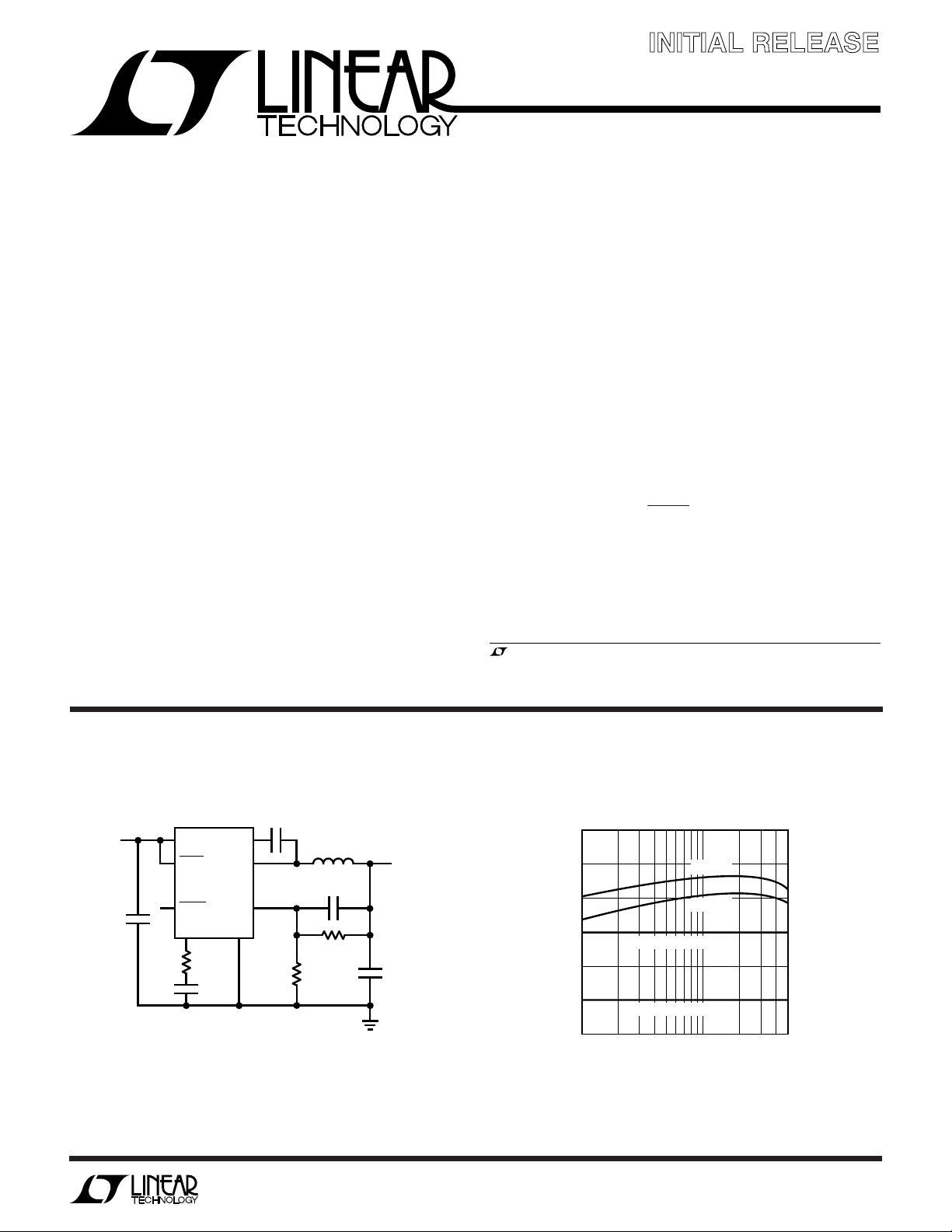
TYPICAL APPLICATION
The LT®1612 is an 800kHz, synchronous step-down DC/
DC converter that operates from an input voltage as low
as 2V. Internal 0.45Ω switches deliver output currents up
to 500mA, and the 800kHz switching frequency allows the
use of small, low value ceramic input and output capacitors. Input voltage ranges from 5.5V down to 2V and
output voltage can be set as low as the 620mV reference.
The device features Burst ModeTM operation, keeping
efficiency high at light loads. Burst Mode operation can be
defeated by pulling the MODE pin high, enabling constant
switching throughout the load range for low noise.
No-load quiescent current is 160µA and shutdown current
is less than 1µA. The device is available in 8-lead SO and
MSOP packages.
, LTC and LT are registered trademarks of Linear Technology Corporation.
Burst Mode is a trademark of Linear Technology Corporation.
V
IN
2V
C1
10µF
C1: TAIYO-YUDEN JMK325BJ106MN
C2: PANASONIC EEFCDOF680R
L1: SUMIDA CD43-100
V
IN
SHDN
MODE
V
C
BOOST
SW
LT1612
GND
33k
330pF
Figure 1. 2V to 1.2V Converter
Efficiency for LT1612 vs Linear Regulator
0.1µF
L1
10µH
100pF
FB
R1
215k
R2
232k
1%
Information furnished by Linear Technology Corporation is believed to be accurate and reliable.
However, no responsibility is assumed for its use. Linear Technology Corporation makes no representation that the interconnection of its circuits as described herein will not infringe on existing patent rights.
1%
V
1.2V
500mA
C2
68µF
3.15V
OUT
1612 F01a
90
80
70
60
EFFICIENCY (%)
50
40
30
V
= 1.2V
OUT
VIN = 2V (LINEAR)
VIN = 3V (LINEAR)
10010 500
LOAD CURRENT (mA)
VIN = 2V
VIN = 3V
1612 • F01b
1
LT1612
TOP VIEW
SHDN
MODE
BOOST
SW
V
C
FB
V
IN
GND
S8 PACKAGE
8-LEAD PLASTIC SO
1
2
3
4
8
7
6
5
WW
W
ABSOLUTE MAXIMUM RATINGS
U
(Note 1)
Supply Voltage (VIN)............................................... 5.5V
SW Pin Voltage....................................................... 5.5V
FB Pin Voltage ............................................... VIN + 0.3V
VC Pin Voltage ........................................................... 2V
SHDN Pin Voltage................................................... 5.5V
MODE Pin Voltage .................................................. 5.5V
U
W
U
PACKAGE/ORDER INFORMATION
ORDER PART
NUMBER
TOP VIEW
8
V
1
C
2
FB
3
V
IN
4
GND
MS8 PACKAGE
8-LEAD PLASTIC MSOP
T
= 125°C, θJA = 120°C/ W
JMAX
7
6
5
SHDN
MODE
BOOST
SW
LT1612EMS8
MS8 PART MARKING
LTMS
BOOST Pin Voltage ....................................... VIN + 5.5V
Junction Temperature...........................................125°C
Operating Temperature Range (Note 2) ... –40°C to 85°C
Storage Temperature Range ................. –65°C to 150°C
Lead Temperature (Soldering, 10 sec)..................300°C
ORDER PART
NUMBER
LT1612ES8
S8 PART MARKING
T
= 125°C, θJA = 120°C/W
JMAX
1612
Consult factory for Military grade parts.
ELECTRICAL CHARACTERISTICS
temperature range, otherwise specifications are TA = 25°C, V
SYMBOL PARAMETER CONDITIONS MIN TYP MAX UNITS
I
Q
V
FB
g
m
f
OSC
2
Quiescent Current MODE = 5V ● 12 mA
FB Voltage 0.605 0.62 0.635 V
FB Line Regulation ● 0.02 0.15 %/V
FB Pin Bias Current (Note 3) ● 750 nA
Error Amplifier Transconductance 250 µmhos
Min Input Voltage 2V
Max Input Voltage 5.5 V
Oscillator Frequency 700 800 900 kHz
f
Line Regulation 1%/V
OSC
Maximum Duty Cycle 85 90 %
Shutdown Threshold Minimum Voltage for Active
The ● denotes specifications which apply over the full operating
= V
IN
MODE = 0V, Not Switching
SHDN = 0V ● 1 µA
Maximum Voltage for Shutdown ● 0.2 V
SHDN
= 3V
● 160 220 µA
● 0.60 0.62 0.635 V
● 550 1100 kHz
● 80 %
● 2V
LT1612
ELECTRICAL CHARACTERISTICS
temperature range, otherwise specifications are TA = 25°C, V
SYMBOL PARAMETER CONDITIONS MIN TYP MAX UNITS
SHDN Pin Current SHDN = 2V
BOOST Pin Current BOOST = VIN + 2V 4 mA
Switch Current Limit (Note 4) Duty Cycle = 0% MODE = OV 600 710 900 mA
Burst Mode Operation Current Limit MODE = 0V 180 mA
Switch Voltage Drop ISW = 500mA 200 280 mV
Rectifier Voltage Drop I
SW Pin Leakage VSW = 5V ● 1 µA
Note 1: Absolute Maximum Ratings are those values beyond which the life
of a device may be impaired.
Note 2: The LT1612E is guaranteed to meet performance specifications
from 0°C to 70°C. Specifications over the –40°C to 85°C operating
The ● denotes specifications which apply over the full operating
= V
IN
SHDN = 5V ● 30 45 µA
= 500mA 300 400 mV
RECT
= 3V
SHDN
● 10 15 µA
MODE = 5V 550 650 900 mA
temperature range are assured by design, characterization and correlation
with statistical process controls.
Note 3: Bias current flows out of the FB pin.
Note 4: Duty cycle affects current limit due to slope compensation.
UUU
PIN FUNCTIONS
VC (Pin 1): Compensation Pin. This is the current sink/
source output of the error amplifier. By connecting an RC
network from this pin to ground, frequency response can
be tuned for a wide range of circuit configurations. The
voltage at this pin also sets the current limit, and if
grounded, the switch will remain in the OFF state.
FB (Pin 2): Feedback Pin. This pin is the negative input to
the error amplifier. Connect the resistor divider tap to this
point which sets V
V
= 0.62V (1 + R1/R2)
OUT
according to:
OUT
VIN (Pin 3): Supply Pin. Bypass capacitor C1 must be right
next to this pin.
GND (Pin 4): Ground Pin. Connect directly to local ground
plane.
SW (Pin 5): Switch Pin. Connect inductor and boost
capacitor here. Minimize trace area at this pin to keep EMI
down.
BOOST (Pin 6): This is the supply pin for the switch driver
and must be above VIN by 1.5V for proper switch operation. Connect the boost capacitor to this pin.
MODE (Pin 7): Burst Mode Operation Disable Pin. For
continuous switching operation (low noise), pull this pin
above 2V. For Burst Mode operation which gives better
light load efficiency, tie to ground. Output ripple voltage in
Burst Mode operation is typically 30mV
. See applica-
P-P
tions section for more information about this function.
SHDN (Pin 8): Shutdown Pin. Pull this pin low for shut-
down mode. Tie to a voltage between 2V and 5.5V for
normal operation.
3
 Loading...