

Linear Technology LT1610 Datasheet
FEATURES
■
Uses Tiny Capacitors and Inductor
■
Internally Compensated
■
Low Quiescent Current: 30µA
■
Operates with VIN as Low as 1V
■
3V at 30mA from a Single Cell
■
5V at 200mA from 3.3V
■
High Output Voltage Capability: Up to 28V
■
Low Shutdown Current: <1µA
■
Automatic Burst ModeTM Switching at Light Load
■
Low V
■
8-Lead MSOP and SO Packages
Switch: 300mV at 300mA
CESAT
U
APPLICATIO S
LT1610
1.7MHz, Single Cell
Micropower
DC/DC Converter
U
DESCRIPTIO
The LT®1610 is a micropower fixed frequency DC/DC
converter that operates from an input voltage as low as 1V.
Intended for small, low power applications, it switches at
1.7MHz, allowing the use of tiny capacitors and inductors.
The device can generate 3V at 30mA from a single cell
(1V) supply. An internal compensation network can be
connected to the LT1610’s VC pin, eliminating two external components. No-load quiescent current of the LT1610
is 30µA, and the internal NPN power switch handles a
300mA current with a voltage drop of 300mV.
The LT1610 is available in 8-lead MSOP and SO packages.
■
Pagers
■
Cordless Phones
■
Battery Backup
■
LCD Bias
■
Portable Electronic Equipment
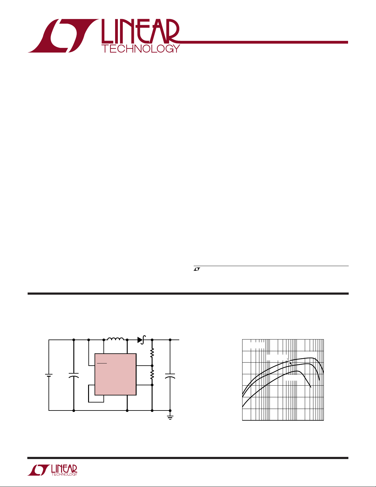
TYPICAL APPLICATIO
L1
4.7µH
65
V
IN
3
C1
22µF
SHDN
LT1610
8
V
C
1
+
1 CELL
C1, C2: AVX TAJA226M006R
D1: MOTOROLA MBR0520
L1: MURATA LQH1C4R7
Figure 1. 1-Cell to 3V Step-Up Converter
U
SW
GNDCOMP
PGND
, LTC and LT are registered trademarks of Linear Technology Corporation.
Burst Mode is a trademark of Linear Technology Corporation.
D1
R1
1M
2
FB
R2
681k
7
4
V
OUT
3V
30mA
+
C2
22µF
1610 F01
85
V
OUT
80
75
70
65
EFFICIENCY (%)
60
55
50
0.1
Efficiency
= 3V
VIN = 1.25V
VIN = 1V
1 10 100
LOAD CURRENT (mA)
VIN = 1.5V
1610 TA01
1
LT1610
1
2
3
4
8
7
6
5
TOP VIEW
V
C
FB
SHDN
PGND
COMP
GND
V
IN
SW
S8 PACKAGE
8-LEAD PLASTIC SO
WW
W
U
ABSOLUTE MAXIMUM RATINGS
(Note 1)
VIN Voltage ................................................................ 8V
SW Voltage ............................................... –0.4V to 30V
FB Voltage ..................................................... VIN + 0.3V
VC Voltage ................................................................ 2V
COMP Voltage .......................................................... 2V
Current into FB Pin .............................................. ±1mA
SHDN Voltage ............................................................ 8V
U
W
U
PACKAGE/ORDER INFORMATION
ORDER PART
TOP VIEW
V
1
C
2
FB
3
SHDN
4
PGND
MS8 PACKAGE
8-LEAD PLASTIC MSOP
T
= 125°C, θJA = 160°C/W
JMAX
8
7
6
5
COMP
GND
V
IN
SW
NUMBER
LT1610CMS8
MS8 PART MARKING
LTDT
Maximum Junction Temperature ......................... 125°C
Operating Temperature Range (Note 1)
Commercial .............................................0°C to 70°C
Extended Commercial (Note 2).......... –40°C to 85°C
Industrial ........................................... –40°C to 85°C
Storage Temperature Range ................. –65°C to 150°C
Lead Temperature (Soldering, 10 sec).................. 300°C
ORDER PART
NUMBER
LT1610CS8
LT1610IS8
S8 PART MARKING
1610
T
= 125°C, θJA = 120°C/W
JMAX
1610I
Consult factory for Military grade parts.
LECTRICAL C CHARA TERIST
E
range, otherwise specifications are at T
= 25°C. Commercial grade 0°C to 70°C, V
A
ICS
The ● denotes specifications which apply over the specified temperature
= 1.5V, V
IN
= VIN, unless otherwise noted.
SHDN
(Note 2)
PARAMETER CONDITIONS MIN TYP MAX UNITS
Minimum Operating Voltage 0.9 1 V
Maximum Operating Voltage 8V
Feedback Voltage ● 1.20 1.23 1.26 V
Quiescent Current V
Quiescent Current in Shutdown V
FB Pin Bias Current ● 27 80 nA
Reference Line Regulation 1V ≤ VIN ≤ 2V (25°C, 0°C) 0.6 1 %/V
Error Amp Transconductance ∆I = 2µA25µmhos
Error Amp Voltage Gain 100 V/V
Switching Frequency ● 1.4 1.7 2 MHz
Maximum Duty Cycle 77 80 95 %
= 1.5V, Not Switching 30 60 µA
SHDN
= 0V, VIN = 2V 0.01 0.5 µA
SHDN
= 0V, VIN = 5V 0.01 1.0 µA
V
SHDN
≤ 2V (70°C) 2 %/V
1V ≤ V
IN
2V ≤ V
≤ 8V (25°C, 0°C) 0.03 0.15 %/V
IN
≤ 8V (70°C) 0.2 %/V
2V ≤ V
IN
● 75 95 %
2
LT1610
LECTRICAL C CHARA TERIST
E
range, otherwise specifications are at T
= 25°C. Commercial grade 0°C to 70°C, V
A
ICS
The ● denotes specifications which apply over the specified temperature
= 1.5V, V
IN
= VIN, unless otherwise noted.
SHDN
(Note 2)
PARAMETER CONDITIONS MIN TYP MAX UNITS
Switch Current Limit (Note 3) 450 600 900 mA
Switch V
CESAT
Switch Leakage Current VSW = 5V 0.01 1 µA
SHDN Input Voltage High 1V
SHDN Input Voltage Low 0.3 V
SHDN Pin Bias Current V
ISW = 300mA 300 350 mV
● 400 mV
= 3V 10 µA
SHDN
= 0V 0.01 0.1 µA
V
SHDN
The ● denotes specifications which apply over the specified temperature range, otherwise specifications are at TA = 25°C.
Industrial grade –40°C to 85°C, V
PARAMETER CONDITIONS MIN TYP MAX UNITS
Minimum Operating Voltage TA = 85°C 0.9 1 V
Maximum Operating Voltage 8V
Feedback Voltage ● 1.20 1.23 1.26 V
Quiescent Current 30 60 µA
Quiescent Current in Shutdown V
FB Pin Bias Current ● 27 80 nA
Reference Line Regulation 2V ≤ VIN ≤ 8V (–40°C) 0.03 0.15 %/V
Error Amp Transconductance ∆I = 2µA25µmhos
Error Amp Voltage Gain 100 V/V
Switching Frequency (Note 4) ● 1.4 1.7 2 MHz
Maximum Duty Cycle (Note 4) 77 80 95 %
Switch Current Limit 450 600 900 mA
Switch V
CESAT
Switch Leakage Current VSW = 5V 0.01 1 µA
SHDN Input Voltage High 1V
SHDN Input Voltage Low 0.3 V
SHDN Pin Bias Current V
= 1.5V, V
IN
= VIN, unless otherwise noted.
SHDN
= –40°C 1.25 V
T
A
= 0V, VIN = 2V 0.01 0.5 µA
SHDN
= 0V, VIN = 5V 0.01 1.0 µA
V
SHDN
≤ 8V (85°C) 0.2 %/V
2V ≤ V
IN
● 75 95 %
ISW = 300mA 300 350 mV
● 400 mV
= 3V 10 µA
SHDN
V
= 0V 0.01 0.1 µA
SHDN
Note 1: Absolute Maximum Ratings are those values beyond which the life
of a device may be impaired.
Note 2: The LT1610C is guaranteed to meet specified performance from
0°C to 70°C and is designed, characterized and expected to meet these
extended temperature limits, but is not tested at –40°C and 85°C. The
LT1610I is guaranteed to meet the extended temperature limits.
Note 3: Current limit guaranteed by design and/or correlation to static test.
Current limit is affected by duty cycle due to ramp generator. See Block
Diagram.
Note 4: Not 100% tested at 85°C.
3

LT1610
UW
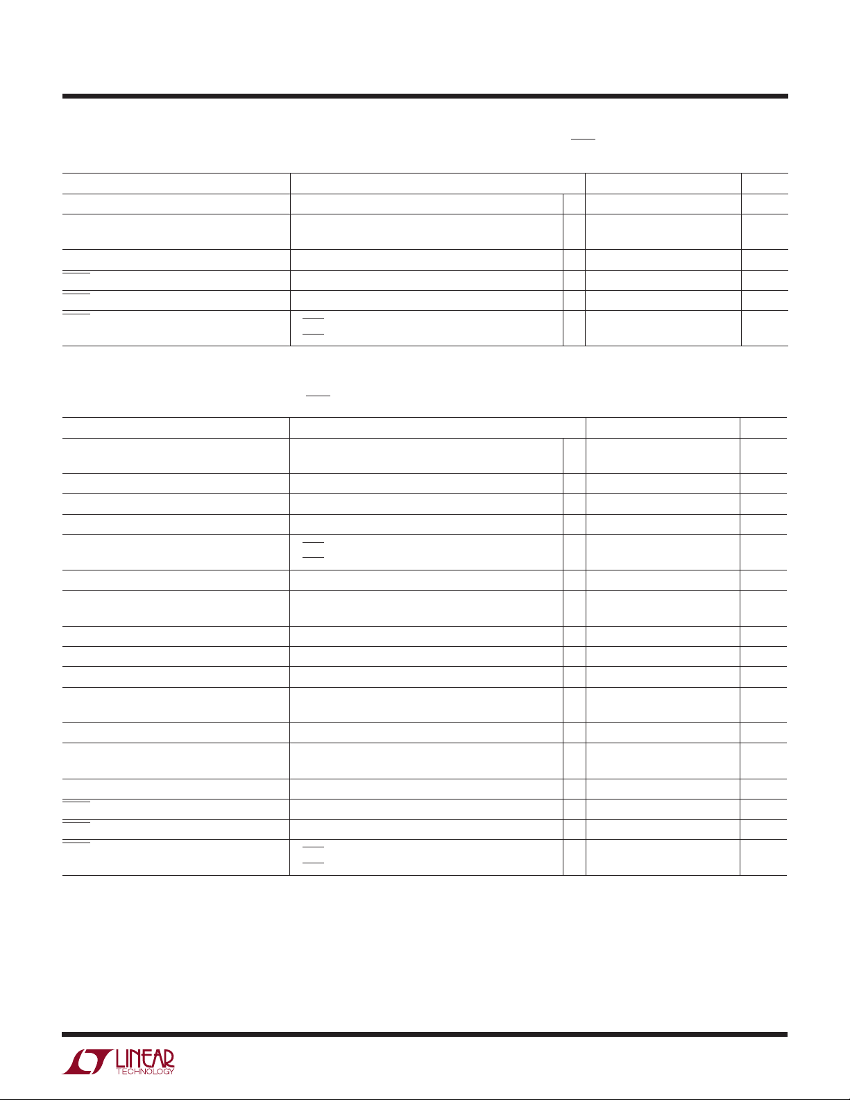
TYPICAL PERFOR A CE CHARACTERISTICS
Current Limit (DC = 30%)
600
500
400
(mV)
CESAT
300
V
200
100
CESAT
0
vs Current
TA = 25°C
200 300 400
100
SWITCH CURRENT (mA)
TA = 85°C
= –40°C
T
A
500 600
1610 G01
vs Temperature
800
700
600
500
400
SWITCH CURRENT LIMIT (mA)
300
200
–50
02550
–25
TEMPERATURE (°C)
75 100
1610 G02
Current Limit vs Duty CycleV
800
700
600
500
400
300
CURRENT LIMIT (mA)
200
100
0
20 40 60 1007010 30 50 90
0
TA = 25°C
80
DUTY CYCLE (%)
1610 G03
Oscillator Frequency
vs Input Voltage Feedback Voltage
2.50
TA = 25°C
2.25
2.00
1.75
1.50
1.25
1.00
0.75
0.50
SWITCHING FREQUENCY (MHz)
0.25
0
0
13
2
INPUT VOLTAGE (V)
SHDN Pin Current
vs SHDN Pin Voltage
50
40
30
20
SHDN CURRENT (µA)
10
7
4
6
5
1610 G04
1.240
1.235
1.230
1.225
1.220
FEEDBACK VOLTAGE (V)
1.215
1.210
8
V
OUT
50mV/DIV
AC COUPLED
100mA/DIV
31mA
I
LOAD
1mA
–50
–25
Transient Response,
Circuit of Figure 1
I
L1
VIN = 1.25V 500µs/DIV
V
= 3V
OUT
02550
TEMPERATURE (°C)
75 100
1610 G05
1610 TA08
40
35
30
25
20
15
10
QUIESCENT CURRENT (µA)
V
OUT
20mV/DIV
AC COUPLED
SWITCH
VOLTAGE
2V/DIV
SWITCH
CURRENT
50mA/DIV
Quiescent Current
vs Temperature
5
0
–25 0 50
–50
25
TEMPERATURE (°C)
Burst Mode Operation,
Circuit of Figure 1
= 1.25V 20µs/DIV
V
IN
= 3V
V
OUT
= 3mA
I
LOAD
75
100
1610 G06
1610 TA08
4
0
0
12
SHDN VOLTAGE (V)
4
35 8
67
1610 G07
UUU
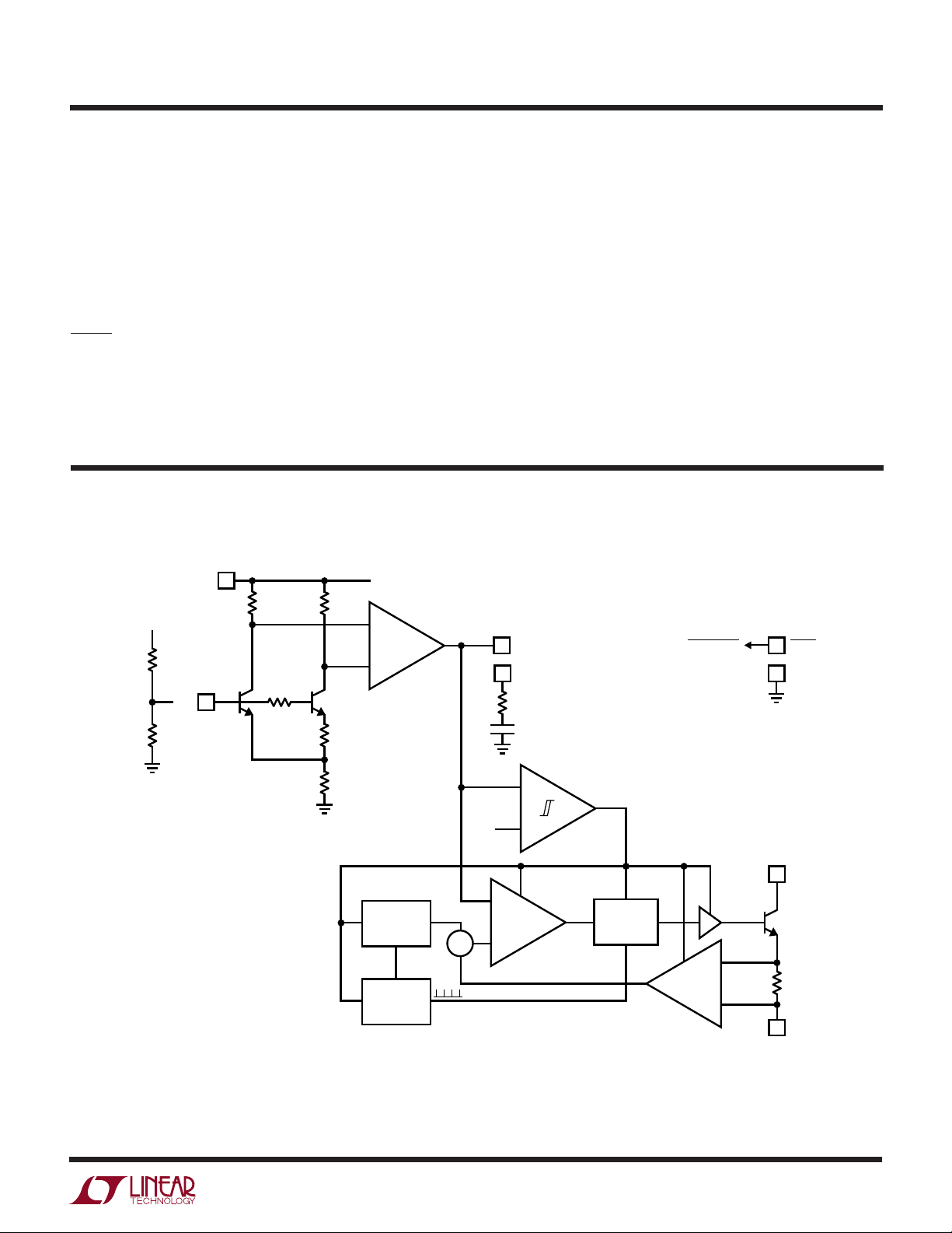
PIN FUNCTIONS
LT1610
VC (Pin 1): Error Amplifier Output. Frequency compensation network must be connected to this pin, either internal
(COMP pin) or external series RC to ground. 220kΩ/
220pF typical value.
FB (Pin 2): Feedback Pin. Reference voltage is 1.23V.
Connect resistive divider tap here. Minimize trace area at
FB. Set V
according to V
OUT
= 1.23V (1 + R1/R2).
OUT
SHDN (Pin 3): Shutdown. Ground this pin to turn off
device. Tie to 1V or more to enable.
PGND (Pin 4): Power Ground. Tie directly to local ground
plane.
W
BLOCK DIAGRA
V
IN
V
OUT
R1
(EXTERNAL)
R2
(EXTERNAL)
6
R5
40k
Q1
FB
2
FB
Q2
× 10
R6
40k
R3
30k
V
IN
+
A1
g
m
–
SW (Pin 5): Switch Pin. Connect inductor/diode here.
Minimize trace area at this pin to keep EMI down.
VIN (Pin 6): Input Supply Pin. Must be locally bypassed.
GND (Pin 7): Signal Ground. Carries all device ground
current except switch current. Tie to local ground plane.
COMP (Pin 8): Internal Compensation Network. Tie to V
C
pin, or let float if external compensation is used. Output
capacitor must be tantalum if COMP pin is used for compensation.
1
V
C
COMP
8
R
C
C
C
3
SHDNSHUTDOWN
GND
7
R4
140k
+
BIAS
RAMP
GENERATOR
Σ
1.7MHz
OSCILLATOR
–
A2
+
–
COMPARATOR
Figure 2. LT1610 Block Diagram
ENABLE
FF
RQ
S
A = 3
DRIVER
+
–
5
Q3
4
SW
0.15Ω
PGND
1610 F02
5
 Loading...