

Linear Technology LT1585-1.5, LT1585A-1.5 Datasheet

FEATURES
LT1585-1.5/LT1585A-1.5
Fixed 1.5V, 4.6A and 5A
Low Dropout, Fast Response
GTL+ Regulators
U
DESCRIPTIO
■
Fast Transient Response
■
Guaranteed Dropout Voltage at Multiple Currents
■
Load Regulation: 0.05% Typ
■
Trimmed Current Limit
■
On-Chip Thermal Limiting
U
APPLICATIO S
■
GTL+ Power Supply
■
Low Voltage Logic Supplies
■
Battery-Powered Circuitry
U
TYPICAL APPLICATIO
The LT®1585-1.5/LT1585A-1.5 are low dropout, 3-terminal regulators with 4.6A and 5A output current capability
respectively, and a fixed 1.5V output voltage. The designs
are optimized for low voltage applications where transient
response and minimum input voltage are critical. Similar to
the LT1084, they have lower dropout and faster transient
response. These improvements make them ideal for low
voltage microprocessor applications, especially as the
regulator in an Intel processor GTL+ supply.
Current limit is trimmed to ensure specified output current
and controlled short-circuit current. On-chip thermal limiting provides protection against any combination of overload that creates excessive junction temperatures.
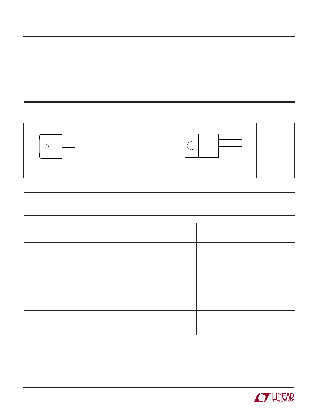
The LT1585-1.5/LT1585A-1.5 are available in the throughhole 3-pin TO-220 power package and 3-pin plastic DD.
, LTC and LT are registered trademarks of Linear Technology Corporation.
3.3V
LT1585A-1.5
V
C1, C2
+
100µF
10V
NOTE: LTC RECOMMENDS CENTRALLY
LOCATING THE LT1585A-1.5 TO MINIMIZE
DISTRIBUTION DROPS AND USING
V
TT
SEPARATE V
BUS END
V
IN
OUT
GND
GENERATORS AT EACH
REF
+
V
5A
TT
= 1.5V
C3 TO C6
100µF
10V
Intel Processor GTL+ Supply
C7 TO
C12
1µF
RX
TX
RX
R1
75Ω
V
REF
R2
150Ω
TX
C13
0.1µF
Q1
Q3
R5
100ΩR7100ΩR8100ΩR6100Ω
•
•
•
142 TOTAL SIGNAL LINES
R3
V
75Ω
REF
R4
150Ω
Q2
Q4
C14
0.1µF
RX
TX
RX
TX
1585-1.5 • TA01
1
LT1585-1.5/LT1585A-1.5
WW
W
ABSOLUTE MAXIMUM RATINGS
U
(Note 1)
VIN............................................................................ 7V
Operating Junction Temperature Range
Control Section .................................. 0°C to 125°C
Power Transistor ................................ 0°C to 150°C
U
W
PACKAGE/ORDER INFORMATION
FRONT VIEW
TAB
IS
OUTPUT
Consult factory for Industrial and Military grade parts.
3
2
1
M PACKAGE
3-LEAD PLASTIC DD
θJA = 30°C/W*
*WITH PACKAGE
SOLDERED TO 0.5
V
IN
SQUARE INCH COPPER
AREA OVER BACKSIDE
V
OUT
GROUND PLANE OR
INTERNAL POWER PLANE.
GND
CAN VARY FROM
θ
JA
20°C/W TO >40°C/W
WITH OTHER MOUNTING
TECHNIQUES
ORDER PART
NUMBER
LT1585CM-1.5
LT1585ACM-1.5
Storage Temperature Range ................ –65°C to 150°C
Lead Temperature (Soldering, 10 sec)................. 300°C
UUU
PRECONDITIONI G
100% Thermal Limit Functional Test
U
ORDER PART
IN
OUT
LT1585CT-1.5
LT1585ACT-1.5
TAB IS
OUTPUT
FRONT VIEW
3
2
1
T PACKAGE
3-LEAD PLASTIC TO-220
θJA = 50°C/W
V
V
GND
NUMBER
ELECTRICAL CHARACTERISTICS
The ● denotes specifications which apply over the specified operating
temperature range, otherwise specifications are at TA = 25°C.
PARAMETER CONDITIONS MIN TYP MAX UNITS
Output Voltage (Note 4) VIN = 5V, TJ = 25°C, I
Line Regulation (Notes 2, 3) 3V ≤ VIN ≤ 7V, I
Load Regulation VIN = 5V, TJ = 25°C, 0mA ≤ I
(Notes 2, 3, 4) ● 0.05 0.5 %
Dropout Voltage (Note 4) ∆V
Current Limit LT1585-1.5, (V
Quiescent Current V
Ripple Rejection (Note 4) f = 120Hz, C
Thermal Regulation TA = 25°C, 30ms Pulse 0.004 0.02 %/W
Temperature Stability ● 0.5 %
Long-Term Stability TA = 125°C, 1000 Hrs. 0.03 1.0 %
RMS Output Noise TA = 25°C, 10Hz ≤ f ≤ 10kHz 0.003 %
(% of V
Thermal Resistance T Package: Control Circuitry/Power Transistor 0.7/3.0 °C/W
Junction to Case M Package: Control Circuitry/Power Transistor 0.7/3.0 °C/W
Note 1: Absolute Maximum Ratings are those values beyond which the life
of the device may be impaired.
Note 2: See thermal regulation specifications for changes in output voltage
due to heating effects. Load and line regulation are measured at a constant
junction temperature by low duty cycle pulse testing.
Note 3: Line and load regulation are guaranteed up to the maximum
power dissipation (25W for the LT1585-1.5 in T package and 27.5W for
OUT
)
≤ 7V, 0mA ≤ I
3V ≤ V
IN
= 1%, I
OUT
LT1585A-1.5, (V
= 5V ● 713 mA
IN
OUT
IN
OUT
= 0mA 1.485 (–1%) 1.5 1.515 (+1%) V
OUT
≤ I
OUT
FULL LOAD
= 0mA 0.005 0.2 %
OUT
≤ I
OUT
FULL LOAD
= I
FULL LOAD
– V
) = 5.5V ● 4.60 5.25 A
OUT
– V
IN
= 25µF Tant., VIN = 4.5V, I
) = 5.5V ● 5.00 6.00 A
OUT
= I
OUT
FULL LOAD
the LT1585A-1.5). Power dissipation is determined by input/output
differential and the output current. Guaranteed maximum output power
will not be available over the full input/output voltage range.
Note 4: I
FULL LOAD
as a function of input-to-output voltage. I
LT1585-1.5 and 5A for the LT1585A-1.5. The LT1585-1.5/LT1585A-1.5
have constant current limit with changes in input-to-output voltage.
● 1.470 (–2%) 1.5 1.530 (+2%) V
0.05 0.3 %
● 1.200 1.400 V
● 60 72 dB
is defined as the maximum value of output load current
FULL LOAD
is equal to 4.6A for the
2
W
TEMPERATURE (°C)
–0.20
OUTPUT VOLTAGE DEVIATION (%)
–0.10
0
0.10
–0.15
–0.05
0.05
–25 25 75 125
1585-1.5 G03
175–50–75 0 50 100 150
∆I = I
FULL LOAD
U
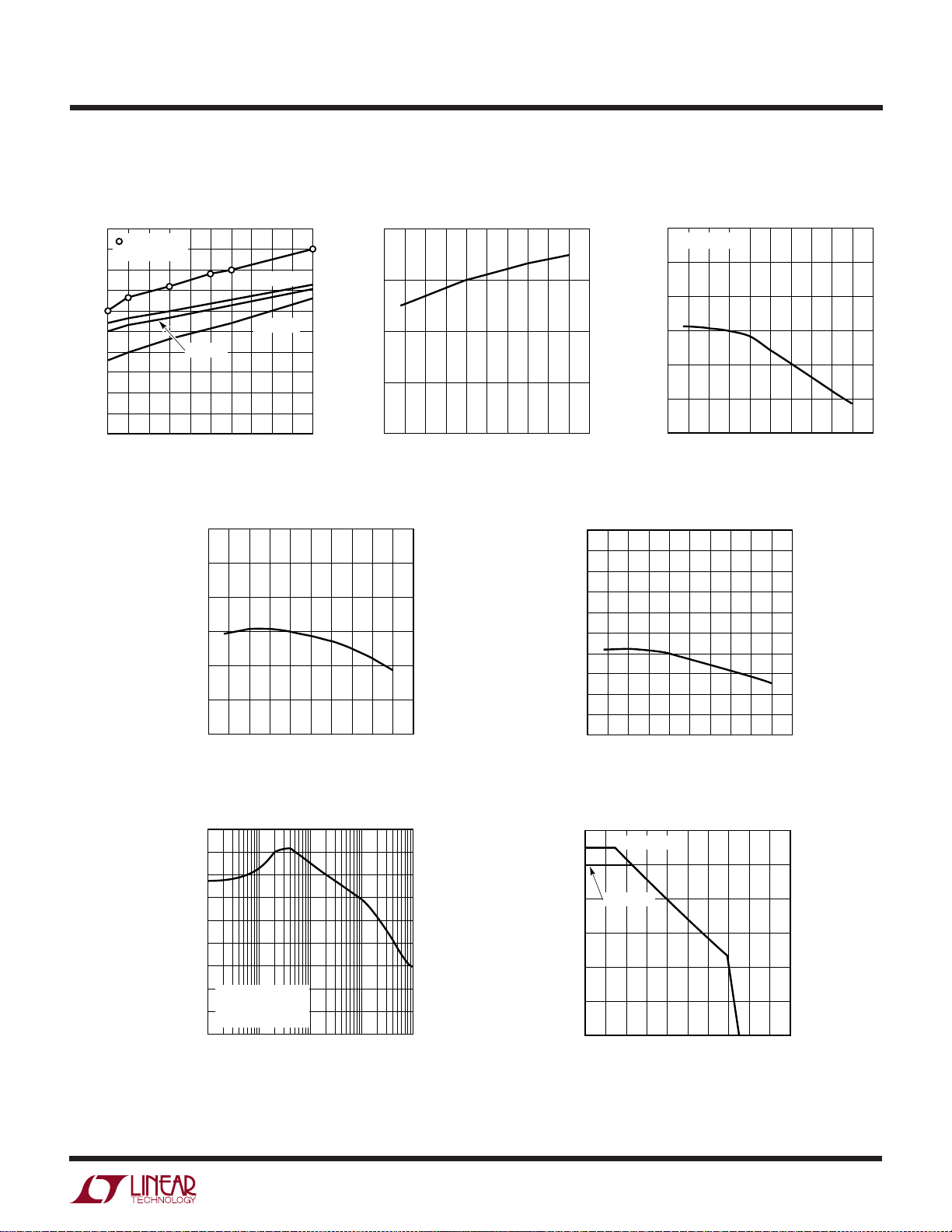
TYPICAL PERFORMANCE CHARACTERISTICS
LT1585-1.5/LT1585A-1.5
LT1585A-1.5 Dropout Voltage vs
Output Current
1.5
GUARANTEED
1.4
TEST POINTS
1.3
1.2
1.1
1.0
0.9
0.8
DROPOUT VOLTAGE (V)
0.7
0.6
0.5
0
T = 25°C
1
2
OUTPUT CURRENT (A)
3
Output Voltage vs Temperature
1.53
1.52
1.51
1.50
1.49
OUTPUT VOLTAGE (V)
1.48
1.47
–25 25 75 125
T = –5°C
T = 125°C
4
5
1585-1.5 G01
TEMPERATURE (°C)
LT1585A-1.5 Short-Circuit Current
vs Temperature
6.0
5.5
5.0
4.5
SHORT-CIRCUIT CURRENT (A)
4.0
–50
–75
1585-1.5 G04
–25
175–50–75 0 50 100 150
50
75
0
25
TEMPERATURE (°C)
100
Load Regulation vs Temperature
125
175
150
1585-1.5 G02
Quiescent Current vs Temperature
13
12
11
10
9
8
7
6
QUIESCENT CURRENT (mA)
5
4
3
–25
0
–50 150
–75
25
50
TEMPERATURE (°C)
75
100
125
175
1585-1.5 G05
Ripple Rejection vs Frequency
90
80
70
60
50
40
30
RIPPLE REJECTION (dB)
20
(VIN – V
0.5V ≤ V
10
I
OUT
0
10 1k 10k 100k
OUT
= I
FULL LOAD
100
RIPPLE
) ≤ 3V
≤ 2V
FREQUENCY (Hz)
1585-1.5 G06
Maximum Power Dissipation*
30
25
20
15
POWER (W)
10
5
0
*AS LIMITED BY MAXIMUM JUNCTION TEMPERATURE
50
LT1585A-1.5
LT1585-1.5
90 110 120 130 140 150
80 100
60 70
CASE TEMPERATURE (˚C)
1585-1.5 G07
3
 Loading...