

Linear Technology LT1585, LT1584, LT1587 Datasheet
LT1584/LT1585/LT1587
FEATURES
■
Fast Transient Response
■
Guaranteed Dropout Voltage at Multiple Currents
■
Load Regulation: 0.05% Typ
■
Trimmed Current Limit
■
On-Chip Thermal Limiting
■
Standard 3-Pin Power Package
U
APPLICATIONS
■
PentiumTM Processor Supplies
■
PowerPCTM Supplies
■
Other 2.5V to 3.6V Microprocessor Supplies
■
Low Voltage Logic Supplies
■
Battery-Powered Circuitry
■
Post Regulator for Switching Supply
LT1585/7CM, LT1584/5/7CT Adjustable
LT1585/7CM-3.3, LT1584/5/7CT-3.3 3.3V Fixed
LT1585CM-3.38, LT1584/5CT-3.38 3.38V Fixed
LT1585/7CM-3.45, LT1584/5/7CT-3.45 3.45V Fixed
LT1585/7CM-3.6, LT1584/5/7CT-3.6 3.6V Fixed
7A, 4.6A, 3A Low Dropout
Fast Response
Positive Regulators
Adjustable and Fixed
U
DESCRIPTION
The LT®1584/LT1585/LT1587 are low dropout threeterminal regulators with 7A, 4.6A and 3A output current
capability, respectively. Design has been optimized for low
voltage applications where transient response and minimum input voltage are critical. Similar to the LT1083/4/5
family, it has lower dropout voltage and faster transient
response. These improvements make it ideal for low voltage microprocessor applications requiring a regulated
2.5V to 3.6V output with an input supply below 7V.
Current limit is trimmed to ensure specified output current
and controlled short-circuit current. On-chip thermal limiting provides protection against any combination of overload that would create excessive junction temperatures.
The LT1585/LT1587 are available in both the through-hole
and surface mount versions of the industry standard 3-pin
TO-220 power package. The LT1584 is available in the
through-hole 3-pin TO-220 power package.
, LTC and LT are registered trademarks of Linear Technology Corporation.
Pentium is a trademark of Intel Corporation. PowerPC is a trademark of IBM Corporation.
U
TYPICAL APPLICATION
3.3V, 7A, 4.6A, 3A Regulator
LT1584-3.3
≥ 4.75V
V
IN
* REQUIRED FOR STABILITY
LT1584: C2 = 22µF,
LT1585/LT1587: C2 = 10µF
NOTE: MICROPROCESSOR APPLICATIONS WITH LOAD TRANSIENTS OF 3.8A REQUIRE
OUTPUT DECOUPLING CAPACITANCE > 1300µF ON FIXED VOLTAGE PARTS TO ACHIEVE
< 50mV OF DEVIATION FROM NOMINAL OUTPUT. CONSULT FACTORY FOR DETAILS
+
C1
10µF
LT1585-3.3
LT1587-3.3
+
3.3V
7A, 4.6A, 3A
C2*
SOLID
TANTALUM
1585 TA01
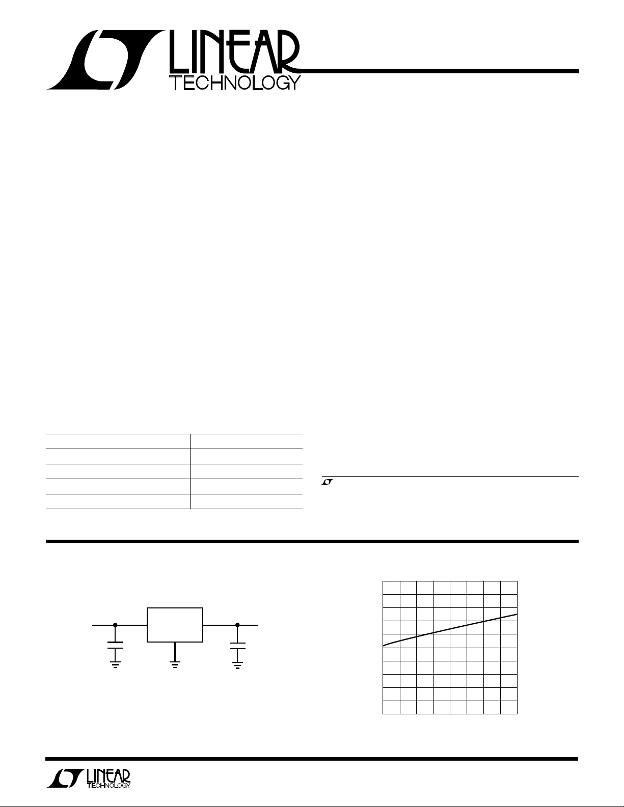
Dropout Voltage vs Output Current
1.5
1.4
1.3
1.2
1.1
1.0
0.9
0.8
0.7
INPUT/OUTPUT DIFFERENTIAL (V)
0.6
0.5
0
OUTPUT CURRENT (A)
I
FULL LOAD
1585 TA02
1

LT1584/LT1585/LT1587
WW
W
U
ABSOLUTE MAXIMUM RATINGS
VIN............................................................................. 7V
Operating Junction Temperature Range
Control Section.................................... 0°C to 125°C
Power Transistor ................................. 0°C to 150°C
U
W
PACKAGE/ORDER INFORMATION
FRONT VIEW
3
2
1
M PACKAGE
3-LEAD PLASTIC DD PAK
θJA = 30°C/W* θJA = 50°C/W
FRONT VIEW
3
2
1
VIN
V
OUT
ADJ
VIN
V
OUT
GND
ORDER PART
NUMBER
LT1585CM
LT1587CM
LT1585CM-3.3
LT1585CM-3.38
LT1585CM-3.45
LT1585CM-3.6
LT1587CM-3.3
M PACKAGE
3-LEAD PLASTIC DD PAK
θJA = 30°C/W* θJA = 50°C/W
LT1587CM-3.45
LT1587CM-3.6
FRONT VIEW
T PACKAGE
3-LEAD PLASTIC TO-220
FRONT VIEW
T PACKAGE
3-LEAD PLASTIC TO-220
Storage Temperature Range ................. –65°C to 150°C
Lead Temperature (Soldering, 10 sec).................. 300°C
UUU
PRECONDITIONI G
100% Thermal Limit Functional Test
U
ORDER PART
3
2
1
3
2
1
VIN
V
OUT
ADJ
VIN
V
OUT
GND
LT1584CT-3.3
LT1585CT-3.3
LT1587CT-3.3
LT1584CT-3.38
LT1585CT-3.38
NUMBER
LT1584CT
LT1585CT
LT1587CT
LT1584CT-3.45
LT1585CT-3.45
LT1587CT-3.45
LT1584CT-3.6
LT1585CT-3.6
LT1587CT-3.6
* With package soldered to 0.5 square inch copper area over backside
ground plane or internal power plane. θ
>40°C/W with other mounting techniques.
can vary from 20°C/W to
JA
Consult factory for Industrial and Military grade parts.
ELECTRICAL CHARACTERISTICS
PARAMETER CONDITIONS MIN TYP MAX UNITS
Reference Voltage LT1584 1.5V ≤ (VIN – V
LT1585 1.5V ≤ (VIN – V
LT1587 1.5V ≤ (V
Output Voltage LT1584-3.3 4.75V ≤ VIN ≤ 6.3V, 0mA ≤ I
LT1585-3.3 4.75V ≤ VIN ≤ 7V, 0mA ≤ I
LT1587-3.3 4.75V ≤ VIN ≤ 7V, 0mA ≤ I
LT1584-3.38 4.75V ≤ VIN ≤ 6.38V, 0mA ≤ I
LT1585-3.38 4.75V ≤ VIN ≤ 7V, 0mA ≤ I
LT1584-3.45 4.75V ≤ VIN ≤ 6.45V, 0mA ≤ I
LT1585-3.45 4.75V ≤ VIN ≤ 7V, 0mA ≤ I
LT1587-3.45 4.75V ≤ VIN ≤ 7V, 0mA ≤ I
LT1584-3.6 4.75V ≤ VIN ≤ 7V, 0mA ≤ I
LT1584-3.6 4.80V ≤ VIN ≤ 7V, 0mA ≤ I
LT1584-3.6 4.80V ≤ VIN ≤ 6.6V, 0mA ≤ I
LT1584-3.6 4.85V ≤ V
1.5V ≤ (VIN – V
IN
4.75V ≤ V
) ≤ 3V, 10mA ≤ I
OUT
) ≤ 5.75V, 10mA ≤ I
OUT
) ≤ 5.75V, 10mA ≤ I
OUT
– V
) ≤ 5.75V, 10mA ≤ I
OUT
≤ 7V, 0mA ≤ I
IN
≤ 6.6V, 0mA ≤ I
IN
≤ 7A
OUT
≤ 4.6A, TJ ≥ 25°C
OUT
≤ 4A, TJ < 25°C
OUT
≤ 3A ● 1.225 (– 2%) 1.250 1.275 (+2%) V
OUT
≤ 7A
OUT
≤ 4.6A, TJ ≥ 25°C
OUT
≤ 4A, TJ < 25°C
OUT
≤ 3A ● 3.235 (– 2%) 3.300 3.365 (+2%) V
OUT
≤ 7A
OUT
≤ 4A ● 3.313 (– 2%) 3.380 3.465 (+2.5%) V
OUT
≤ 7A
OUT
≤ 4A
OUT
≤ 3A ● 3.381 (– 2%) 3.450 3.519 (+2%) V
OUT
≤ 6A ● 3.400 (– 5.5%) 3.600 3.672 (+2%) V
OUT
≤ 6A ● 3.450 (– 4%) 3.600 3.672 (+2%) V
OUT
≤ 7A ● 3.431 (– 4.7%) 3.600 3.672 (+ 2%) V
OUT
≤ 7A ● 3.481 (– 3.3%) 3.600 3.672 (+ 2%) V
OUT
2

LT1584/LT1585/LT1587
ELECTRICAL CHARACTERISTICS
PARAMETER CONDITIONS MIN TYP MAX UNITS
Output Voltage LT1585/7-3.6 4.75V ≤ VIN ≤ 7V, 0mA ≤ I
LT1585/7-3.6 4.80V ≤ VIN ≤ 7V, 0mA ≤ I
LT1585-3.6 4.80V ≤ VIN ≤ 7V, 0mA ≤ I
LT1585-3.6 4.85V ≤ V
Line Regulation LT1584/5/7 2.75V ≤ VIN ≤ 7V, I
(Notes 1, 2) LT1584/5/7-3.3 4.75V ≤ VIN ≤ 7V, I
LT1584/5-3.38 4.75V ≤ VIN ≤ 7V, I
LT1584/5/7-3.45 4.75V ≤ V
LT1584/5/7-3.6 4.75V ≤ VIN ≤ 7V, I
Load Regulation LT1584/5/7 (VN – V
≤ 7V, 0mA ≤ I
IN
OUT
OUT
OUT
≤ 7V, I
IN
OUT
OUT
OUT
) = 3V, TJ = 25°C, 10mA ≤ I
(Notes 1, 2, 3) LT1584/5/7-3.3 VIN = 5V, TJ = 25°C, 0mA ≤ I
LT1584/5-3.38 VIN = 5V, TJ = 25°C, 0mA ≤ I
LT1584/5/7-3.45 VIN = 5V, TJ = 25°C, 0mA ≤ I
LT1584/5/7-3.6 VIN = 5.25V, TJ = 25°C, 0mA ≤ I
Dropout Voltage LT1585/7 ∆V
LT1585/7-3.3 ∆V
LT1585-3.38 ∆V
LT1585/7-3.45 ∆V
LT1585/7-3.6 ∆V
LT1585 ∆V
LT1585-3.3 ∆V
LT1585-3.38 ∆V
LT1585-3.45 ∆V
LT1585-3.6 ∆V
LT1584 ∆V
LT1584-3.3 ∆V
LT1584-3.38 ∆V
LT1584-3.45 ∆V
LT1584-3.6 ∆V
= 1%, I
REF
= 1%, I
OUT
= 1%, I
OUT
= 1%, I
OUT
= 1%, I
OUT
= 1%, I
REF
∆V
= 1%, I
REF
= 1%, I
OUT
∆V
= 1%, I
OUT
= 1%, I
OUT
= 1%, I
OUT
= 1%, I
OUT
= 1%, I
REF
= 1%, I
OUT
= 1%, I
OUT
= 1%, I
OUT
= 1%, I
OUT
T
≥ 25°C ● 1.200 1.300 V
J
= 3A
OUT
= 3A
OUT
= 3A
OUT
= 3A
OUT
= 3A ● 1.150 1.300 V
OUT
= 4.6A, TJ ≥ 25°C
OUT
= 4A, TJ < 25°C
OUT
= 4.6A, TJ ≥ 25°C
OUT
= 4A, TJ < 25°C
OUT
= 4A
OUT
= 4A
OUT
= 4A ● 1.200 1.400 V
OUT
= 6A
OUT
= 6A
OUT
= 6A
OUT
= 6A
OUT
= 6A
OUT
TJ < 25°C ● 1.200 1.350 V
LT1584 ∆V
LT1584-3.3 ∆V
LT1584-3.38 ∆V
LT1584-3.45 ∆V
LT1584-3.6 ∆V
Current Limit LT1584 (VIN – V
(Note 3) LT1584-3.3 (VIN – V
LT1584-3.38 (VIN – V
LT1584-3.45 (V
LT1584-3.6 (VIN – V
LT1585 (VIN – V
LT1585-3.3 (V
IN
IN
REF
OUT
OUT
OUT
OUT
– V
– V
= 1%, I
= 1%, I
= 1%, I
= 1%, I
= 1%, I
OUT
OUT
OUT
OUT
OUT
OUT)
OUT)
= 7A
OUT
= 7A
OUT
= 7A
OUT
= 7A
OUT
= 7A ● 1.250 1.400 V
OUT
) = 3V
) = 3V
) = 3V
) = 3V
) = 3V ● 7.100 8.250 A
= 5.5V
= 5.5V
TJ ≥ 25°C ● 4.600 5.25 A
TJ < 25°C ● 4.100 5.25 A
LT1585-3.38 (VIN – V
LT1585-3.45 (V
IN
LT1585-3.6 (VIN – V
LT1587 (V
LT1587-3.3 (V
LT1587-3.45 (V
LT1587-3.6 (V
IN
IN
IN
IN
= 5.5V
OUT)
– V
= 5.5V
OUT)
= 5.5V ● 4.100 4.750 A
OUT)
– V
) = 5.5V
OUT
– V
) = 5.5V
OUT
– V
) = 5.5V
OUT
– V
) = 5.5V ● 3.100 3.750 A
OUT
≤ 3A ● 3.474 (– 3.5%) 3.600 3.672 (+ 2%) V
OUT
≤ 3A ● 3.528 (– 2%) 3.600 3.672 (+2%) V
OUT
≤ 4A ● 3.450 (– 4%) 3.600 3.672 (+ 2%) V
OUT
≤ 4A ● 3.492 (– 3%) 3.600 3.672 (+2%) V
OUT
= 10mA
= 0mA
= 0mA
= 0mA
= 0mA ● 0.005 0.2 %
≤ I
OUT
FULL LOAD
FULL LOAD
0.05 0.3 %
● 0.05 0.5 %
OUT
OUT
OUT
≤ I
≤ I
≤ I
OUT
FULL LOAD
FULL LOAD
FULL LOAD
≤ I
3

LT1584/LT1585/LT1587
ELECTRICAL CHARACTERISTICS
PARAMETER CONDITIONS MIN TYP MAX UNITS
Adjust Pin Current LT1584/5/7 ● 55 120 µA
Adjust Pin Current LT1584 1.5V ≤ (V
Change (Note 3) LT1585/7 1.5V ≤ (V
Minimum LT1584/5/7 1.5V ≤ (V
Load Current
Quiescent Current LT1584/5/7-3.3 V
LT1584/5-3.38 V
LT1584/5/7-3.45 V
LT1584/5/7-3.6 V
IN
IN
IN
IN
Ripple Rejection LT1584 f = 120Hz, C
LT1584-3.3 f = 120Hz, C
LT1584-3.38 f = 120Hz, C
LT1584-3.45 f = 120Hz, C
LT1584-3.6 f = 120Hz, C
LT1585 f = 120Hz, C
I
OUT
f = 120Hz, C
I
OUT
LT1585-3.3 f = 120Hz, C
I
OUT
f = 120Hz, C
I
OUT
LT1585-3.38 f = 120Hz, C
LT1585-3.45 f = 120Hz, C
LT1585-3.6 f = 120Hz, C
LT1587 f = 120Hz, C
LT1587-3.3 f = 120Hz, C
LT1587-3.45 f = 120Hz, C
LT1587-3.6 f = 120Hz, C
Thermal Regulation LT1584/5/7 TA = 25°C, 30ms pulse
LT1584/5/7-3.3 TA = 25°C, 30ms pulse
LT1584/5-3.38 TA = 25°C, 30ms pulse
LT1584/5/7-3.45 T
= 25°C, 30ms pulse
A
LT1584/5/7-3.6 TA = 25°C, 30ms pulse 0.004 0.02 %/W
Temperature Stability ● 0.5 %
Long-Term Stability TA = 125°C, 1000 Hrs. 0.03 1.0 %
RMS Output Noise TA = 25°C, 10Hz ≤ f ≤ 10kHz 0.003 %
(% of V
OUT
)
Thermal Resistance LT1584 T Package: Control Circuitry/Power Transistor 0.65/2.7 °C/W
Junction to Case LT1585 T Package: Control Circuitry/Power Transistor 0.7/3.0 °C/W
LT1585 M Package: Control Circuitry/Power Transistor 0.7/3.0 °C/W
LT1587 T Package: Control Circuitry/Power Transistor 0.7/3.0 °C/W
LT1587 M Package: Control Circuitry/Power Transistor 0.7/3.0 °C/W
– V
IN
IN
IN
) ≤ 3V, 10mA ≤ I
OUT
– V
) ≤ 5.75V, 10mA ≤ I
OUT
– V
) ≤ 5.75V ● 210 mA
OUT
OUT
≤ I
FULL LOAD
OUT
≤ I
FULL LOAD
● 0.2 5 µA
= 5V
= 5V
= 5V
= 5V ● 813 mA
= 25µF Tant., (V
OUT
= 25µF Tant., VIN = 5.8V, I
OUT
= 25µF Tant., VIN = 5.88V, I
OUT
= 25µF Tant., VIN = 5.95V, I
OUT
= 25µF Tant., VIN = 6.1V, I
OUT
= 25µF Tant., (V
OUT
IN
IN
– V
– V
) = 2.5V, I
OUT
OUT
OUT
) = 3V,
OUT
OUT
OUT
= 7A
= 7A
= 7A
= 7A
OUT
= 7A
= 4.6A, TJ ≥ 25°C
= 25µF Tant., (V
OUT
IN
– V
OUT
) = 3V,
= 4A, TJ < 25°C
= 25µF Tant., VIN = 6.3V,
OUT
= 4.6A, TJ ≥ 25°C
= 25µF Tant., VIN = 6.3V,
OUT
= 4A, TJ < 25°C
= 25µF Tant., VIN = 6.38V, I
OUT
= 25µF Tant., VIN = 6.45V, I
OUT
= 25µF Tant., VIN = 6.6V, I
OUT
= 25µF Tant., (V
OUT
= 25µF Tant., VIN = 6.3V, I
OUT
= 25µF Tant., VIN = 6.45V, I
OUT
= 25µF Tant., VIN = 6.6V, I
OUT
IN
– V
OUT
= 4A
OUT
= 4A
OUT
= 4A
OUT
) = 3V, I
OUT
OUT
OUT
= 3A
OUT
= 3A
= 3A
= 3A ● 60 72 dB
The
● denotes specifications which apply over the specified operating
temperature range.
Note 1: See thermal regulation specifications for changes in output voltage
due to heating effects. Load and line regulation are measured at a constant
junction temperature by low duty cycle pulse testing.
Note 2: Line and load regulation are guaranteed up to the maximum power
dissipation (25W for the LT1584 in T package, 26.5W for the LT1585 in T
package, 18W for the LT1587 in T package). Power dissipation is
determined by input/output differential and the output current. Guaranteed
maximum output power will not be available over the full input/output
voltage range.
4
Note 3: I
FULL LOAD
as a function of input-to-output voltage. I
LT1584, 4.6A at T
is defined as the maximum value of output load current
≥ 25°C and 4A at TJ < 25°C for the LT1585/LT1585-3.3
J
FULL LOAD
is equal to 7A for the
and 3A for the LT1587. The remaining LT1585 fixed voltage versions are
4A.
The LT1585 and LT1587 have constant current limit with changes in
input-to-output voltage. The LT1584 has variable current limit which
decreases about 4A as input-to-output voltage increases from 3V to 7V.
 Loading...