

Linear Technology LT1457 Datasheet
FEATURES
■
Handles 10,000pF Capacitive Load
■
450µV Max Offset Voltage
■
1200µV Max Offset Voltage in S8 Package
■
50pA Bias Current at 70°C
■
13nV/√Hz Voltage Noise
■
4V/µs Slew Rate
■
4µV/°C Drift
■
130dB Channel Separation
U
APPLICATIONS
■
Sample-and-Hold (Drives Large Hold Capacitors)
■
A/D and D/A Converters
■
Photodiode Amplifiers
■
Voltage-to-Frequency Converters
LT1457
Dual, Precision
JFET Input Op Amp
U
DESCRIPTION
The LT1457 is a dual, JFET input op amp optimized for
handling large capacitive loads in combination with precision performance.
Precision specifications include 220µV offset voltage in
plastic and surface mount packages. At 70°C input bias
current is 50pA, input offset current is 20pA. Channel
separation is 130dB.
Other dual JFET input op amps from Linear Technology
include the LT1057, which is three times faster than the
LT1457 but at the expense of significantly lower capacitive
load handling capability; and the LT1113 with 4.5nV/√Hz
voltage noise.
UW
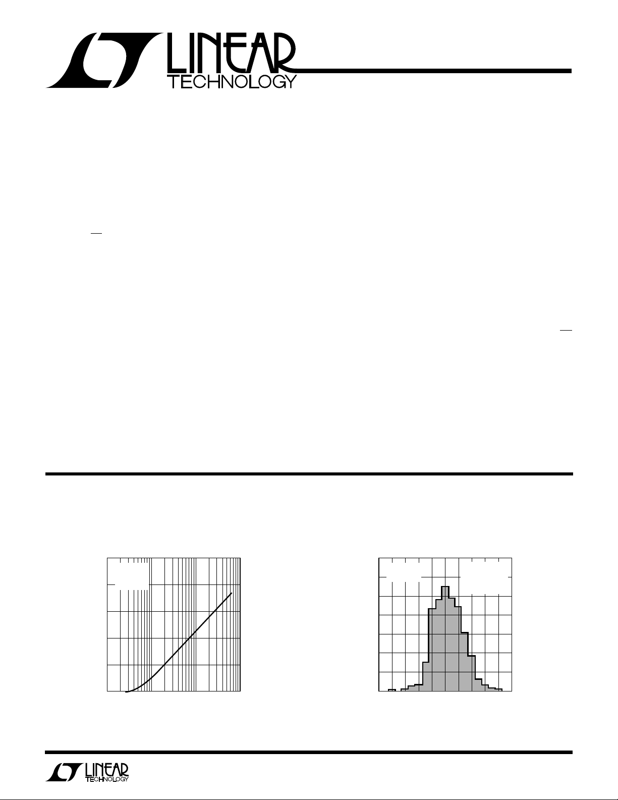
TYPICAL PERFORMANCE CHARACTERISTICS
Capacitive Load Handling
100
VS = ±15V
= 25°C
T
A
= +1
A
80
V
60
40
OVERSHOOT (%)
20
0
0.1 1 10
CAPACITIVE LOAD (nF)
100
LT11457• TA01
PERCENT OF UNITS
Input Offset Voltage Distribution
S8 Package
21
VS = ±15V
T
= 25°C
18
A
15
12
9
6
3
0
–1.0 –0.6 –0.2 0.60.2–0.8 –0.4 0 0.80.4
INPUT OFFSET VOLTAGE (mV)
400 DUALS
(800 OP AMPS)
TESTED FROM
3 RUNS
1.0
LT1457 • TA02
1
LT1457
WW
W
U
ABSOLUTE MAXIMUM RATINGS
Supply Voltage ...................................................... ±20V
Differential Input Voltage .......................................±40V
Input Voltage .......................... Equal to Supply Voltages
Output Short-Circuit Duration.......................... Indefinite
Operating Temperature Range ................ –40°C to 85°C
Storage Temperature Range ................. – 65°C to 150°C
Lead Temperature (Soldering, 10 sec).................. 300°C
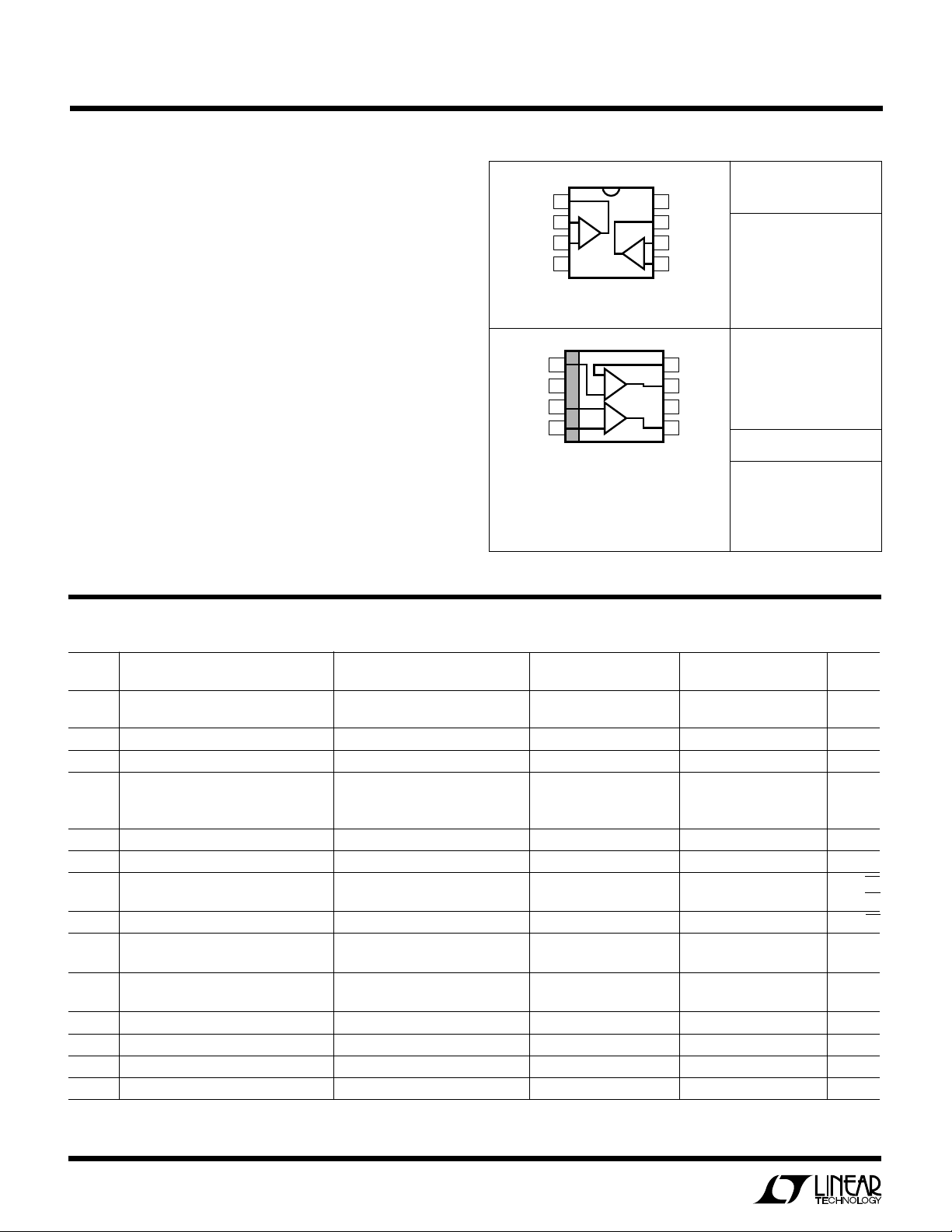
U
W
PACKAGE/ORDER INFORMATION
TOP VIEW
+
1
OUT A
2
–IN A
+IN A
V
+IN A
V
+IN B
–IN B
NOTE: THIS PIN CONFIGURATION DIFFERS FROM
THE 8-LEAD DIP PIN LOCATIONS. INSTEAD, IT
FOLLOWS THE INDUSTRY STANDARD LT1013DS8
SO PACKAGE CONFIGURATION.
Consult factory for Industrial and Military grade parts.
A
3
–
N8 PACKAGE
8-LEAD PLASTIC DIP
T
= 115°C, θJA = 130°C/W
JMAX
TOP VIEW
1
–
2
3
4
S8 PACKAGE
8-LEAD PLASTIC SOIC
T
= 130°C, θJA = 190°C/ W
JMAX
A
B
8
V
7
OUT B
6
–IN B
B
+IN B
54
–IN A
8
7
OUT A
+
6
V
OUT B
5
ORDER PART
NUMBER
LT1457ACN8
LT1457CN8
LT1457S8
S8 PART MARKING
1457
U
ELECTRICAL CHARACTERISTICS
SYMBOL PARAMETER CONDITIONS MIN TYP MAX MIN TYP MAX UNITS
V
OS
I
OS
I
B
e
n
e
n
i
n
A
VOL
CMRR Common-Mode Rejection Ratio VCM = ±10.5V 86 100 82 98 dB
PSRR Power Supply Rejection Ratio VS = ±4.5V to ±18V 88 103 86 102 dB
V
OUT
SR Slew Rate 2 4 2 4 V/µs
Input Offset Voltage LT1457AC/C 150 450 200 800 µV
LT1457S8 220 1200 µV
Input Offset Current Fully Warmed Up 3 40 4 50 pA
Input Bias Current Fully Warmed Up ±5 ±50 ±7 ±75 pA
Input Resistance-Differential 10
-Common-Mode V
Input Capacitance 4 4 pF
Input Noise Voltage 0.1Hz to 10Hz 2.0 2.1 µV
Input Noise Voltage Density fO = 10Hz 26 28 nV/√Hz
Input Noise Current Density fO = 10Hz, 1kHz (Note 3) 1.5 4 1.8 6 fA/√Hz
Large-Signal Voltage Gain VO = ±10V, RL = 2k 150 350 100 300 V/mV
Input Voltage Range ±10.5 14.3 ±10.5 14.3 V
Output Voltage Swing RL = 2k ±12 ±13 ±12 ±13 V
= –11V to 8V 10
CM
VCM = 8V to 11V 10
= 1kHz (Note 2) 13 22 14 24 nV/√Hz
f
O
= ±10V, RL = 1k 120 250 80 220 V/mV
V
O
VS = ±15V, TA = 25°C,VCM = 0V unless otherwise noted. (Note 1)
LT1457AC LT1457C/LT1457S8
12
12
11
–11.5 –11.5 V
10
10
10
12
12
11
P–P
Ω
Ω
Ω
2
LT1457
ELECTRICAL CHARACTERISTICS
SYMBOL PARAMETER CONDITIONS MIN TYP MAX MIN TYP MAX UNITS
GBW Gain-Bandwidth Product (Note 5) 1.0 1.7 1.0 1.7 MHz
I
S
Supply Current Per Amplifier 1.8 3.0 1.8 3.0 mA
Channel Separation DC to 5kHz, VIN = ±10V 132 130 dB
ELECTRICAL CHARACTERISTICS
SYMBOL PARAMETER CONDITIONS MIN TYP MAX MIN TYP MAX UNITS
V
OS
I
OS
I
B
A
VOL
CMRR Common-Mode Rejection Ratio VCM = ±10.4V ● 85 98 80 96 dB
PSRR Power Supply Rejection Ratio VS = ±4.5V to ±18V ● 87 102 84 100 dB
V
OUT
I
S
Input Offset Voltage LT1457AC/C ● 250 900 330 1500 µV
LT1457S8 ● 400 1900 µV
Average Temperature Coefficient of ● 310 416 µV/°C
Input Offset Voltage (Note 4)
Input Offset Current Warmed Up, TA = 70°C 18 150 20 250 pA
Input Bias Current Warmed Up, TA = 70°C ±50 ±250 ±60 ±350 pA
Large-Signal Voltage Gain VO = ±10V, RL = 2k ● 70 220 50 200 V/mV
Output Voltage Swing RL = 2k ● ±12 ±12.8 ±12 ±12.8 V
Supply Current Per Amplifier ● 3.2 3.2 mA
TA = 70°C 1.7 1.7 mA
VS = ±15V, TA = 25°C,VCM = 0V unless otherwise noted. (Note 1)
LT1457AC LT1457C/LT1457S8
VS = ±15V, VCM = 0V, 0°C ≤ TA ≤ 70°C, unless otherwise noted.
LT1457AC LT1457C/LT1457S8
ELECTRICAL CHARACTERISTICS
SYMBOL PARAMETER CONDITIONS MIN TYP MAX MIN TYP MAX UNITS
V
OS
I
OS
I
B
A
VOL
CMRR Common-Mode Rejection Ratio VCM = ±10.4V ● 84 97 80 95 dB
PSRR Power Supply Rejection Ratio VS = ±5V to ±17V ● 86 100 83 98 dB
V
OUT
I
S
The ● denotes the specifications which apply over the full operating
temperature range.
Note 1: Typical parameters are defined as the 60% yield of distributions of
individual amplifiers; i.e., out of 100 LT1457s (200 op amps) typically 120
will be better than the indicated specification.
Note 2: This parameter is tested on a sample basis only.
Note 3: Current noise is calculated from the formula: i
q = 1.6 x 10
swamps the contribution of current noise.
Input Offset Voltage LT1457AC/C ● 350 1100 400 1800 µV
LT1457S8 ● 500 2300 µV
Average Temperature Coefficient of ● 310 416 µV/°C
Input Offset Voltage
Input Offset Current Warmed Up, TA = 85°C 0.1 0.5 0.1 0.6 nA
Input Bias Current Warmed Up, TA = 85°C ±0.2 ±0.7 ±0.2 ±0.9 nA
Large-Signal Voltage Gain VO = ±10V, RL = 2k ● 40 120 30 110 V/mV
Output Voltage Swing RL = 2k ● ±12 ±12.7 ±12 ±12.6 V
Supply Current Per Amplifier TA = – 40°C 3.8 3.8 mA
TA = 85°C 1.7 1.7 mA
= (2qIb)
–19
coulomb. The noise of source resistors up to 1GΩ
n
VS = ±15V, VCM = 0V, –40°C ≤ TA ≤ 85°C, unless otherwise noted. (Note 6)
LT1457AC LT1457C/LT1457S8
Note 4: This parameter is not 100% tested.
Note 5: Gain-Bandwidth product is not tested. It is guaranteed by design
and by inference from the slew rate measurement.
Note 6: The LT1457 is not tested and not quality-assurance-sampled at
–40°C and at 85°C. These specifications are guaranteed by design,
correlation, and/or inference from 0°C, 25°C, and 70°C tests.
1/2
, where
3
 Loading...