

Linear Technology LT1432-3.3 Datasheet
LT1432-3.3
3.3V High Efficiency Step-Down
Switching Regulator Controller
EATU
F
■
Accurate Preset 3.3V Output
■
Up to 87% Efficiency
■
Optional Burst ModeTM Operation for Light Loads
■
Can Be Used with Many LTC Switching ICs
■
Accurate Ultra-Low-Loss Current Limit
■
Operates with Inputs from 4.5V to 30V
■
Shutdown Mode Draws Only 15µA
■
Uses Small 30µH Inductor
PPLICATI
A
■
Laptop and Palmtop Computers
■
Portable Data-Gathering Instruments
, LTC and LT are registered trademarks of Linear Technology Corporation.
Burst Mode is a trademark of Linear Technology Corporation.
RE
S
O
U
S
DUESCRIPTIO
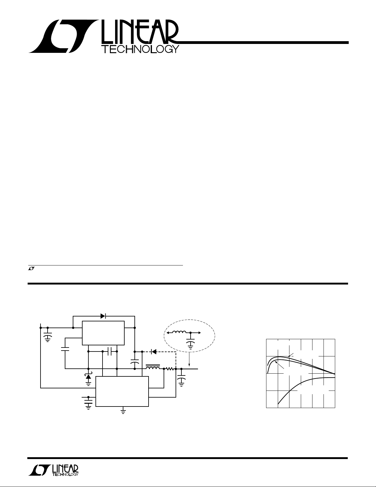
The LT®1432-3.3 is a control chip designed to operate
with the LT1171/LT1271 family of switching regulators to
make a very high efficiency 3.3V step-down (buck) switching regulator. A minimum of external components is
needed.
Included is an accurate current limit which uses only
60mV sense voltage and uses “free” PC board trace
material for the sense resistor. Logic controlled electronic
shutdown mode draws only 15µA battery current. The
switching regulator operates down to 4.5V input.
The LT1432-3.3 has a logic controlled Burst Mode operation
to achieve high efficiency at very light load currents (0mA to
100mA) such as memory keep-alive. In normal switching
mode, the standby power loss is about 30mW, limiting
efficiency at light loads. In Burst Mode operation, standby
loss is reduced to approximately 11mW. Output current in
this mode is typically in the 5mA to 100mA range.
The LT1432-3.3 is available in 8-pin SO and PDIP packages. The LT1171/LT1271 is also available in surface
mount DD packages.
V
IN
+
C1
330µF
35V
MODE LOGIC
<0.3V = NORMAL MODE
>2.5V = SHUTDOWN
OPEN = Burst Mode
OPERATION
U
O
A
PPLICATITYPICAL
D2
1N5818
V
SW
LT1271
FB
V
C
C6
0.02µF
D1
MBR330p
V
MODE
220pF
†
FOR CIRCUITS WHICH DO NOT USE
Burst Mode OPERATION, C5 MAY
BE PARALLEL WITH A 680Ω, 0.1µF
IN SERIES TO GIVE WIDE PHASE MARGIN
WITH DIFFERENT SWITCHING ICs AND
OUTPUT CAPACITORS
V
IN
GND
C3
10µF
TANT
DIODE
LT1432-3.3
GND
+
†
C5
0.03µF
V
C
IN
D2**
L1
R2*
30µH
0.013Ω
+
V
V
LIM
V
OUT
*R2 IS MADE FROM PC BOARD
COPPER TRACES.
**OPTIONAL CONNECTION FOR D2.
EFFICIENCY IS HIGHER, BUT MINIMUM
INCREASES. SEE APPLICATION
V
IN
INFORMATION SECTION.
***MAXIMUM CURRENT IS DETERMINED
BY THE CHOICE OF LT1071 FAMILY MAIN SWITCHER IC.
SEE APPLICATION INFORMATION SECTION.
Figure 1. High Efficiency 5V Buck Converter
10µH
3A
100µF
16V
+
+
×
C2
390µF
16V
OPTIONAL
OUTPUT
FILTER
***
V
OUT
3.3V
3A
LT1432-3.3 TA01
100
LT1271, L = 30µH
VIN = 7V
90
80
EFFICIENCY (%)
70
60
0
0
Efficiency
D2 CONNECTED
TO OUTPUT
D2 CONNECTED
TO INPUT
Burst Mode OPERATION
(USE mA SCALE)
1A 2A
20mA
40mA
60mA
LT1432-3.3 TA02
3A
1
LT1432-3.3
WU
U
PACKAGE
/
O
RDER I FOR ATIO
1
2
3
4
TOP VIEW
V
LIM
V
OUT
V
IN
V
+
MODE
GND
V
C
DIODE
N8 PACKAGE
8-LEAD PDIP
8
7
6
5
S8 PACKAGE
8-LEAD PLASTIC SO
W
O
A
LUTEXI T
S
VIN Pin .................................................................... 30V
V+ Pin ..................................................................... 40V
A
WUW
ARB
U
G
I
S
ORDER PART
NUMBER
VC........................................................................... 35V
V
and V
LIM
Diode Pin Voltage ................................................... 30V
Pins................................................... 7V
OUT
LT1432CN8-3.3
LT1432CS8-3.3
Mode Pin Current (Note 2) ..................................... 1mA
Operating Temperature Range .................... 0°C to 70°C
Storage Temperature Range ................ –65°C to 150°C
Lead Temperature (Soldering, 10 sec)................. 300°C
LECTRICAL C CHARA TERIST
E
VC = 4V, VIN = 4V, V+ = 8V, V
Device is in standard test loop unless otherwise noted.
PARAMETER CONDITIONS MIN TYP MAX UNITS
Regulated Output Voltage VC Current = 220µA ● 3.24 3.30 3.36 V
Output Voltage Line Regulation VIN = 4V to 30V ● 520mV
Input Supply Current (Note 1) VIN = 4V to 30V, V+ = VIN + 5V, VC = VIN + 1V ● 0.3 0.5 mA
Quiescent Output Load Current 0.9 1.2 mA
Mode Pin Current V
Mode Pin Threshold Voltage I
(Normal to Burst)
VC Pin Saturation Voltage V
VC Pin Maximum Sink Current V
VC Pin Source Current V
Current Limit Sense Voltage (Note 3) Device in Current Limit Loop 56 60 64 mV
Pin Current Device in Current Limit Loop ● 30 45 70 µA
V
LIM
Supply Current in Shutdown V
Burst Mode Operation Output Ripple Device in Burst Test Circuit 100 mV
Burst Mode Operation Average Output Voltage Device in Burst Test Circuit ● 3.15 3.30 3.45 V
Clamp Diode Forward Voltage IF = 1mA, All Other Pins Open ● 0.5 0.65 V
Start-up Drive Current V
Restart Time Delay (Note 4) 0.7 1.2 10 ms
Transconductance, Output to VC Pin IC = 150µA to 250µA ● 2700 3600 5000 µmho
DIODE
= Open, V
ICS
= V
LIM
MODE
V
MODE
MODE
OUT
OUT
OUT
(Current Is Out of Pin)
MODE
OUT
V+ = VIN – 1V, VC = V
, V
OUT
= 0V (Current Is Out of Pin) ● 30 50 µA
= 3.3V (Shutdown) ● 15 30 µA
= 10µA (Out of Pin) ● 0.6 0.9 1.5 V
= 3.6V (Forced) ● 0.25 0.45 V
= 3.6V (Forced) ● 0.45 0.8 1.5 mA
= 3.0V (Forced) ● 35 60 100 µA
> 3V, VIN < 30V, VC and V+ = 0V 15 60 µA
= 1.5V (Forced), VIN = 4V to 26V, ● 30 45 mA
= 0V, TJ = 25°C
MODE
– 1.5V
IN
T
= 100°C, θJA = 150°C/W (N8)
JMAX
T
= 100°C, θJA = 170°C/W (S8)
JMAX
Consult factory for Military and Industrial grade parts.
p-p
2
LT1432-3.3
LECTRICAL C CHARA TERIST
E
Operating parameters in standard circuit configuration.
VIN = 7V, I
PARAMETER CONDITIONS MIN TYP MAX UNITS
Burst Mode Operation Quiescent Input Supply Current 1.6 2.2 mA
Burst Mode Operation Output Ripple Voltage I
Normal Mode Equivalent Input Supply Current Extrapolated from I
Normal Mode Minimum Operating Input Voltage 100mA < I
Burst Mode Operation Minimum Operating Input Voltage 5mA < I
Efficiency Normal Mode I
Load Regulation Normal Mode 50mA < I
= 0, unless otherwise noted. These parameters guaranteed where indicated, but not tested.
OUT
ICS
= 0 80 mV
OUT
I
= 50mA 120 mV
OUT
= 20mA 3.0 mA
OUT
< 1.5A 4.5 V
OUT
< 50mA 4.1 V
OUT
= 0.5A 86 %
Burst Mode Operation I
Burst Mode Operation 0 < I
OUT
= 25mA 70 %
OUT
< 2A 5 15 mV
OUT
< 50mA 30 mV
OUT
p-p
p-p
The ● denotes specifications which apply over the full operating
temperature range.
Note 1: Does not include current drawn by the power IC. See operating
parameters in standard circuit.
Note 2: Breakdown voltage on the Mode pin is 7V. External current must
be limited to value shown.
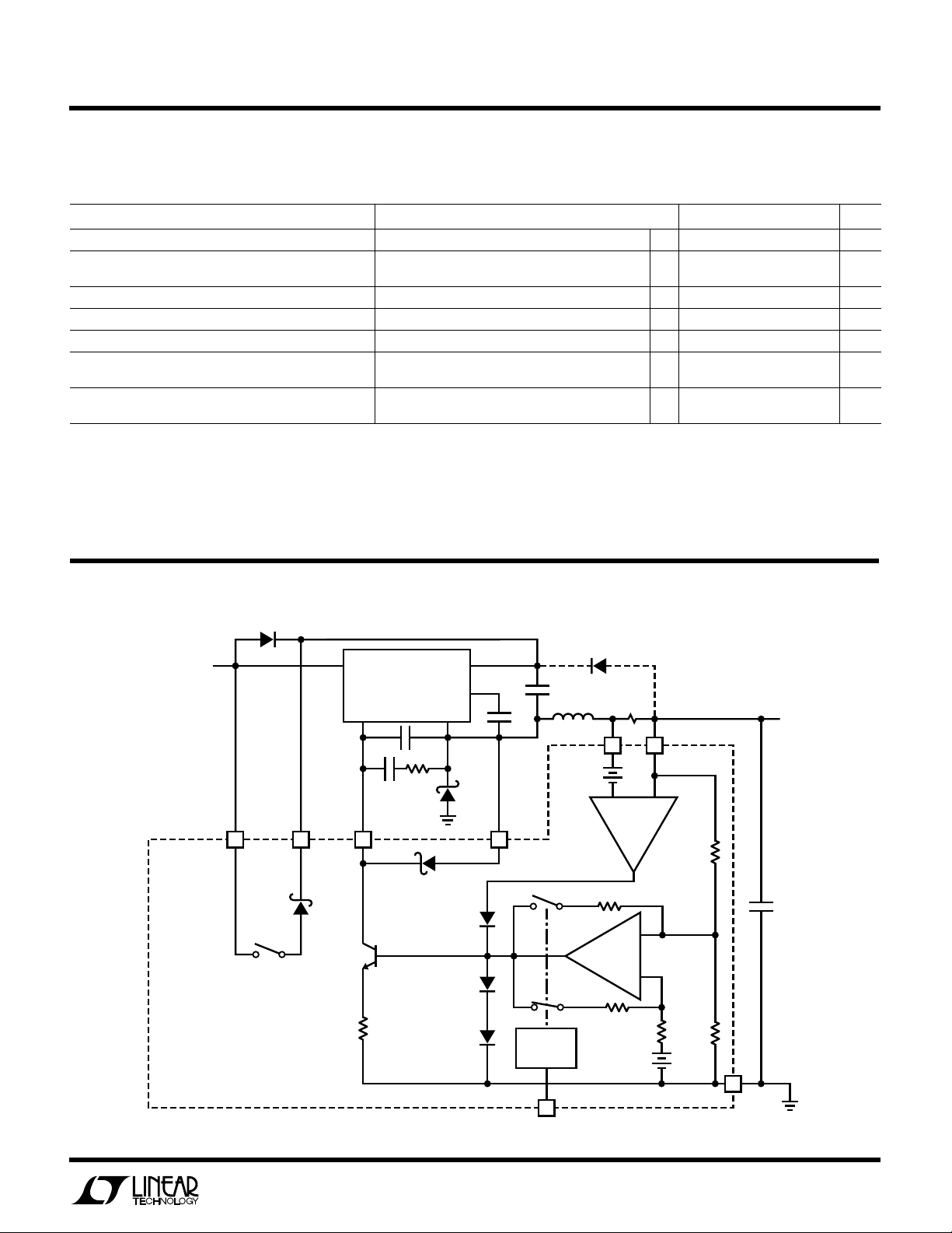
U
T
S
CH
V
IN
V
IN
34
W
A
E
D2
V
CEQUIVALE
TI
V
SW
LT1271
V
C
+
V
C
65
V
GND
Note 3: Current limit sense voltage temperature coefficient is +0.33%/°C
to match TC of copper trace material.
Note 4: V
IN
FB
DIODE
pin switched from 3.6V to 3.0V.
OUT
OPTIONAL
CONNECTION
OF D2
V
OUT
2
–
S1**
V
60mV
LIM
1
+
3.3V
S3*
* S3 IS CLOSED ONLY DURING START-UP.
** S1 AND S2 ARE SHOWN IN NORMAL
MODE. REVERSE FOR Burst Mode
OPERATION.
Figure 2
S2**
MODE
CONTROL
MODE
8
+
–
7
GND
LT1432-3.3 F02
3
 Loading...