

Linear Technology LT1432 Datasheet
LT1432
0
60
EFFICIENCY (%)
70
80
90
100
1A 2A
3A
20mA
LT1432 TA02
40mA
60mA
0
NORMAL MODE
(USE AMPS SCALE)
BURST MODE
(USE mA SCALE)
LT1271, L = 50µH
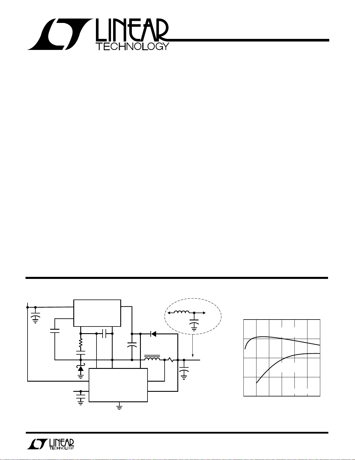
5V High Efficiency Step-Down
Switching Regulator Controller
EATU
F
■
Accurate Preset +5V Output
■
Up to 90% Efficiency
■
Optional Burst Mode for Light Loads
■
Can be Used with Many LTC Switching ICs
■
Accurate Ultra-Low-Loss Current Limit
■
Operates with Inputs from 6V to 30V
■
Shutdown Mode Draws Only 15µA
■
Uses Small 50µH Inductor
PPLICATI
A
■
Laptop and Palmtop Computers
■
Portable Data-Gathering Instruments
■
DC Bus Distribution Systems
■
Battery-Powered Digital Widgets
RE
S
O
U
S
DUESCRIPTIO
The LT1432 is a control chip designed to operate with the
LT1170/LT1270 family of switching regulators to make a
very high efficiency 5V step-down (buck) switching regulator. A minimum of external components is needed.
Included is an accurate current limit which uses only 60mV
sense voltage and uses “free” PC board trace material for
the sense resistor. Logic controlled electronic shutdown
mode draws only 15µA battery current. The switching
regulator operates down to 6V input.
The LT1432 has a logic controlled “burst” mode to achieve
high efficiency at very light load currents (0 to 100mA) such
as memory keep-alive. In normal switching mode, the
standby power loss is about 60mW, limiting efficiency at
light loads. In burst mode, standby loss is reduced to
approximately 15mW. Output current in this mode is
typically in the 5mA to 100mA range.
The LT1432 is available in 8-pin surface mount and DIP
packages. The LT1170/LT1270 family will also be available
in a surface mount version of the 5-pin TO-220 package.
For 3.3V versions contact Linear Technology Corporation.
V
IN
+
C1
330µF
35V
C6
0.02µF
MBR330p
MODE LOGIC
<0.3V = NORMAL MODE
>2.5V = SHUTDOWN
OPEN = BURST MODE
U
O
A
PPLICATITYPICAL
0.1µF
220pF
V
SW
LT1170
LT1271
FB
V
C
R1
680Ω
C4
D1
V
V
IN
MODE
0.03µF
C
C5
V
GND
DIODE
LT1432
IN
4.7µF
TANT
GND
D2
1N4148
C3
+
L1
50µH
+
V
V
LIM
V
OUT
* R2 IS MADE FROM PC BOARD
COPPER TRACES.
** MAXIMUM CURRENT IS DETERMINED
BY THE CHOICE OF LT1070 FAMILY.
SEE APPLICATION SECTION.
Figure 1. High Efficiency 5V Buck Converter
R2*
0.013Ω
10µH
3A
100µF
16V
+
+
×
C2
390µF
16V
OPTIONAL
OUTPUT
FILTER
V
OUT
5V
3A**
LT1432 TA01
Efficiency
1

LT1432
WU
U
PACKAGE
/
O
RDER I FOR ATIO
W
O
A
LUTEXI T
S
VIN Pin .................................................................... 30V
V+ Pin ..................................................................... 40V
VC........................................................................... 35V
V
LIM
and V
Pins................................................... 7V
OUT
Diode Pin Voltage ................................................... 30V
Mode Pin Current (Note 2) ..................................... 1mA
Operating Temperature Range .................... 0°C to 70°C
Storage Temperature Range ................ –65°C to 150°C
Lead Temperature (Soldering, 10 sec.)................ 300°C
LECTRICAL C CHARA TERIST
E
VC = 6V, VIN = 12V, V+ = 10V, V
Device is in standard test loop unless otherwise noted.
PARAMETER CONDITIONS MIN TYP MAX UNITS
Regulated Output Voltage VC Current = 220µA ● 4.9 5.0 5.1 V
Output Voltage Line Regulation VIN = 6V to 30V ● 520 mV
Input Supply Current (Note 1) VIN = 6V to 30V, V+ = VIN + 5V, VC = VIN + 1V ● 0.3 0.5 mA
Quiescent Output Load Current 0.9 1.2 mA
Mode Pin Current V
Mode Pin Threshold Voltage I
(Normal to Burst)
VC Pin Saturation Voltage V
VC Pin Maximum Sink Current V
VC Pin Source Current V
Current Limit Sense Voltage (Note 3) Device in Current Limit Loop 56 60 64 mV
Pin Current Device in Current Limit Loop ● 30 45 70 µA
V
LIM
Supply Current in Shutdown V
Burst Mode Output Ripple Device in Burst Test Circuit 100 mV
Burst Mode Average Output Voltage Device in Burst Test Circuit ● 4.8 5 5.2 V
Clamp Diode Forward Voltage IF = 1mA, All Other Pins Open ● 0.5 0.65 V
Startup Drive Current V
Restart Time Delay (Note 4) 1 1.8 10 ms
Transconductance, Output to VC Pin IC = 150µA to 250µA ● 1500 2000 2800 µmho
The ● denotes specifications which apply over the operating temperature
range.
Note 1: Does not include current drawn by the LT1070 IC. See operating
parameters in standard circuit.
Note 2: Breakdown voltage on the mode pin is 7V. External current must
be limited to value shown.
A
WUW
= Open, V
DIODE
U
ARB
G
I
S
1
V
LIM
2
V
OUT
3
V
IN
+
4
V
8-LEAD PLASTIC DIP
8-LEAD PLASTIC SO
TOP VIEW
N8 PACKAGE
S8 PACKAGE
ORDER PART
MODE
8
GND
7
V
6
C
DIODE
5
NUMBER
LT1432CN8
LT1432CS8
ICS
= V
, V
LIM
OUT
= 0V (current is out of pin) ● 30 50 µA
MODE
V
= 5V (shutdown) ● 15 30 µA
MODE
= 10µA (out of pin) ● 0.6 0.9 1.5 V
MODE
= 5.5V (forced) ● 0.25 0.45 V
OUT
= 5.5V (forced) ● 0.45 0.8 1.5 mA
OUT
= 4.5V (forced) ● 40 60 100 µA
OUT
(current is out of pin)
> 3V, VIN < 30V, VC and V+ = 0V ● 15 60 µA
MODE
= 2.5V (forced), V+ = 5V to 25V, ● 30 45 mA
OUT
VIN = 6V to 26V, V+ = VIN – 1V, VC = V
= 0V, TJ = 25°C
MODE
– 1.5V
IN
Note 3: Current limit sense voltage temperature coefficient is +0.33%/°C
to match TC of copper trace material.
Note 4: V
pin switched from 5.5Vto 4.5V.
OUT
p-p
2
LT1432
LECTRICAL C CHARA TERIST
E
Operating parameters in standard circuit configuration.
VIN = +12V, I
PARAMETER CONDITIONS MIN TYP MAX UNITS
Burst Mode Quiescent Input Supply Current 1.3 1.8 mA
Burst Mode Output Ripple Voltage I
Normal Mode Equivalent Input Supply Current Extrapolated from I
Normal Mode Minimum Operating Input Voltage 100mA < I
Burst Mode Minimum Operating Input Voltage 5mA < I
Efficiency Normal Mode I
Load Regulation Normal Mode 50mA < I
= 0, unless otherwise noted. These parameters guaranteed where indicated, but not tested.
OUT
ICS
= 0 100 mV
OUT
I
= 50mA 130 mV
OUT
= 20mA 6 mA
OUT
< 1.5A 6 V
OUT
< 50mA 6.2 V
OUT
= 0.5A 91 %
Burst Mode I
Burst Mode 0 < I
OUT
= 25mA 77 %
OUT
< 2A 10 25 mV
OUT
< 50mA 50 mV
OUT
p-p
p-p
U
T
V
IN
E
S
CH
V
IN
34
S3*
W
A
V
CEQUIVALE
TI
V
SW
LT1271
V
C
+
V
C
65
GND
V
IN
FB
DIODE
S1**
V
60mV
LIM
+5V
V
1
+
OUT
2
–
+
* S3 IS CLOSED ONLY DURING STARTUP.
** S1 AND S2 ARE SHOWN IN NORMAL
MODE. REVERSE FOR BURST MODE.
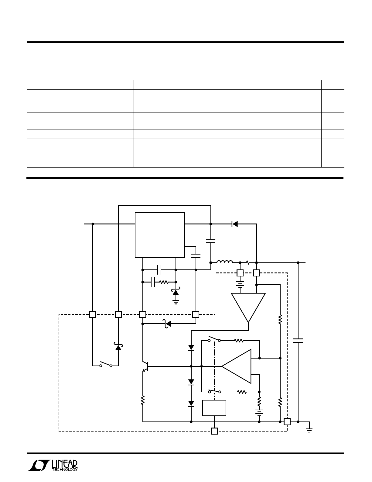
Figure 2
S2**
MODE
CONTROL
MODE
8
–
7
GND
LT1432 F02
3
LT1432
JUNCTION TEMPERATURE (°C)
0
SENSE VOLTAGE (mV)
60
70
100
LT1432 G11
50
40
25
50
75
80
* TEMPERATURE COEFFICIENT OF SENSE VOLTAGE IS
DESIGNED TO TRACK COPPER RESISTANCE.
OUTPUT CURRENT (A)
0
INPUT VOLTAGE (V)
6.5
7.0
7.5
4
LT1432 G03
6.0
5.5
5.0
1
2
3
5
LT1270
LT1271
LT1270/1271
T
J
= 25°C
LPER
Efficiency vs Input Voltage
100
90
I
80
LOAD
I
LOAD
I
LOAD
F
= 2A
O
= 0.5A
= 1A
R
ATYPICA
UW
CCHARA TERIST
E
C
Efficiency vs Load Current
100
L = 50µH
90
LT1170
80
L = 25µH
LT1271
ICS
LT1270
L = 50µH
Minimum Input Voltage – Normal
Mode (1270/1271)
EFFICIENCY (%)
70
TJ = 25°C
LT1271, L = 50µH
60
0
5101520
INPUT VOLTAGE (V)
Minimum Input Voltage – Normal
Mode (1070 Family)
7.5
LT1070 FAMILY(40kHz)
= 25°C
T
J
7.0
6.5
6.0
INPUT VOLTAGE (V)
5.5
5.0
0
LT1072
LT1071
1
2
OUTPUT CURRENT (A)
LT1070
3
25 30
LT1432 G01
4
LT1432 G04
EFFICIENCY (%)
70
TJ = 25°C
60
0
0.5 1.0 1.5 2.0
LOAD CURRENT (A)
Minimum Input Voltage – Normal
Mode (1170 Family)
7.5
LT1170 FAMILY(100kHz)
= 25°C
T
J
7.0
LT1172
6.5
6.0
INPUT VOLTAGE (V)
5.5
5
5.0
0
LT1171
1
2
OUTPUT CURRENT (A)
2.5 3.0
LT1432 G02
Burst Mode Minimum Input
Voltage
7.0
TJ = 25°C
LT1170
3
4
5
LT1432 G05
6.5
LT1170
6.0
INPUT VOLTAGE (V)
5.5
5.0
10
0
LT1070
30
20
LOAD CURRENT (mA)
40
50
LT1432 G06
Shutdown Current vs Input
Voltage
50
TJ = 25°C
40
30
20
CURRENT (µA)
10
0
0
5
4
10 15 20
INPUT VOLTAGE (V)
25 30
LT1432 G07
Battery Current in Shutdown*
40
30
20
CURRENT (µA)
10
0
0
*DOES NOT INCLUDE LT1271 SWITCH LEAKAGE.
V
= 30V
IN
VIN = 6V
25
50
TEMPERATURE (°C)
75
Current Limit Sense Voltage*
100
LT1432 G08
LPER
MODE PIN VOLTAGE (V)
0
CURRENT (µA)
20
40
60
8
LT1432 G15
0
–20
–40
2
4
6
10
MODE DRIVE MUST
SINK ≈ 30µA AT 0V
TJ = 25°C
V+ TO VIN VOLTAGE
–2
V+ PIN CURRENT (mA)
–20
0
5
20
LT1432 G18
–40
–60
–80
–1
0
10
30
TJ = 25°C
NOTE VERTICAL &
HORIZONTAL SCALE
CHANGES AT 0,0
F
O
R
ATYPICA
UW
CCHARA TERIST
E
C
LT1432
ICS
Incremental Battery Current * in
Burst Mode
2.0
TJ = 25°C
1.5
1.0
0.5
INCREMENTAL FACTOR (mA/mA)
0
* TO CALCULATE TOTAL BATTERY CURRENT IN BURST
MODE, MULTIPLY LOAD CURRENT BY INCREMENTAL
FACTOR AND ADD NO-LOAD CURRENT.
5
0
BATTERY VOLTAGE (V)
15
20
10
25
LT1432 G10
Line Regulation
40
TJ = 25°C
BURST MODE
20
No Load Battery Current in Burst
Mode
5
TJ = 25°C
4
3
2
BATTERY CURRENT (mA)
1
0
5
0
BATTERY VOLTAGE (V)
15
10
Burst Mode Load Regulation
25
TJ = 25°C
0
20
LT1432 G09
Transconductance – V
OUT
to V
C
Current
4000
3000
2000
1000
TRANSCONDUCTANCE (µmho)
25
40
∆I(V
PIN)
C
Gm =
∆V
OUT
0
25
JUNCTION TEMPERATURE (°C)
50
75
100
LT1432 G12
Mode Pin Current
0
OUTPUT CHANGE (mV)
–20
–40
40
30
20
CURRENT (mA)
10
0
NORMAL MODE
0
5
10
INPUT VOLTAGE (V)
Restart Load Current
V
= 4.5V
OUT
0
25
JUNCTION TEMPERATURE (°C)
50
–25
OUTPUT CHANGE (mV)
–50
15
75
20
LT1432 G13
100
LT1432 G16
–75
20
0
Restart Time Delay
4
3
2
TIME DELAY (ms)
1
0
0
25
JUNCTION TEMPERATURE (°C)
60
40
LOAD CURRENT (mA)
50
80
100
LT1432 G14
Startup Switch Characteristics
75
100
LT1432 G16
5

LT1432
U
O
PPLICATI
A
Basic Circuit Description
The LT1432 is a dedicated 5V buck converter driver chip
intended to be used with an IC switcher from the LT1070
family. This family of current mode switchers includes
current ratings from 1.25A to 10A, and switching frequencies from 40kHz to 100kHz as shown in the table below.
SWITCH OUTPUT CURRENT IN
DEVICE CURRENT FREQUENCY BUCK CONVERTER
LT1270A 10A 60kHz 7.5A
LT1270 8A 60kHz 6A
LT1170 5A 100kHz 3.75A
LT1070 5A 40kHz 3.75A
LT1271 4A 60kHz 3A
LT1171 2.5A 100kHz 1.8A
LT1071 2.5A 40kHz 1.8A
LT1172 1.25A 100kHz 0.9A
LT1072 1.25A 40kHz 0.9A
The maximum load current which can be delivered by
these chips in a buck converter is approximately 75% of
their switch current rating. This is partly due to the fact that
buck converters must operate at very high duty cycles
when input voltage is low. The “current mode” nature of
the LT1070 family requires an internal reduction of peak
current limit at high duty cycles, so these devices are rated
at only 80% of their full current rating when duty cycle is
80%. A second factor is inductor ripple current, half of
which subtracts from maximum available load current.
See Inductor Selection for details. The LT1070 family was
originally intended for topologies which have the negative
side of the switch grounded, such as boost converters. It
has an extremely efficient quasi-saturating NPN switch
which mimics the linear resistive nature of a MOSFET but
consumes much less die area. Driver losses are kept to a
minimum with a patented adaptive antisat drive that maintains a forced beta of 40 over a wide range of switch
currents. This family is attractive for high efficiency buck
converters because of the low switch loss, but to operate
as a positive buck converter, the ground pin of the IC must
be floated to act as the switch output node. This requires
a floating power supply for the chip and some means for
level shifting the feedback signal. The LT1432 performs
these functions as well as adding current limiting, micropower shutdown, and dual mode operation for high
conversion efficiency with both heavy and very light loads.
S
I FOR ATIO
WU
U
The circuit in Figure 1 is a basic 5V positive buck converter
which can operate with input voltage from 6V to 30V. The
power switch is located between the VSW pin and GND pin
on the LT1271. Its current and duty cycle are controlled by
the voltage on the VC pin with respect to the GND pin. This
voltage ranges from 1V to 2V as switch current increases
from zero to full scale. Correct output voltage is maintained by the LT1432 which has an internal reference and
error amplifier (see Equivalent Schematic in Figure 2). The
amplifier output is level shifted with an internal open
collector NPN to drive the VC pin of the switcher. The
normal resistor divider feedback to the switcher feedback
pin cannot be used because the feedback pin is referenced
to the GND pin, which is switching up and down. The
feedback pin (FB) is simply bypassed with a capacitor.
This forces the switcher VC pin to swing high with about
200µA sourcing capability. The LT1432 VC pin then sinks
this current to control the loop. Transconductance from
the regulator output to the VC pin current is controlled to
approximately 2000µmhos by local feedback around the
LT1432 error amplifier (S2 closed in Figure 2). This is done
to simplify frequency compensation of the overall loop. A
word of caution about the FB pin bypass capacitor (C6):
this capacitor value is very non-critical, but the capacitor
must be connected directly to the GND pin or tab of the
switcher to avoid differential spikes created by fast switch
currents flowing in the external PCB traces. This is also
true for the frequency compensation capacitors C4 and
C5. C4 forms the dominant loop pole with a loop zero
added by R1. C5 forms a higher frequency loop pole to
control switching ripple at the VC pin.
A floating 5V power supply for the switcher is generated by
D2 and C3 which peak detect the output voltage during
switch “off” time. The diode used for D2 is a low capacitance type to avoid spikes at the output. Do not substitute
a Schottky diode for D2 (they are high capacitance). This
is a very efficient way of powering the switcher because
power drain does not increase with regulator input voltage. However, the circuit is not self-starting, so some
means must be used to start the regulator. This is performed by the internal current path of the LT1432 which
allows current to flow from the input supply to the V+ pin
during startup.
6

LT1432
P
VV V I
V
FIN–OUT OUT
IN
=
()()
U
O
PPLICATI
A
D1, L1 and C2 act as the conventional catch diode and
output filter of the buck converter. These components
should be selected carefully to maintain high efficiency
and acceptable output ripple. See other sections of this
data sheet for detailed discussions of these parts.
Current limiting is performed by R2. Sense voltage is only
60mV to maintain high efficiency. This also reduces the
value of the sense resistor enough to utilize a printed
circuit board trace as the sense resistor. The sense voltage
has a positive temperature coefficient of 0.33%/°C to
match the temperature coefficient of copper. See Current
Limiting section for details.
The basic regulator has three different operating modes,
defined by the mode pin drive. Normal operation occurs
when the mode pin is grounded. A low quiescent current
“burst” mode can be initiated by floating the mode pin.
Input supply current is typically 1.3mA in this mode, and
output ripple voltage is 100mV
above 2.5V forces the entire regulator into micropower
shutdown where it typically draws less than 20µA. See
Mode Pin Drive for details.
Efficiency
Efficiency in normal mode is maximum at about 500mA
load current, where it exceeds 90%. At lower currents, the
operating supply current of the switching IC dominates
losses. The power loss due to this term is approximately
8mA × 5V, or 40mW. This is 4% of output power at a load
current of 200mA. At higher load currents, losses in the
switch, diode, and inductor series resistance begin to
increase as the square of current and quickly become the
dominant loss terms.
Loss in inductor series resistance;
P = RS (I
Loss in switch on resistance;
VRI
P
=
Loss in switch driver current;
)
OUT
()
OUT SW
S
I FOR ATIO
2
2
()
OUT
V
IN
p-p
WU
. Pulling the mode pin
U
IV
()
OUT OUT
P
=
40V
Diode loss;
(Use
VF vs I
I
)
OUT
RS = Inductor series resistance
RSW = Switch resistance of LT1271, etc.
IF = Diode current
VF = Diode forward voltage at IF = I
Inductor core loss depends on peak-to-peak ripple current
in the inductor, which is independent of load current for
any load current large enough to establish continuous
current in the inductor. Believe it or not, core loss is also
independent of the physical size of the core. It depends
only on core material, inductance value, and switching
frequency for fixed regulator operating conditions. Increasing inductance or switching frequency will reduce
core loss, because of the resultant decrease in ripple
current. For high efficiency, low loss cores such as ferrites
or Magnetics Inc. molypermalloy or KoolMµ are recommended. The lower cost Type 52 powdered iron from
Phillips is acceptable only if larger inductance is used and
the increased size and slight loss in efficiency is acceptable. In a typical buck converter using the LT1271 (60kHz)
with a 12V input, and a 50µH inductor, core loss with a
Type 52 powdered iron core is 203mW. A molypermalloy
core reduces this figure to 28mW. With a 1A output, this
translates to 4% and 0.56% core loss respectively – a big
difference in a high efficiency converter. For details on
inductor design and losses, see Application Note 44.
What are the benefits of using an active (synchronous)
switch to replace the catch diode? This is the trendy thing
to do, but calculations and actual breadboards show that
the improvement in efficiency is only a few percent at best.
This can be shown with the following simplified formulas:
Diode Loss
F
2
IN
graph on diode data sheet, assuming IF =
OUT
VV V I
()()
FIN–OUT OUT
=
V
IN
7

LT1432
U
O
PPLICATI
A
FET Switch Loss
(Ignoring gate drive power)
The change in efficiency is:
Diode Loss – FET Loss Efficiency
()()
This is equal to:
V–V V–R I E
()
IN OUT F FET OUT
If VF (diode forward voltage) = 0.45V, VIN = 10V, V
R
= 0.1Ω, I
FET
ment in efficiency is only:
10V – 5V 0.45V – 0.1 1A 0.9
()
This does not take FET gate drive losses into account,
which can easily reduce this figure to less than 2%. The
added cost, size, and complexity of a synchronous switch
configuration would be warranted only in the most extreme circumstances.
Burst mode efficiency is limited by quiescent current drain
in the LT1432 and the switching IC. The typical burst mode
zero-load input power is 27mW. This gives about one
month battery life for a 12V, 1.2AHr battery pack. Increasing load power reduces discharge time proportionately.
Full shutdown current is only about 15µA, which is considerably less than the self-discharge rate of typical batteries.
Burst Mode Operation
Burst mode is initiated by allowing the mode pin to float,
where it will assume a DC voltage of approximately 1V. If
AC pickup from surrounding logic lines is likely, the mode
pin should be bypassed with a 200pF capacitor. Burst
mode is used to reduce quiescent operating current when
the regulator output current is very low, as in “sleep” mode
OUT
()()
S
I FOR ATIO
VV R I
()()()
IN–OUT SW OUT
=
VV
()( )
IN OUT
×
()()
VV
()( )
IN OUT
= 1A, and efficiency = 90%, the improve-
10V 5V
()()
×
Ω
WU
V
IN
2
2
OUT
2
2.8%
=
U
2
= 5V,
in a lap-top computer. In this mode, hysteresis is added to
the error amplifier to make it switch on and off, rather than
maintain a constant amplifier output. This forces the
switching IC to either provide a rapidly increasing current
or to go into full micropower shutdown. Current is delivered to the output capacitor in pulses of higher amplitude
and low duty cycle rather than a continuous stream of low
amplitude pulses. This maximizes efficiency at light load
by eliminating quiescent current in the switching IC during
the period between bursts.
The result of pulsating currents into the output capacitor
is that output ripple amplitude increases, and ripple frequency becomes a function of load current. The typical
output ripple in burst mode is 150mVp-p, and ripple
frequency can vary from 50Hz to 2kHz. This is not normally
a problem for the logic circuits which are kept “alive”
during sleep mode.
Some thought must be given to proper sequencing between normal mode and burst mode. A heavy (>100mA)
load in burst mode can cause excessive output ripple, and
an abnormally light load (10mA to 30mA, see curves) in
normal mode can cause the regulator to revert to a quasiburst mode that also has higher output ripple. The worst
condition is a sudden, large increase in load current
(>100mA) during this quasi-burst mode or just after a
switch from burst mode to normal mode. This can cause
the output to sag badly while the regulator is establishing
normal mode operation (≈100µs). To avoid problems, it is
suggested that the power-down sequence consist of reducing load current to below 100mA, but greater than the
minimum for normal mode, then switching to burst mode,
followed by a reduction of load current to the final sleep
value. Power-up would consist of increasing the load
current to the minimum for normal mode, then switching
to normal mode, pausing for 1ms, followed by return to
full load.
If this sequence is not possible, an alternative is to
minimize normal mode settling time by adding a 47kΩ
resistor between V+ and VC pins. The output capacitor
should be increased to >680µF and the compensation
capacitors should also be as small as possible, consistent
with adequate phase margin. These modifications will
8
LT1432
PPLICATI
A
U
O
S
I FOR ATIO
WU
U
often allow the power-down sequence to consist of simultaneous turn-off of load current and switch to burst mode.
Power-up is accomplished by switching to normal mode
and simultaneously increasing load current to the lowest
possible value (30mA to 500mA), followed by a short
pause and return to full load current.
Full Shutdown
When the mode pin is driven high, full shutdown of the
regulator occurs. Regulator input current will then consist
of the LT1432 shutdown current (≈15µA) plus the switch
leakage of the switching IC (≈1µA to 25µA). Mode input
current (≈15µA at 5V) must also be considered. Startup
from shutdown can be in either normal or burst mode, but
one should always check startup overshoot, especially if
the output capacitor or frequency compensation components have been changed.
5V/DIV
0
1A/DIV
0
5µs/DIV
Figure 3
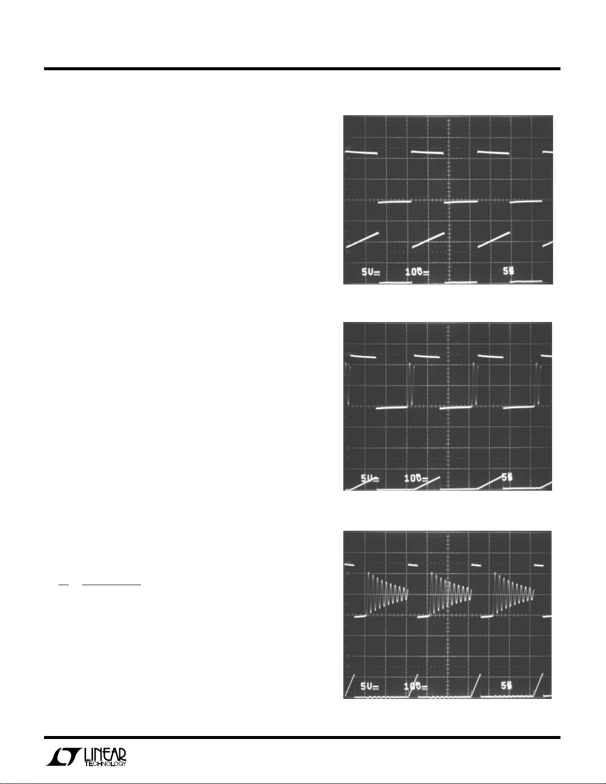
Switching Waveforms in Normal Mode
The waveforms in Figures 3 through 10 were taken with
an input voltage of 12V. Figure 3 shows the classic buck
converter waveforms of switch output voltage (5V/DIV) at
the top and switch current (1A/DIV) underneath, at an
output current of 2A. The regulator is operating in “continuous” mode as evidenced by the fact that switch
current does not start at zero at switch turn-on. Instead,
it jumps to an initial value, then continues to slope upward
during the duration of switch on time. The slope of the
current waveform is determined by the difference between input and output voltage, and the value of inductor
used.
V–V
()
dl
dt
=
IN OUT
L
According to theory, the average switch current during
switch on time should be equal to the 2A output current
and this is confirmed in the photograph. The peak switch
current, however, is about 2.4A.This peak current must
be considered when calculating maximum available load
current because both the LT1432 and the LT1070 family
current limit on instantaneous switch current.
5V/DIV
1A/DIV
5V/DIV
0.5A/DIV
0
0
0
0
5µs/DIV
Figure 4
5µs/DIV
Figure 5
9
 Loading...