

Linear Technology LT1425 Datasheet
FEATURES
OUTPUT CURRENT (mA)
0
OUTPUT VOLTAGE (V)
8.5
9.0
8.9
8.8
8.7
8.6
9.5
9.4
9.3
9.2
9.1
50 100
1425 TA02
150 200
■
No Transformer “Third Winding” or Optoisolator
Required
■
±5% Accurate Output Voltage Without User Trims
(See Circuit Below)
■
Resistor Programmable Output Voltage
■
Regulation Maintained Well Into Discontinuous
Mode (Light Load)
■
Optional Load Compensation
■
Operating Frequency: 285kHz
■
Easily Synchronized to External Clock
■
Available in 16-Pin Narrow SO Package
U
APPLICATIONS
■
Isolated Flyback Switching Regulators
■
Ethernet Isolated 5V to –9V Converters
■
Medical Instruments
■
Isolated Telecom Supplies
, LTC and LT are registered trademarks of Linear Technology Corporation.
LT1425
Isolated Flyback
Switching Regulator
U
DESCRIPTION
The LT®1425 is a monolithic high power switching regulator specifically designed for the isolated flyback topology. No “third winding” or optoisolator is required; the
integrated circuit senses the isolated output voltage
directly from the primary side flyback waveform. A high
current, high efficiency switch is included on the die along
with all oscillator, control and protection circuitry.
The LT1425 operates with input supply voltages from 3V
to 20V and draws only 7mA quiescent current. It can
deliver output power up to 6W with no external power
devices. By utilizing current mode switching techniques, it
provides excellent AC and DC line regulation.
The LT1425 has a number of features not found on other
switching regulator ICs. Its unique control circuitry can
maintain regulation well into discontinuous mode in most
applications. Optional load compensation circuitry allows
for improved load regulation. An externally activated shutdown mode reduces total supply current to 15µA for
standby operation.
TYPICAL APPLICATION
+
C1
100µF
10V
C3
1000pF
15
SHDN
6
SYNC
4
V
C
SGND PGND
5V to Isolated –9V
5V
12
V
IN
11
V
SW
LT1425
710
R
FB
R
REF
R
OCOMP
R
CCOMP
3
5
14
13
500V
ISOLATION BARRIER
T1*
D1
1N5819
••
R1
22.6k
1%
*DALE LPE 4841-330MB
R2
3.01k
1%
C4
0.1µF
R3
15k
U
OUT
C2
47µF
+
16V
1425 TA01
–
V
ISOLATED
–9V ±5% AT
20mA TO 200mA
F
Load Regulation
1

LT1425
WW
W
ABSOLUTE MAXIMUM RATINGS
U
U
W
PACKAGE/ORDER INFORMATION
(Note 1)
Supply Voltage ........................................................ 20V
Switch Voltage......................................................... 35V
SHDN, SYNC Pin Voltage........................................... 7V
RFB Pin Current....................................................... 2mA
Operating Junction Temperature Range
Commercial .......................................... 0°C to 100°C
Industrial ......................................... – 40°C to 100°C
Storage Temperature Range ................. –65°C to 150°C
Lead Temperature (Soldering, 10 sec).................. 300°C
1
GND
2
NC
3
R
FB
4
V
C
5
R
REF
6
SYNC
7
SGND
8
GND
16-LEAD PLASTIC SO
T
JMAX
TOP VIEW
16
15
14
13
12
11
10
9
S PACKAGE
= 145°C, θJA = 75°C/ W
GND
SHDN
R
OCOMP
R
CCOMP
V
IN
V
SW
PGND
GND
ORDER PART
NUMBER
LT1425CS
LT1425IS
Consult factory for Military grade parts.
ELECTRICAL CHARACTERISTICS
SYMBOL PARAMETER CONDITIONS MIN TYP MAX UNITS
Feedback Amplifier
I
REF
I
IN
g
m
I
SOURCE
V
CL
Output Switch
BV Output Switch Breakdown Voltage IC = 5mA ● 35 50 V
V(VSW) Output Switch ON Voltage ISW = 1A ● 0.55 0.85 V
I
LIM
Current Amplifier
Timing
f Switching Frequency 260 285 300 kHz
t
ON
t
ED
t
EN
Reference Current Measured at RFB Pin with R
R
Pin Input Current 500 nA
REF
Feedback Amplifier Transconductance ∆IC = ±10µA (Note 2) ● 400 1000 1600 µmho
, I
Feedback Amplifier Source or Sink Current ● 30 50 80 µA
SINK
Feedback Amplifier Clamp Voltage 1.9 V
Reference Voltage/Current Line Regulation 5V ≤ VIN ≤ 18V ● 0.01 0.04 %/V
Voltage Gain (Note 3) 500 V/V
VIN Sense Error ● 10 25 mV
Switch Current Limit Duty Cycle = 50%, 0°C ≤ TJ ≤ 100°C ● 1.35 1.60 1.9 A
Control Pin Threshold Duty Cycle = Minimum 0.95 1.2 1.3 V
Control Voltage to Switch Transconductance 2 A/V
Minimum Switch ON Time 170 210 260 ns
Flyback Enable Delay Time 150 ns
Minimum Flyback Enable Time 180 ns
Maximum Switch Duty Cycle ● 85 90 95 %
VIN = 5V, TJ = 25°C, VSW open, VC = 1.4V, unless otherwise specified.
= 3.000k 402 408 414 µA
REF
Duty Cycle = 50%, –40°C ≤ T
Duty Cycle = 80% 1.30 A
≤ 100°C ● 1.25 1.60 1.9 A
J
● 396 420 µA
● 0.85 1.4 V
● 240 320 kHz
U
2
LT1425
ELECTRICAL CHARACTERISTICS
VIN = 5V, TJ = 25°C, VSW Open, VC = 1.4V, unless otherwise specified.
SYMBOL PARAMETER CONDITIONS MIN TYP MAX UNITS
Load Compensation
∆V
RCCOMP
/∆I
SW
0.45 Ω
SYNC Function
Minimum SYNC Amplitude ● 1.5 2.2 V
Synchronization Range 320 450 kHz
SYNC Pin Input Resistance 40 kΩ
Power Supply
V
IN(MIN)
I
CC
Minimum Input Voltage ● 2.8 3.1 V
Supply Current ● 7.0 9.5 mA
Shutdown Mode Supply Current ● 15 40 µA
Shutdown Mode Threshold ● 0.4 0.9 1.3 V
The ● denotes the specifications which apply over the full operating
temperature range.
Note 2: Feedback amplifier transconductance is R
Note 3: Voltage gain is R
referred.
REF
referred.
REF
Note 1: Absolute Maximum Ratings are those values beyond which the life
of a device may be impaired.
UW
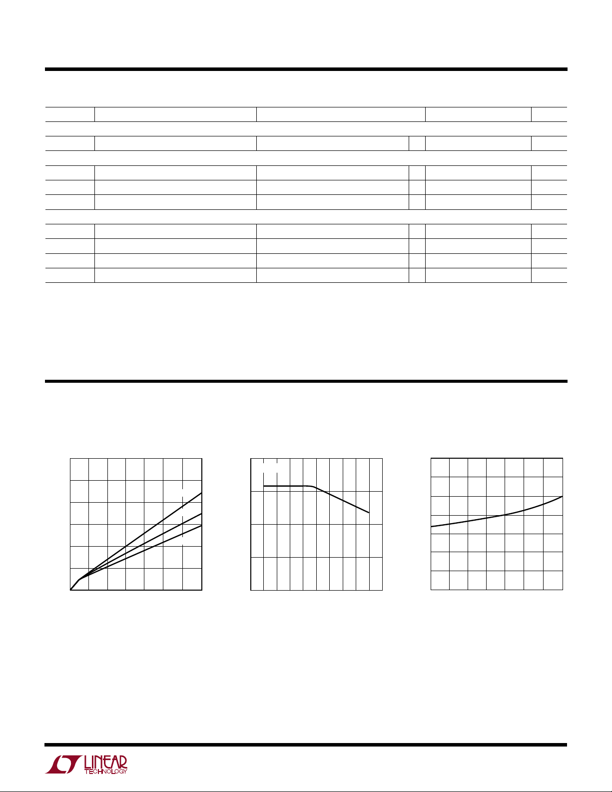
TYPICAL PERFORMANCE CHARACTERISTICS
Switch Saturation Voltage vs
Switch Current
1.2
1.0
0.8
0.6
0.4
0.2
SWITCH SATURATION VOLTAGE (V)
0
0
0.2 0.4
SWITCH CURRENT (A)
0.8 1.2 1.4
0.6 1.0
125°C
25°C
–55°C
1425 G01
Switch Current Limit vs
Duty Cycle
2.0
TA = 25°C
1.5
1.0
0.5
SWITCH CURRENT LIMIT (A)
0
102030
0
40
DUTY CYCLE (%)
50 60 70 80 90 100
1425 G02
Minimum Input Voltage vs
Temperature
3.1
3.0
2.9
2.8
2.7
INPUT VOLTAGE (V)
2.6
2.5
2.4
–50
–25 0
TEMPERATURE (°C)
50 100 125
25 75
1425 G03
3

LT1425
UW
TYPICAL PERFORMANCE CHARACTERISTICS
Feedback Amplifier Output
60
40
20
0
–20
–40
–60
FEEDBACK AMPLIFIER OUTPUT CURRENT (µA)
–80
1.05
Current vs R
1.10 1.15
REF
1.20 1.30
R
NODE VOLTAGE (V)
REF
Switching Frequency vs
Temperature
300
295
290
285
280
275
SWITCHING FREQUENCY (kHz)
270
Pin Voltage
25°C
125°C
–55°C
1.25 1.35 1.40
1425 G04
Error Amplifier Transconductance
vs Temperature (R
1400
1200
1000
800
600
400
TRANSCONDUCTANCE (µmho)
200
0
–50
–25 0
TEMPERATURE (°C)
REF
50 100 125
25 75
Minimum Synchronization
Voltage vs Temperature
)
2.50
P-P
2.25
2.00
1.75
1.50
1.25
1.00
Referred)
1425 G05
VC Pin Threshold and High Clamp
Voltage vs Temperature
2.50
2.25
2.00
1.75
1.50
PIN VOLTAGE (V)
C
V
1.25
1.00
0.75
–50
–25 0
VC HIGH CLAMP
VC THRESHOLD
50 100 125
25 75
TEMPERATURE (°C)
SHDN Pin Input Current vs
Voltage
1
TA = 25°C
0
–1
–2
–3
SHDN PIN INPUT CURRENT (µA)
1425 G06
265
–50
–25 0
25 75
TEMPERATURE (°C)
Minimum Switch ON Time vs
Temperature
300
275
250
225
200
175
SWITCH ON TIME (ns)
150
125
–50
–25 0
25 75
TEMPERATURE (°C)
4
50 100 125
1425 G07
50 100 125
1425 G10
MINIMUM SYNCHRONIZATION VOLTAGE (V
0.75
–50
–25 0
TEMPERATURE (°C)
50 100 125
25 75
Flyback Enable Delay Time vs
Temperature
250
225
200
175
150
125
ENABLE DELAY TIME (ns)
100
75
–50
–25 0
TEMPERATURE (°C)
50 100 125
25 75
1425 G08
1425 G11
–4
1
0
SHDN PIN VOLTAGE (V)
3
2
Minimum Flyback Enable Time vs
Temperature
275
250
225
200
175
ENABLE TIME (ns)
150
125
100
–50
–25 0
TEMPERATURE (°C)
50 100 125
25 75
4
5
1425 G09
1425 G12

PIN FUNCTIONS
LT1425
UUU
GND (Pins 1, 8, 9, 16): Ground. These pins connect to the
substrate of the die and are separate from the power
ground and signal ground. They should connect directly to
a good quality ground plane.
RFB (Pin 3): Input Pin for External “Feedback” Resistor
Connected to Transformer Primary (VSW). The ratio of this
resistor to the R
(VBG) reference, is the primary determinant of the output
voltage (plus the effect of any nonunity transformer turns
ratio). The average current through this resistor during the
flyback period should be approximately 400µ A. See Applications Information for more details.
VC (Pin 4): Control Voltage. This pin is the output of the
feedback amplifier and the input of the current comparator. Frequency compensation of the overall loop is effected
by placing a capacitor between this node and ground.
R
(Pin 5): Input Pin for External Ground-Referred
REF
“Reference” Resistor. This resistor should be in the range
of 3k, but for convenience, need not be this value precisely.
See Applications Information for more details.
SYNC (Pin 6): Pin to Synchronize Internal Oscillator to
External Frequency Reference. It is directly logic compatible and can be driven with any signal between 10% and
90% duty cycle. If unused, this pin can be left floating;
however, for best noise immunity the pin should be
grounded.
SGND (Pin 7): Signal Ground. This pin is a clean ground.
The internal reference and feedback amplifier are referred
to it. Keep the ground path connection to R
compensation capacitor free of large ground currents.
resistor, times the internal bandgap
REF
and the V
REF
C
PGND (Pin 10): Power Ground. This pin is the emitter of
the power switch device and has large currents flowing
through it. It should be connected directly to a good quality
ground plane.
VSW (Pin 11): This is the collector node of the output
switch and has large currents flowing through it. Keep the
traces to the switching components as short as possible
to minimize electromagnetic radiation and voltage spikes.
VIN (Pin 12): Supply Voltage. Bypass input supply pin with
10µ F or more. The part goes into undervoltage lockout
when VIN drops below 2.8V. Undervoltage lockout stops
switching and pulls the VC pin low.
R
Load Compensation Function. A common 0.1µF
ceramic capacitor will suffice for most applications. See
Applications Information for further details.
R
Compensation Resistor. Use of this pin allows nominal
compensation for nonzero output impedance in the power
transformer secondary circuit, including secondary winding impedance, output Schottky diode impedance and
output capacitor ESR. In less demanding applications this
resistor is not needed. See Applications Information for
more details.
SHDN (Pin 15): Shutdown. This pin is used to turn off the
regulator and reduce VIN input current to a few tens of
microamperes. The SHDN pin can be left floating when
unused.
(Pin 13): Pin for the External Filter Capacitor for
CCOMP
(Pin 14): Input Pin for Optional External Load
OCOMP
5
LT1425
BLOCK DIAGRAM
V
W
IN
R
FB
R
REF
SHDN
SYNC
2.6V
REGULATOR
285kHz
OSCILLATOR
COMP
SGND
GND IS OMITTED FOR CLARITY
WW
FLYBACK ERROR A PLIFIER DIAGRA
FLYBACK
ERROR
AMPLIFIER
COMPENSATION
V
C
LOAD
DRIVERLOGIC
R
OC0MP
R
CCOMP
CURRENT
AMPLIFIER
V
SW
+
R
SENSE
–
PGND
1425 BD
6
V
IN
V
SW
V
IN
D2
R
FB
R
FB
Q1
Q2 Q3
R
REF
I
R
REF
•
Q4
V
BG
D1
T1
•
+
C1
+
ISOLATED
V
OUT
–
I
M
I
FXD
V
C
ENABLE
C
EXT
I
M
1425 EA
 Loading...