

Linear Technology LT1413 Datasheet

LT1413
Single Supply, Dual
Precision Op Amp
EATU
F
RE
S
Single Supply Operation:
■
Input Goes Below Ground
■
Output Swings to Ground Sinking Current
■
No Pull-Down Resistors Needed
■
Phase Reversal Protection
At 5V, 0V Low Cost Grade Specifications:
■
280µV Max Offset Voltage
■
380µV Max in S8 Package
■
0.8nA Max Offset Current
■
480µA Max Supply Current per Amplifier
■
0.5µV/°C Drift
■
1.4 Million Voltage Gain
■
950kHz Gain-Bandwidth Product
■
0.55µV
PPLICATI
A
■
Single Supply Systems
■
Two and Three Op Amp Instrumentation Amplifiers
■
Active Filters
■
Battery-Powered Systems
■
Strain Gauge and Bridge Amplifiers
, 0.1Hz to 10Hz Noise
P-P
U
O
S
DUESCRIPTIO
The LT1413 is a low cost, upgraded version of Linear
Technology’s industry standard LT1013 dual, single supply op amp. The LT1413 is optimized for single 5V applications, although ± 15V specifications are also provided
for completeness.
In the design of the LT1413, particular emphasis has been
placed on low cost plastic and SO-8 package performance:
60µV offset voltage, 0.1nA offset current, in excess of
10mA output current at 330µ A supply current and 140dB
channel separation are some of the specifications achieved.
Other dual, single supply amplifiers are available to
complement the LT1413 family: the micropower LT1078’s
supply current is 10 times lower with a 4.5 fold speed
performance degradation compared to the LT1413. Conversely, the LT1211, LT1213 and LT1215 duals have 4 to
14 times higher supply current, but also 13 to 50 times
higher speed.
Protected by U.S. Patent 4,775,884.
10M
–
INPUT
10M
+
OUTPUT OFFSET =
(INPUT REFERRED =
INPUT RESISTANCE =
BANDWIDTH =
U
O
A
PPLICATITYPICAL
+90V, –3V Common-Mode Range
Difference Amplifier (AV = 1)
10M
9V
1M
1.5mV
125µV)
11M
80kHz
1M
10M
2
3
8
–
1/2 LT1413
+
(THE 0.1nA TYPICAL OFFSET CURRENT
PERMITS THE USE OF 1MΩ RESISTORS)
1
4
OUTPUT
20mV TO 8V
LT1413 • TA03
Distribution of Input Offset Voltage
(In Plastic DIP, N8 Package)
30
VS = 5V, 0V
= 25°C
T
A
25
20
15
10
PERCENT OF UNITS
5
0
–300
–100 0 100
–200
INPUT OFFSET VOLTAGE (µV)
200 300
LT1413 • TA01
1
LT1413
A
W
O
LUTEXI T
S
A
WUW
ARB
U
G
I
S
Supply Voltage ..................................................... ±22V
Differential Input Voltage ...................................... ±30V
Input Voltage ..................................................................
Equal to Positive Supply Voltage
5V Below Negative Supply Voltage
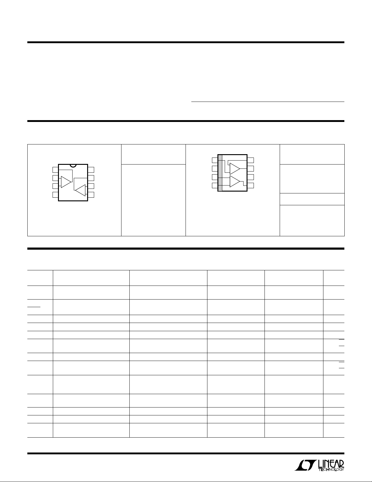
PACKAGE
/
O
RDER I FOR ATIO
WU
U
ORDER PART
NUMBER
LT1413ACN8
LT1413CN8
OUT A
1
–IN A
2
+IN A
3
–
V
4
8-LEAD PLASTIC DIP
T
JMAX
TOP VIEW
8
A
N8 PACKAGE
= 100°C, θJA = 130°C/W
7
6
B
5
V+
OUT B
–IN B
+IN B
Output Short-Circuit Duration ......................... Indefinite
Operating Temperature Range ............... – 40°C to 85°C
Storage Temperature Range ................ –65°C to 150°C
Lead Temperature (Soldering, 10 sec)................. 300°C
Note: When the input voltage exceeds the maximum ratings, the input current should be limited
to 10mA.
TOP VIEW
1
+IN A
–
V
2
+IN B
3
–IN B
4
8-LEAD PLASTIC SOIC
NOTE: THIS PIN CONFIGURATION DIFFERS FROM
THE 8-LEAD DIP PIN LOCATIONS. INSTEAD, IT
FOLLOWS THE INDUSTRY STANDARD LT1013DS8
SO PACKAGE CONFIGURATION.
T
JMAX
A
B
S8 PACKAGE
= 105°C, θJA = 200°C/ W
–IN A
8
OUT A
7
+
V
6
OUT B
5
ORDER PART
NUMBER
LT1413S8
S8 PART MARKING
1413
LECTRICAL C CHARA TERIST
E
SYMBOL PARAMETER CONDITIONS (Note 1) MIN TYP MAX MIN TYP MAX UNITS
V
OS
∆V
OS
∆Time Voltage Stability
I
OS
I
B
e
n
i
n
CMRR Common-Mode Rejection Ratio VCM = 0V to 3.65V 90 101 88 101 dB
PSRR Power Supply Rejection Ratio VS = 3.2V to 12V 102 118 100 118 dB
A
VOL
Input Offset Voltage LT1413N8 50 150 60 280 µV
Long-Term Input Offset 0.4 0.5 µV/Mo
Input Offset Current 0.1 0.7 0.1 0.8 nA
Input Bias Current 9 15 9 18 nA
Input Noise Voltage 0.1Hz to 10Hz (Note 2) 0.55 1.1 0.55 µV
Input Noise Voltage Density fO = 10Hz (Note 2) 24 38 24 nV/√Hz
Input Noise Current 0.1Hz to 10Hz 2.8 2.8 pA
Input Noise Current Density fO = 10Hz 0.07 0.07 pA/√Hz
Input Resistance (Note 3)
Differential Mode 300 500 250 500 MΩ
Common Mode 3 3 GΩ
Input Voltage Range 3.65 3.8 3.65 3.8 V
Large-Signal Voltage Gain VO = 0.05V to 4V, No Load 400 1400 350 1400 V/mV
ICS
VS = 5V, 0V, VCM = 0.1V, VO = 1.4V, TA = 25°C, unless otherwise noted.
LT1413ACN8
LT1413S8 80 380 µV
fO = 1000Hz (Note 2) 23 30 23 nV/√Hz
fO = 1000Hz 0.02 0.02 pA/√Hz
0 –0.3 0 –0.3 V
VO = 0.05V to 3.5V, RL = 2k 300 1000 250 1000 V/mV
LT1413CN8/S8
P-P
P-P
2
LT1413
LECTRICAL C CHARA TERIST
E
SYMBOL PARAMETER CONDITIONS MIN TYP MAX MIN TYP MAX UNITS
Maximum Output Voltage Swing Output Low, No Load 15 25 15 25 mV
SR Slew Rate AV = 1 0.2 0.3 0.2 0.3 V/µs
GBW Gain-Bandwidth Product fO ≤ 100kHz (Note 4) 600 950 600 950 kHz
I
S
Supply Current per Amplifier 330 450 330 480 µA
Channel Separation ∆VIN = 3V, RL = 2k (Note 5) 125 140 123 140 dB
Minimum Supply Voltage (Note 6) 2.85 3.0 2.85 3.0 V
Output Low, 600Ω to GND 5 10 5 10 mV
Output Low, I
Output High, No Load 4.1 4.4 4.1 4.4 V
Output High, 600Ω to GND 3.4 4.0 3.4 4.0 V
VS = 5V, 0V, VCM = 0.1V, VO = 1.4V, TA = 25°C, unless otherwise noted.
ICS
LT1413ACN8 LT1413CN8/S8
= 1mA 220 350 220 350 mV
SINK
VS = 5V, 0V, VCM = 0.1V, VO = 1.4V, 0°C ≤ TA ≤ 70°C, unless otherwise noted.
LT1413ACN8 LT1413CN8/S8
SYMBOL PARAMETER CONDITIONS (Note 1) MIN TYP MAX MIN TYP MAX UNITS
V
OS
∆VOS/∆T Input Offset Voltage Drift (Note 5) ● 0.3 2.0 0.4 2.5 µV/°C
I
OS
I
B
CMRR Common-Mode Rejection Ratio VCM = 0V to 3.6V ● 88 100 85 100 dB
PSRR Power Supply Rejection Ratio VS = 3.45V to 12V ● 100 117 97 117 dB
A
VOL
I
S
Input Offset Voltage LT1413N8 ● 65 240 80 390 µV
Input Offset Current ● 0.1 1.0 0.1 1.2 nA
Input Bias Current ● 10 20 10 23 nA
Large-Signal Voltage Gain VO = 0.07V to 3.9V, No Load ● 300 1100 300 1100 V/mV
Maximum Output Voltage Swing Output Low, No Load ● 18 32 18 32 mV
Supply Current per Amplifier ● 350 500 350 530 µA
LT1413S8
VO = 0.07V to 3.2V, RL = 2k ● 200 800 200 800 V/mV
Output Low, I
Output High, No Load ● 4.0 4.3 4.0 4.3 V
Output High, 600Ω to GND ● 3.3 3.9 3.2 3.9 V
= 1mA ● 270 430 270 430 mV
SINK
● 100 490 µV
VS = 5V, 0V, VCM = 0.1V, VO = 1.4V, –40°C ≤ TA ≤ 85°C (Note 7)
LT1413ACN8 LT1413CN8/S8
SYMBOL PARAMETER CONDITIONS (Note 1) MIN TYP MAX MIN TYP MAX UNITS
V
OS
∆VOS/∆T Input Offset Voltage Drift ● 0.3 2.2 0.4 2.8 µV/°C
I
OS
I
B
CMRR Common-Mode Rejection Ratio VCM = 0V to 3.4V ● 85 99 82 99 dB
PSRR Power Supply Rejection Ratio VS = 3.9V to 12V ● 98 116 94 116 dB
A
VOL
I
S
Input Offset Voltage LT1413N8 ● 70 300 85 470 µV
Input Offset Current ● 0.2 1.4 0.2 1.7 nA
Input Bias Current ● 11 25 11 30 nA
Large-Signal Voltage Gain VO = 0.08V to 3.8V, No Load ● 220 1000 220 1000 V/mV
Maximum Output Voltage Swing Output Low, No Load ● 20 38 20 38 mV
Supply Current per Amplifier ● 360 550 360 580 µA
LT1413S8
VO = 0.08V to 3.0V, RL = 2k ● 150 700 150 700 V/mV
Output Low, I
Output High, No Load ● 3.9 4.2 3.9 4.2 V
Output High, 600Ω to GND
= 1mA ● 300 480 300 480 mV
SINK
● 110 570 µV
● 3.1 3.8 3.0 3.8 V
3
 Loading...