

Linear Technology LT1399HV, LT1399, LT1398 Datasheet
FEATURES
■
300MHz Bandwidth on ±5V (A
■
0.1dB Gain Flatness: 150MHz (AV = 1, 2 and –1)
■
Completely Off in Shutdown, 0µA Supply Current
■
High Slew Rate: 800V/µs
■
Wide Supply Range:
= 1, 2 and –1)
V
±2V(4V) to ±6V(12V) (LT1398/LT1399)
±2V (4V) to ±7.5V (15V) (LT1399HV)
■
80mA Output Current
■
Low Supply Current: 4.6mA/Amplifier
■
Fast Turn-On Time: 30ns
■
Fast Turn-Off Time: 40ns
■
16-Pin Narrow SO/Narrow SSOP Packages
U
APPLICATIO S
LT1398/LT1399/LT1399HV
Low Cost Dual and Triple
300MHz Current Feedback
Amplifiers with Shutdown
U
DESCRIPTIO
The LT®1399 and LT1399HV contain three independent
300MHz current feedback amplifiers, each with a shutdown pin. The LT1399HV is a higher voltage version of the
LT1399. The LT1398 is a two amplifier version of the
LT1399.
The LT1398/LT1399 operate on all supplies from a single
4V to ±6V. The LT1399HV operates on all supplies from 4V
to ±7.5V.
Each amplifier draws 4.6mA when active. When disabled
each amplifier draws zero supply current and its output becomes high impedance. The amplifiers turn on in only 30ns
and turn off in 40ns, making them ideal in spread spectrum
and portable equipment applications.
■
RGB Cable Drivers
■
LCD Drivers
■
Spread Spectrum Amplifiers
■
MUX Amplifiers
■
Composite Video Cable Drivers
■
Portable Equipment
TYPICAL APPLICATIO
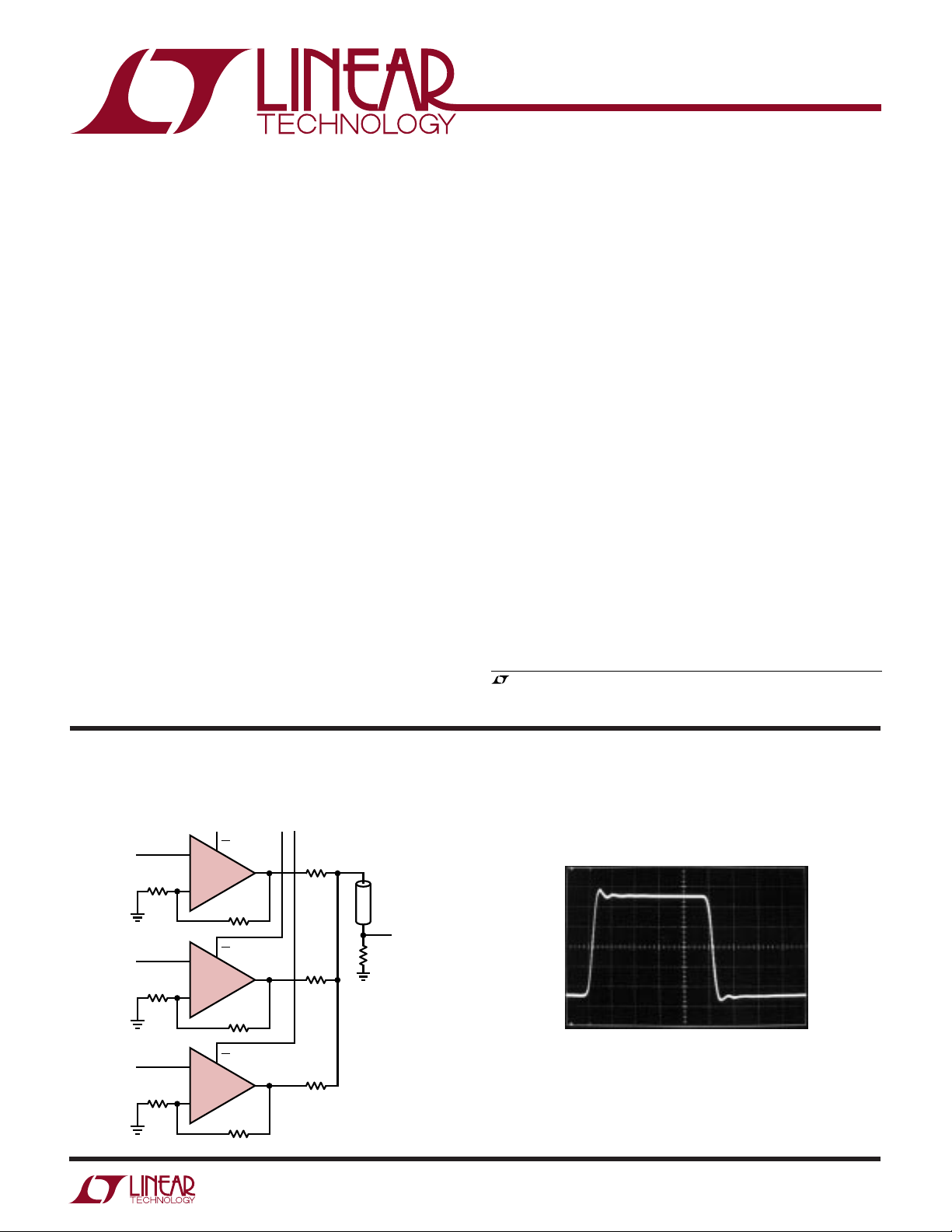
3-Input Video MUX Cable Driver
CHANNEL
A
V
IN A
R
G
200Ω
V
IN B
R
G
200Ω
V
IN C
R
G
200Ω
EN A
+
1/3 LT1399
–
EN B
+
1/3 LT1399
–
EN C
+
1/3 LT1399
–
324Ω
324Ω
324Ω
SELECT
R
F
R
F
R
F
BC
97.6Ω
97.6Ω
97.6Ω
U
1399 TA01
75Ω
75Ω
CABLE
The LT1398/LT1399/LT1399HV are manufactured on Linear Technology’s proprietary complementary bipolar process. The LT1399/LT1399HV are pin-for-pin upgrades to
the LT1260 optimized for use on ±5V/±7.5V supplies.
, LTC and LT are registered trademarks of Linear Technology Corporation.
Square Wave Response
V
OUT
OUTPUT
200mV/DIV
RL = 100Ω
= RG = 324Ω
R
F
f = 10MHz
TIME (10ns/DIV)
1398/99 TA02
1
LT1398/LT1399/LT1399HV
W
O
A
LUTEXI TIS
S
Total Supply Voltage (V+ to V–)
LT1398/LT1399 ................................................ 12.6V
LT1399HV ....................................................... 15.5V
Input Current (Note 2) ....................................... ±10mA
Output Current................................................. ±100mA
Differential Input Voltage (Note 2) ........................... ±5V
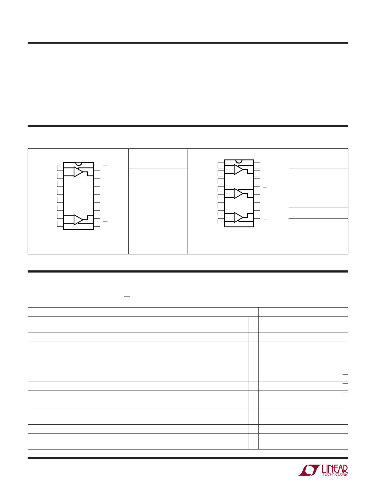
PACKAGE
1
–IN A
2
+IN A
3
*GND
4
*GND
5
*GND
6
*GND
7
+IN B
8
–IN B
16-LEAD PLASTIC SO
T
= 150°C, θJA = 100°C/W
JMAX
*Ground pins are not internally connected. For best channel isolation, connect to ground. Consult factory for Industrial and Military grade parts.
A
/
O
RDER I FOR ATIO
TOP VIEW
A
B
S PACKAGE
16
15
14
13
12
11
10
9
WUW
EN A
OUT A
+
V
GND*
GND*
–
V
OUT B
EN B
U
ARB
G
WU
ORDER PART
NUMBER
LT1398CS
(Note 1)
Output Short-Circuit Duration (Note 3)........ Continuous
Operating Temperature Range ............... – 40°C to 85°C
Specified Temperature Range (Note 4).. –40°C to 85°C
Storage Temperature Range ................ –65°C to 150°C
Junction Temperature (Note 5)............................ 150°C
Lead Temperature (Soldering, 10 sec)................. 300°C
U
TOP VIEW
1
–IN R
2
+IN R
3
*GND
4
–IN G
5
+IN G
6
*GND
7
+IN B
8
–IN B
GN PACKAGE
16-LEAD PLASTIC SSOP
T
= 150°C, θJA = 120°C/W (GN)
JMAX
= 150°C, θJA = 100°C/W (S)
T
JMAX
R
G
B
16
15
14
13
12
11
10
9
S PACKAGE
16-LEAD PLASTIC SO
EN R
OUT R
+
V
EN G
OUT G
–
V
OUT B
EN B
ORDER PART
NUMBER
LT1399CGN
LT1399CS
LT1399HVCS
GN PART MARKING
1399
LECTRICAL C CHARA TERIST
E
(LT1398/LT1399)
ICS
The ● denotes specifications which apply over the specified operating temperature range, otherwise specifications are at TA = 25°C.
For each amplifier: VCM = 0V, V
SYMBOL PARAMETER CONDITIONS MIN TYP MAX UNITS
V
OS
∆VOS/∆T Input Offset Voltage Drift ● 15 µV/°C
+
I
IN
–
I
IN
e
n
+i
n
–i
n
R
IN
C
IN
C
OUT
V
INH
Input Offset Voltage 1.5 10 mV
Noninverting Input Current 10 25 µA
Inverting Input Current 10 50 µA
Input Noise Voltage Density f = 1kHz, RF = 1k, RG = 10Ω, RS = 0Ω 4.5 nV/√Hz
Noninverting Input Noise Current Density f = 1kHz 6 pA/√Hz
Inverting Input Noise Current Density f = 1kHz 25 pA/√Hz
Input Resistance VIN = ±3.5V ● 0.3 1 MΩ
Input Capacitance Amplifier Enabled 2.0 pF
Output Capacitance Amplifier Disabled 8.5 pF
Input Voltage Range, High VS = ±5V ● 3.5 4.0 V
= ±5V, EN = 0V, pulse tested, unless otherwise noted. (Note 4)
S
● 12 mV
● 30 µA
● 60 µA
Amplifier Disabled 2.5 pF
V
= 5V, 0V 4.0 V
S
2
LT1398/LT1399/LT1399HV
LECTRICAL C CHARA TERIST
E
(LT1398/LT1399)
ICS
The ● denotes specifications which apply over the specified operating temperature range, otherwise specifications are at TA = 25°C.
For each amplifier: VCM = 0V, V
SYMBOL PARAMETER CONDITIONS MIN TYP MAX UNITS
V
INL
V
OUTH
V
OUTL
V
OUTH
V
OUTL
CMRR Common Mode Rejection Ratio VCM = ±3.5V ● 42 52 dB
–I
CMRR
PSRR Power Supply Rejection Ratio VS = ±2V to ±5V, EN = V
+I
PSRR
–I
PSRR
A
V
R
OL
I
OUT
I
S
I
EN
SR Slew Rate (Note 6) AV = 10, RL = 150Ω 500 800 V/µs
t
ON
t
OFF
tr, t
f
t
PD
os Small-Signal Overshoot RF = RG = 324Ω, RL = 100Ω, V
t
S
dG Differential Gain (Note 8) RF = RG = 324Ω, RL = 150Ω 0.13 %
dP Differential Phase (Note 8) RF = RG = 324Ω, RL = 150Ω 0.10 DEG
Input Voltage Range, Low VS = ±5V ● –3.5 –4.0 V
Maximum Output Voltage Swing, High VS = ±5V, RL = 100k 3.9 4.2 V
Maximum Output Voltage Swing, Low VS = ±5V, RL = 100k –3.9 – 4.2 V
Maximum Output Voltage Swing, High VS = ±5V, RL = 150Ω 3.4 3.6 V
Maximum Output Voltage Swing, Low VS = ±5V, RL = 150Ω –3.4 –3.6 V
Inverting Input Current VCM = ±3.5V 10 16 µA/V
Common Mode Rejection V
Noninverting Input Current VS = ±2V to ±5V, EN = V
Power Supply Rejection
Inverting Input Current VS = ±2V to ±5V, EN = V
Power Supply Rejection
Large-Signal Voltage Gain V
Transimpedance, ∆V
Maximum Output Current RL = 0Ω ● 80 mA
Supply Current per Amplifier V
Disable Supply Current per Amplifier EN Pin Voltage = 4.5V, RL = 150Ω ● 0.1 100 µA
Enable Pin Current 30 110 µA
Turn-On Delay Time (Note 7) RF = RG = 324Ω, RL = 100Ω 30 75 ns
Turn-Off Delay Time (Note 7) RF = RG = 324Ω, RL = 100Ω 40 100 ns
Small-Signal Rise and Fall Time RF = RG = 324Ω, RL = 100Ω, V
Propagation Delay RF = RG = 324Ω, RL = 100Ω, V
Settling Time 0.1%, AV = –1, RF = RG = 309Ω, RL = 150Ω 25 ns
= ±5V, EN = 0V, pulse tested, unless otherwise noted. (Note 4)
S
VS = 5V, 0V 1.0 V
V
= ±5V, RL = 100k ● 3.7 V
S
VS = 5V, 0V; RL = 100k 4.2 V
VS = ±5V, RL = 100k ● –3.7 V
V
= 5V, 0V; RL = 100k 0.8 V
S
VS = ±5V, RL = 150Ω ● 3.2 V
V
= 5V, 0V; RL = 150Ω 3.6 V
S
VS = ±5V, RL = 150Ω ● –3.2 V
V
= 5V, 0V; RL = 150Ω 0.6 V
S
= ±3.5V ● 22 µA/V
OUT
/∆I
CM
= ±2V, RL = 150Ω 50 65 dB
–
IN
OUT
V
= ±2V, RL = 150Ω 40 100 kΩ
OUT
= 0V ● 4.6 6.5 mA
OUT
–
–
–
= 1V
OUT
P-P
= 1V
OUT
P-P
= 1V
OUT
P-P
● 56 70 dB
12 µA/V
● 3 µA/V
● 27 µA/V
● 200 µA
1.3 ns
2.5 ns
10 %
3

LT1398/LT1399/LT1399HV
LECTRICAL C CHARA TERIST
E
ICS
(LT1399HV)
The ● denotes specifications which apply over the specified operating temperature range, otherwise specifications are at TA = 25°C.
For each amplifier: VCM = 0V, V
SYMBOL PARAMETER CONDITIONS MIN TYP MAX UNITS
V
OS
∆VOS/∆T Input Offset Voltage Drift ● 15 µV/°C
+
I
IN
–
I
IN
e
n
+i
n
–i
n
R
IN
C
IN
C
OUT
V
INH
V
INL
V
OUTH
V
OUTL
V
OUTH
V
OUTL
CMRR Common Mode Rejection Ratio VCM = ±6V ● 42 52 dB
–I
CMRR
PSRR Power Supply Rejection Ratio VS = ±2V to ±7.5V, EN = V
+I
PSRR
–I
PSRR
A
V
R
OL
I
OUT
I
S
I
EN
Input Offset Voltage 1.5 10 mV
Noninverting Input Current 10 25 µA
Inverting Input Current 10 50 µA
Input Noise Voltage Density f = 1kHz, RF = 1k, RG = 10Ω, RS = 0Ω, VS = ±5V 4.5 nV/√Hz
Noninverting Input Noise Current Density f = 1kHz, VS = ±5V 6 pA/√Hz
Inverting Input Noise Current Density f = 1kHz, VS = ±5V 25 pA/√Hz
Input Resistance VIN = ±6V ● 0.3 1 MΩ
Input Capacitance Amplifier Enabled 2.0 pF
Output Capacitance Amplifier Disabled 8.5 pF
Input Voltage Range, High VS = ±7.5V ● 6 6.5 V
Input Voltage Range, Low VS = ±7.5V ● –6 –6.5 V
Maximum Output Voltage Swing, High VS = ±7.5V, RL = 100k 6.4 6.7 V
Maximum Output Voltage Swing, Low VS = ±7.5V, RL = 100k –6.4 –6.7 V
Maximum Output Voltage Swing, High VS = ±7.5V, RL = 150Ω 5.4 5.8 V
Maximum Output Voltage Swing, Low VS = ±7.5V, RL = 150Ω – 5.4 –5.8 V
Inverting Input Current VCM = ±6V 10 16 µA/V
Common Mode Rejection V
Noninverting Input Current VS = ±2V to ±7.5V, EN = V
Power Supply Rejection
Inverting Input Current VS = ±2V to ±7.5V, EN = V
Power Supply Rejection
Large-Signal Voltage Gain V
Transimpedance, ∆V
Maximum Output Current RL = 0Ω ● 80 mA
Supply Current per Amplifier V
Disable Supply Current per Amplifier EN Pin Voltage = 7V, RL = 150Ω ● 0.1 100 µA
Enable Pin Current 30 110 µA
= ±7.5V, EN = 0V, pulse tested, unless otherwise noted. (Note 4)
S
Amplifier Disabled 2.5 pF
= 7.5V, 0V 6.5 V
V
S
VS = 7.5V, 0V 1.0 V
V
= ±7.5V, RL = 100k ● 6.1 V
S
VS = 7.5V, 0V; RL = 100k 6.7 V
VS = ±7.5V, RL = 100k ● –6.1 V
V
= 7.5V, 0V; RL = 100k 0.8 V
S
VS = ±7.5V, RL = 150Ω ● 5.1 V
V
= 7.5V, 0V; RL = 150Ω 5.8 V
S
VS = ±7.5V, RL = 150Ω ● – 5.1 V
V
= 7.5V, 0V; RL = 150Ω 0.6 V
S
= ±6V ● 22 µA/V
OUT
/∆I
CM
= ±4.5V, RL = 150Ω 50 65 dB
–
IN
OUT
V
= ±4.5V, RL = 150Ω 40 100 kΩ
OUT
= 0V ● 4.6 7 mA
OUT
–
–
–
● 12 mV
● 30 µA
● 60 µA
● 56 70 dB
12 µA/V
● 3 µA/V
● 27 µA/V
● 200 µA
4
LT1398/LT1399/LT1399HV
LECTRICAL C CHARA TERIST
E
ICS
(LT1399HV)
The ● denotes specifications which apply over the specified operating temperature range, otherwise specifications are at TA = 25°C.
For each amplifier: VCM = 0V, V
SYMBOL PARAMETER CONDITIONS MIN TYP MAX UNITS
SR Slew Rate (Note 6) AV = 10, RL = 150Ω, VS = ±5V 500 800 V/µs
t
ON
t
OFF
tr, t
f
t
PD
os Small-Signal Overshoot RF = RG = 324Ω, RL = 100Ω, V
t
S
dG Differential Gain (Note 8) RF = RG = 324Ω, RL = 150Ω, VS = ±5V 0.13 %
dP Differential Phase (Note 8) RF = RG = 324Ω, RL = 150Ω, VS = ±5V 0.10 DEG
Note 1: Absolute Maximum Ratings are those values beyond which the life
of a device may be impaired.
Note 2: This parameter is guaranteed to meet specified performance
through design and characterization. It has not been tested.
Note 3: A heat sink may be required depending on the power supply
voltage and how many amplifiers have their outputs short circuited.
Note 4: The LT1398/LT1399/LT1399HV are guaranteed to meet specified
performance from 0°C to 70°C and are designed, characterized and
expected to meet these extended temperature limits, but are not tested at
–40°C and 85°C. Guaranteed I grade parts are available, consult factory.
Note 5: TJ is calculated from the ambient temperature TA and the
power dissipation P
LT1398CS, LT1399CS, LT1399HVCS: T
LT1399CGN: T
Turn-On Delay Time (Note 7) RF = RG = 324Ω, RL = 100Ω, VS = ±5V 30 75 ns
Turn-Off Delay Time (Note 7) RF = RG = 324Ω, RL = 100Ω, VS = ±5V 40 100 ns
Small-Signal Rise and Fall Time RF = RG = 324Ω, RL = 100Ω, V
Propagation Delay RF = RG = 324Ω, RL = 100Ω, V
Settling Time 0.1%, AV = –1V, RF = RG = 309Ω, RL = 150Ω,25ns
according to the following formula:
D
= TA + (PD • 120°C/W)
J
= ±7.5V, EN = 0V, pulse tested, unless otherwise noted. (Note 4)
S
= 1V
, 1.3 ns
P-P
= 1V
, 2.5 ns
P-P
= 1V
,10%
P-P
= 0.5V. This specification is guaranteed by design
IN
V
= ±5V
S
VS = ±5V
V
= ±5V
S
V
= ±5V
S
= TA + (PD • 100°C/W)
J
OUT
OUT
OUT
Note 6: Slew rate is measured at ±2V on a ±3V output signal.
Note 7: Turn-on delay time (tON) is measured from control input to
appearance of 1V at the output, for V
time (t
the output for V
and characterization.
Note 8: Differential gain and phase are measured using a Tektronix
TSG120YC/NTSC signal generator and a Tektronix 1780R Video
Measurement Set. The resolution of this equipment is 0.1% and 0.1°.
Ten identical amplifier stages were cascaded giving an effective
resolution of 0.01% and 0.01°.
) is measured from control input to appearance of 0.5V on
OFF
= 1V. Likewise, turn-off delay
IN
U
W
TYPICAL AC PERFOR A CE
SMALL SIGNAL SMALL SIGNAL SMALL SIGNAL
(V) A
V
S
±5 1 100 365 – 300 150 0.05
±5 2 100 324 324 300 150 0
±5 –1 100 309 309 300 150 0
V
R
(Ω)R
L
F
(Ω)R
(Ω) – 3dB BW (MHz) 0.1dB BW (MHz) PEAKING (dB)
G
5
 Loading...