

Linear Technology LT1394 Datasheet
LT1394
7ns, Low Power,
Single Supply, Ground-Sensing
FEATURES
■
UltraFastTM: 7ns
■
Low Power: 6mA
■
Low Offset Voltage: 0.8mV
■
Operates Off Single 5V or Dual ±5V Supplies
■
Input Common Mode Extends to Negative Supply
■
No Minimum Input Slew Rate Requirement
■
Complementary TTL Outputs
■
Inputs Can Exceed Supplies without Phase Reversal
■
Pin Compatible with LT1016, LT1116 and LT1671
■
Output Latch Capability
■
Available in 8-Lead MSOP and SO Packages
U
APPLICATIO S
■
High Speed A/D Converters
■
Zero-Crossing Detectors
■
Current Sense for Switching Regulators
■
Extended Range V/F Coverters
■
Fast Pulse Height/Width Discriminators
■
High Speed Triggers
■
Line Receivers
■
High Speed Sampling Circuits
, LTC and LT are registered trademarks of Linear Technology Corporation.
UltraFast is a trademark of Linear Technology Corporation.
U
Comparator
DESCRIPTIO
The LT®1394 is an UltraFast (7ns) comparator with complementary outputs and latch. The input common mode range
extends from 1.5V below the positive supply down to the
negative supply rail. Like the LT1016, LT1116 and LT1671,
this comparator has complementary outputs designed to
interface directly to TTL or CMOS logic. The LT1394 may
operate from either a single 5V supply or dual ±5V supplies.
Low offset voltage specifications and high gain allow the
LT1394 to be used in precision applications.
The LT1394 is designed for improved speed and stability for
a wide range of operating conditions. The output stage
provides active drive in both directions for maximum speed
into TTL, CMOS or passive loads with minimal cross-conduction current. Unlike other fast comparators, the LT1394
remains stable even for slow transitions through the active
region, which eliminates the need to specify a minimum input
slew rate.
The LT1394 has an internal, TTL/CMOS compatible latch for
retaining data at the outputs. The latch holds data as long as
the LATCH pin is held high. Device parameters such as gain,
offset and negative power supply current are not significantly
affected by variations in negative supply voltage.
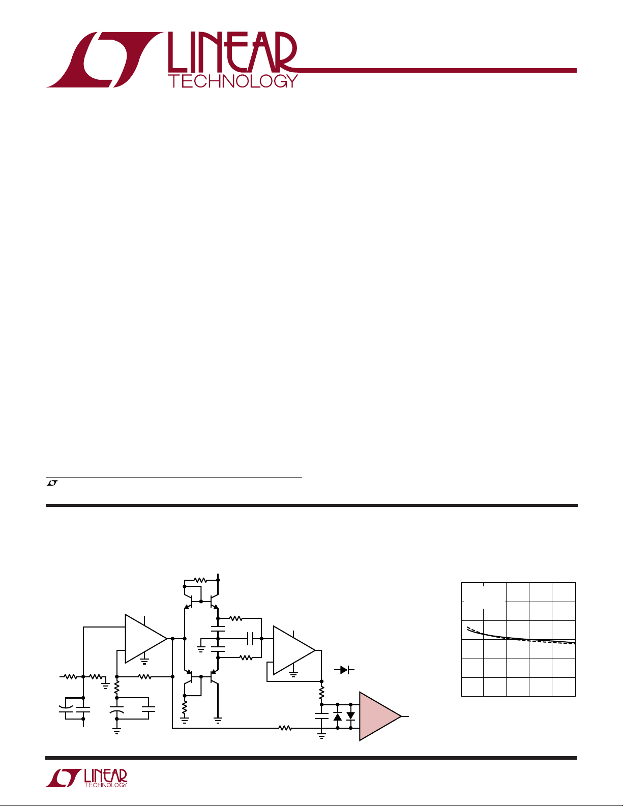
TYPICAL APPLICATIO
45MHz Single Supply Adaptive Trigger
3
Q1 Q2
10µF
5V
+
A1
LT1227
–
750Ω
2k
5V
+
0.1µF
INPUT
510Ω
36Ω
+
100µF
0.1µF
2
13
Q3
15
2k
2k
1
0.005µF
14
U
Propagation Delay vs
5V
6
5
3M
4
500pF
0.005µF
10
12
11
3M
Q4
+
LT1006
–
470Ω
5V
A2
0.1µF
Q1, Q2, Q3, Q4 = CA3096 ARRAY:
TIE SUBSTRATE (PIN 16) TO GROUND
470Ω
= 1N4148
+
LT1394
–
TRIGGER
OUT
1394 F18
12
10
8
6
TIME (ns)
4
2
0
Input Overdrive
TA = 25°C
= 100mV
V
STEP
= ±5V
V
S
0
10 20 30 40
OVERDRIVE (mV)
t
PDLH
t
PDHL
50
1394 TA02
1
LT1394
TOP VIEW
Q OUT
Q OUT
GND
V
+
+IN
–IN
V
–
S8 PACKAGE
8-LEAD PLASTIC SO
1
2
3
4
8
7
6
5
+
–
LATCH
ENABLE
WW
W
ABSOLUTE MAXIMUM RATINGS
U
(Note 1)
Total Supply Voltage (V+ to V–) ............................... 12V
Positive Supply Voltage ............................................. 7V
Negative Supply Voltage .......................................... –7V
Differential Input Voltage ....................................... ±12V
Input and Latch Current (Note 2)........................±10mA
Output Current (Continuous)(Note 2) .................±20mA
U
W
PACKAGE/ORDER INFORMATION
TOP VIEW
+
V
1
2
+IN
3
–IN
–
4
V
MS8 PACKAGE
8-LEAD PLASTIC MSOP
T
= 150°C, θJA = 250°C/W
JMAX
8
Q OUT
7
Q OUT
6
GND
5
LATCH
ENABLE
ORDER PART
NUMBER
LT1394CMS8
MS8 PART MARKING
LTBH
Operating Temperature Range ................ –40°C to 85°C
Specified Temperature Range (Note 3)... –40°C to 85°C
Junction Temperature........................................... 150°C
Storage Temperature Range ................. –65°C to 150°C
Lead Temperature (Soldering, 10 sec).................. 300°C
U
ORDER PART
NUMBER
LT1394CS8
LT1394IS8
S8 PART MARKING
T
= 150°C, θJA = 190°C/W
JMAX
1394
1394I
Consult factory for Military grade parts.
ELECTRICAL CHARACTERISTICS
The ● denotes specifications which apply over the full operating temperature range, otherwise specifications are TA = 25°C.
V+ = 5V, V– = –5V, V
SYMBOL PARAMETER CONDITIONS MIN TYP MAX UNITS
V
OS
∆V
OS
∆T
I
OS
I
B
V
CMR
CMRR Common Mode Rejection Ratio –5V ≤ VCM ≤ 3.5V, TA > 0°C 55 100 dB
PSRR Power Supply Rejection Ratio 4.6V ≤ V+ ≤ 5.4V ● 50 65 dB
A
V
V
OH
2
Input Offset Voltage RS ≤ 100Ω (Note 4) 0.8 2.5 mV
Input Offset Voltage Drift ● 4 µV/°C
Input Offset Current 0.1 0.5 µA
Input Bias Current (Note 5) 2 4.5 µA
Input Voltage Range (Note 6) ● –5 3.5 V
Small Signal Voltage Gain 1V ≤ V
Output Voltage Swing High V+ ≥ 4.6V, I
(Q) = 1.4V, V
OUT
= VCM = 0V unless otherwise noted.
LATCH
Single 5V Supply
–5V ≤ V
Single 5V Supply
0V ≤ V
0V ≤ V
–7V ≤ V
+
V
≤ 3.3V, TA ≤ 0°C55 dB
CM
≤ 3.5V, TA > 0°C 55 100 dB
CM
≤ 3.3V, TA ≤ 0°C55 dB
CM
–
≤ –2V ● 65 100 dB
≤ 2V 750 1600 V/V
OUT
≥ 4.6V, I
OUT
OUT
● 4.0 mV
● 0.8 µA
● 7.0 µA
● 0 3.5 V
= 1mA ● 2.7 3.1 V
= 4mA ● 2.4 3.0 V
LT1394
ELECTRICAL CHARACTERISTICS
The ● denotes specifications which apply over the full operating temperature range, otherwise specifications are TA = 25°C.
V+ = 5V, V– = –5V, V
SYMBOL PARAMETER CONDITIONS MIN TYP MAX UNITS
V
OL
+
I
–
I
V
IH
V
IL
I
IL
t
PD
∆t
PD
t
LPD
t
SU
t
H
t
PW(D)
Note 1: Absolute Maximum Ratings are those values beyond which the life
of a device may be impaired.
Note 2: This parameter is guaranteed to meet specified perforamnce
through design and characterization. It has not been tested.
Note 3: The LT1394CMS8 and LT1394CS8 are guaranteed to meet
specified performance from 0°C to 70°C and are designed, characterized
and expected to meet these extended temperature limits, but are not tested
at –40°C and 85°C. The LT1394IS8 is guaranteed to meet the extended
temperature limits.
Note 4: Input offset voltage (V
voltages measured by forcing first one output, then the other to 1.4V.
Note 5: Input bias current (I
currents.
Note 6: Input voltage range is guaranteed in part by CMRR testing and in
part by design and characterization.
Output Voltage Swing Low I
Positive Supply Current 6 8.5 mA
Negative Supply Current 1.2 2.2 mA
LATCH Pin High Input Voltage ● 2V
LATCH Pin Low Input Voltage ● 0.8 V
LATCH Pin Current V
Propagation Delay (Note 7) ∆VIN = 100mV, VOD = 5mV 7 9 ns
Differential Propagation Delay (Note 7) ∆VIN = 100mV, VOD = 5mV 0.5 2.2 ns
Latch Propagation Delay (Note 8) 6 ns
Latch Setup Time (Note 8) –0.4 ns
Latch Hold Time (Note 8) 2ns
Minimum Disable Pulse Width 3ns
(Q) = 1.4V, V
OUT
) is defined as the average of the two
OS
) is defined as the average of the two input
B
= VCM = 0V unless otherwise noted.
LATCH
= –4mA ● 0.3 0.5 V
OUT
I
= –10mA 0.4 V
OUT
● 10.0 mA
● 2.5 mA
= 0V ● –4 –10 µA
LATCH
● 14 ns
Note 7: t
and ∆tPD cannot be measured in automatic handling
PD
equipment with low values of overdrive. The LT1394 is 100% tested with a
100mV step and 20mV overdrive. Correlation tests have shown that t
and ∆tPD limits can be guaranteed with this test, if additional DC tests are
performed to guarantee that all internal bias conditions are correct.
Propagation delay (tPD) is measured with the overdrive added to the actual
. Differential propagation delay is defined as:
V
OS
∆tPD = t
Note 8: Latch propagation delay (t
respond when the LATCH pin is deasserted. Latch setup time (t
PDLH
– t
PDHL
) is the delay time for the output to
LPD
SU
interval in which the input signal must remain stable prior to asserting the
latch signal. Latch hold time (tH) is the interval after the latch is asserted in
which the input signal must remain stable.
PD
) is the
3
LT1394
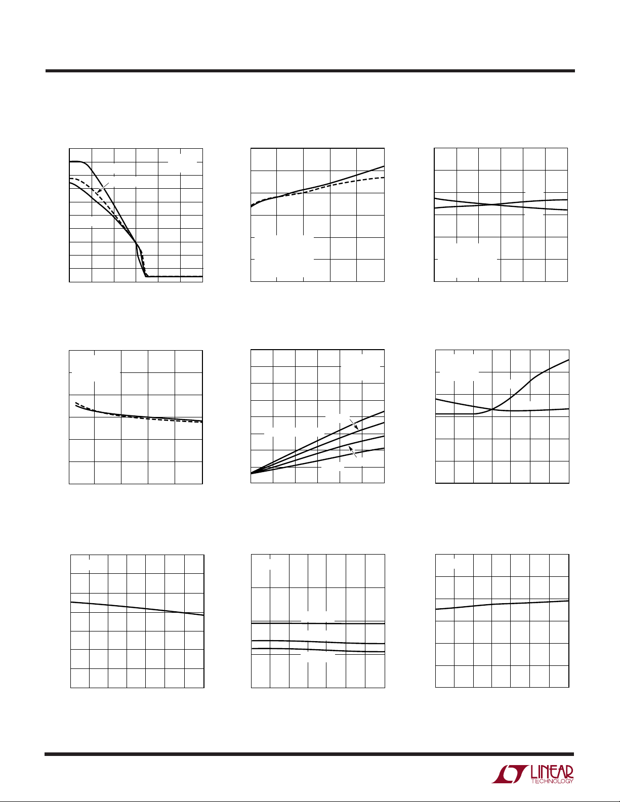
POSITIVE SUPPLY VOLTAGE (V)
4.4
TIME (ns)
12
10
8
6
4
2
0
4.6 4.8 5.0 5.2 5.4
1394 G03
5.6
t
PDHL
t
PDLH
V– = –5V
T
A
= 25°C
V
STEP
= 100mV
OVERDRIVE = 5mV
W
U
TYPICAL PERFORMANCE CHARACTERISTICS
Gain Characteristics
5.0
4.5
4.0
3.5
3.0
2.5
2.0
1.5
OUTPUT VOLTAGE (V)
1.0
0.5
0
TA = 125°C
TA = 25°C
TA = –55°C
–3
–2
–1
DIFFERENTIAL INPUT VOLTAGE (mV)
Propagation Delay vs
Input Overdrive
12
TA = 25°C
= 100mV
V
STEP
10
= ±5V
V
S
8
6
TIME (ns)
4
2
0
10 20 30 40
0
OVERDRIVE (mV)
01
t
PDLH
t
PDHL
VS = ±5V
= 0
I
OUT
2
1394 G01
1394 TA02
Propagation Delay vs
Load Capacitance
12
10
8
6
TIME (ns)
4
I
= 0
OUT
V
= ±5V
S
= 25°C
T
A
2
= 100mV
V
STEP
OVERDRIVE = 5mV
0
10 20 30 40
3
0
OUTPUT LOAD CAPACITANCE (pF)
t
PDLH
t
PDHL
50
1394 G02
Propagation Delay vs
Source Resistance
80
70
60
50
40
TIME (ns)
50
30
20
10
0
0 0.5
STEP SIZE = 800mV
1.0 2.01.5
SOURCE RESISTANCE (kΩ)
400mV
100mV
VS = ±5V
= 20mV
V
OD
= 25°C
T
A
200mV
2.5
3.0
1394 G04
Propagation Delay vs
Positive Supply Voltage
Propagation Delay vs
Temperature
12
VS = ±5V
= 100mV
V
STEP
10
= 5mV
V
OD
8
6
TIME (ns)
4
2
0
–50
–25 0
TEMPERATURE (°C)
t
PDLH
t
PDHL
50 100 125
25 75
1394 G05
Input Offset Voltage vs
Temperature
2
VS = ±5V
1
0
–1
–2
VOLTAGE (mV)
–3
–4
–5
–50 25 75
–25 0
TEMPERATURE (°C)
4
50 100 125
LT1394 G06
Input Bias Current vs
Temperature
4
VS = ±5V
3
2
1
INPUT BIAS CURRENT (µA)
0
–50 25 75
–25 0
VCM = –5V
VCM = 0V
VCM = 3.5V
TEMPERATURE (°C)
50 100 125
LT1394 G07
Positive Common Mode Limit vs
Temperature
6
VS = ±5V
5
4
3
VOLTAGE (V)
2
1
0
–50
–25 0
TEMPERATURE (°C)
50 100 125
25 75
1394 G08
W
U
TYPICAL PERFORMANCE CHARACTERISTICS
LT1394
Negative Common Mode Limit vs
Temperature
1
0
–1
–2
–3
INPUT VOLTAGE (V)
–4
–5
–6
–50 25 75
–25 0
VS = SINGLE 5V
VS = ±5V
50 100 125
TEMPERATURE (°C)
Positive Supply Current vs
V+ Supply Voltage
10
V– = 0V
9
= –60mV
V
IN
= 0
I
8
OUT
7
6
TA = 125°C
5
4
TA = 25°C
CURRENT (mA)
3
2
1
0
0
13
2
TA = –55°C
4
SUPPLY VOLTAGE (V)
5
Output Low Voltage (VOL) vs
Output Sink Current
0.8
VS = ±5V
LT1394 G09
0.7
0.6
0.5
0.4
VOLTAGE (V)
0.3
0.2
0.1
= 30mV
∆V
IN
TA = 125°C
TA = –55°C
0
02 6 10 14
4
OUTPUT SINK CURRENT (mA)
TA = 25°C
8
12
16
1394 G10
Positive Supply Current vs
Switching Frequency
16
VS = ±5V
14
12
10
TA = 125°C
8
6
CURRENT (mA)
TA = –55°C
4
2
0
7
6
8
1394 G12
1
SWITCHING FREQUENCY (MHz)
TA = 25°C
10 100
1394 G13
Output High Voltage (VOH) vs
Output Source Current
5.0
VS = ±5V
4.5
4.0
3.5
3.0
2.5
OUTPUT VOLTAGE (V)
2.0
1.5
1.0
= –30mV
∆V
IN
TA = 125°C
TA = 25°C
TA = –55°C
02 6 10 14
4
OUTPUT SOURCE CURRENT (mA)
8
Negative Supply Current vs
V– Supply Voltage
4
+
V
= 5V
∆V
= –60mV
IN
3
2
CURRENT (mA)
1
0
–7 –5 –3
–8
TA = 125°C
TA = 25°C
TA = –55°C
–6
NEGATIVE SUPPLY VOLTAGE (V)
–4
–1
16
1394 G11
0
1394 G14
12
–2
Latch Pin Current vs Temperature
8
VS = ±5V
7
6
5
4
3
CURRENT (µA)
2
1
0
= 0V
V
LATCH
–50 25 75
–25 0
TEMPERATURE (°C)
50 100 125
LT1394 G15
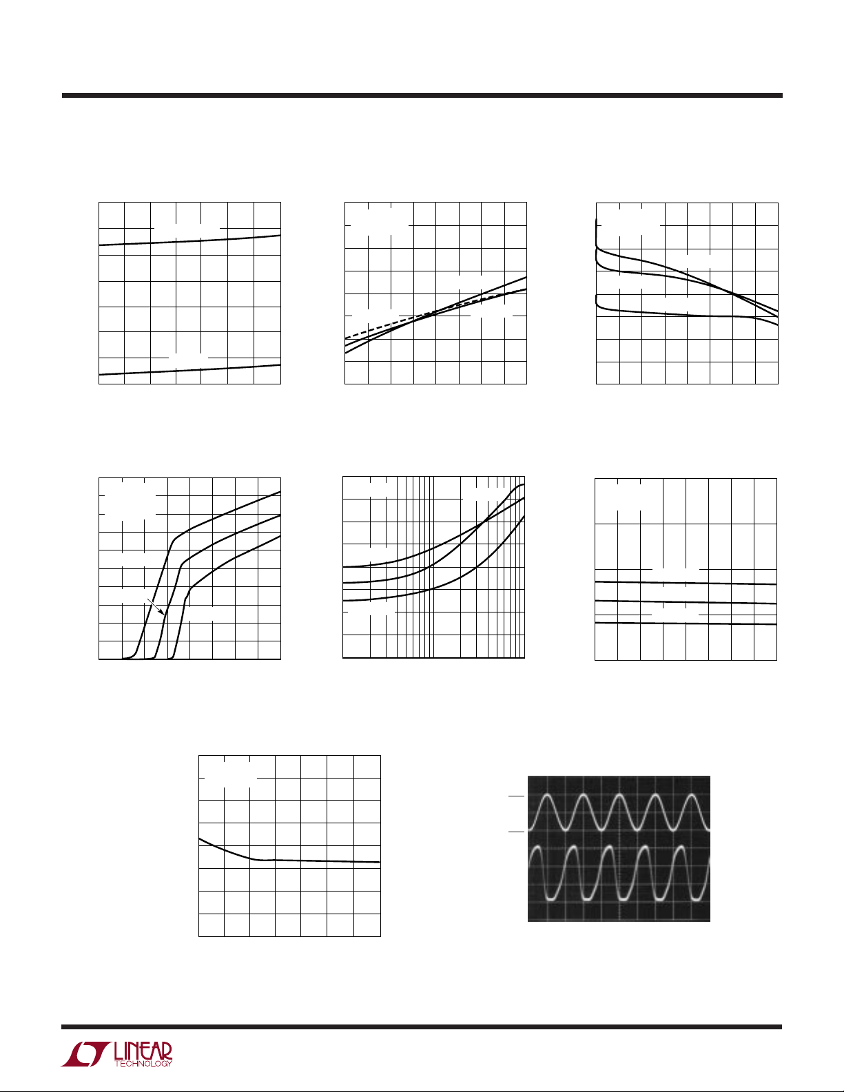
Response to 100MHz ±10mV
Sine Wave
+IN
20mV
P-P
3V
Q
OUT
0V
FET PROBES 5ns/DIV
10mV/DIV
1V/DIV
1394 G16
5
 Loading...