

Linear Technology LT1357 Datasheet

FEATURES
■
25MHz Gain Bandwidth
■
600V/µs Slew Rate
■
2.5mA Maximum Supply Current
■
Unity-Gain Stable
■
C-LoadTM Op Amp Drives All Capacitive Loads
■
8nV/√Hz Input Noise Voltage
■
600µV Maximum Input Offset Voltage
■
500nA Maximum Input Bias Current
■
120nA Maximum Input Offset Current
■
20V/mV Minimum DC Gain, RL=1k
■
115ns Settling Time to 0.1%, 10V Step
■
220ns Settling Time to 0.01%, 10V Step
■
±12V Minimum Output Swing into 500Ω
■
±2.5V Minimum Output Swing into 150Ω
■
Specified at ±2.5V, ±5V, and ±15V
U
APPLICATIONS
■
Wideband Amplifiers
■
Buffers
■
Active Filters
■
Data Acquisition Systems
■
Photodiode Amplifiers
, LTC and LT are registered trademarks of Linear Technology Corporation.
C-Load is a trademark of Linear Technology Corporation
LT1357
25MHz, 600V/µs Op Amp
U
DESCRIPTION
The LT®1357 is a high speed, very high slew rate operational amplifier with outstanding AC and DC performance.
The LT1357 has much lower supply current, lower input
offset voltage, lower input bias current, and higher DC gain
than devices with comparable bandwidth. The circuit
topology is a voltage feedback amplifier with the
slewing characteristics of a current feedback amplifier.
The amplifier is a single gain stage with outstanding
settling characteristics which makes the circuit an ideal
choice for data acquisition systems. The output drives a
500Ω load to ±12V with ±15V supplies and a 150Ω
load to ±2.5V on ±5V supplies. The amplifier is also
stable with any capacitive load which makes it useful in
buffer or cable driver applications.
The LT1357 is a member of a family of fast, high performance amplifiers using this unique topology and employing Linear Technology Corporation’s advanced bipolar
complementary processing. For dual and quad amplifier
versions of the LT1357 see the LT1358/LT1359 data
sheet. For higher bandwidth devices with higher supply
current see the LT1360 through LT1365 data sheets. For
lower supply current amplifiers see the LT1354 and LT1355/
LT1356 data sheets. Singles, duals, and quads of each
amplifier are available.
TYPICAL APPLICATION
DAC I-to-V Converter
6pF
DAC
INPUTS
12
5k
565A-TYPE
0.1µF5k
U
–
LT1357
+
VIk
+
()
OS OS
V
OUT
+<51Ω
A
VOL
1357 TA01
V
LSB
AV = –1 Large-Signal Response
OUT
1357 TA02
1
LT1357
WW
W
U
ABSOLUTE MAXIMUM RATINGS
Total Supply Voltage (V+ to V–) ............................... 36V
Differential Input Voltage (Transient Only, Note 1)...
±10V
Input Voltage ............................................................±V
Output Short-Circuit Duration (Note 2)............ Indefinite
Operating Temperature Range ................ –40°C to 85°C
U
W
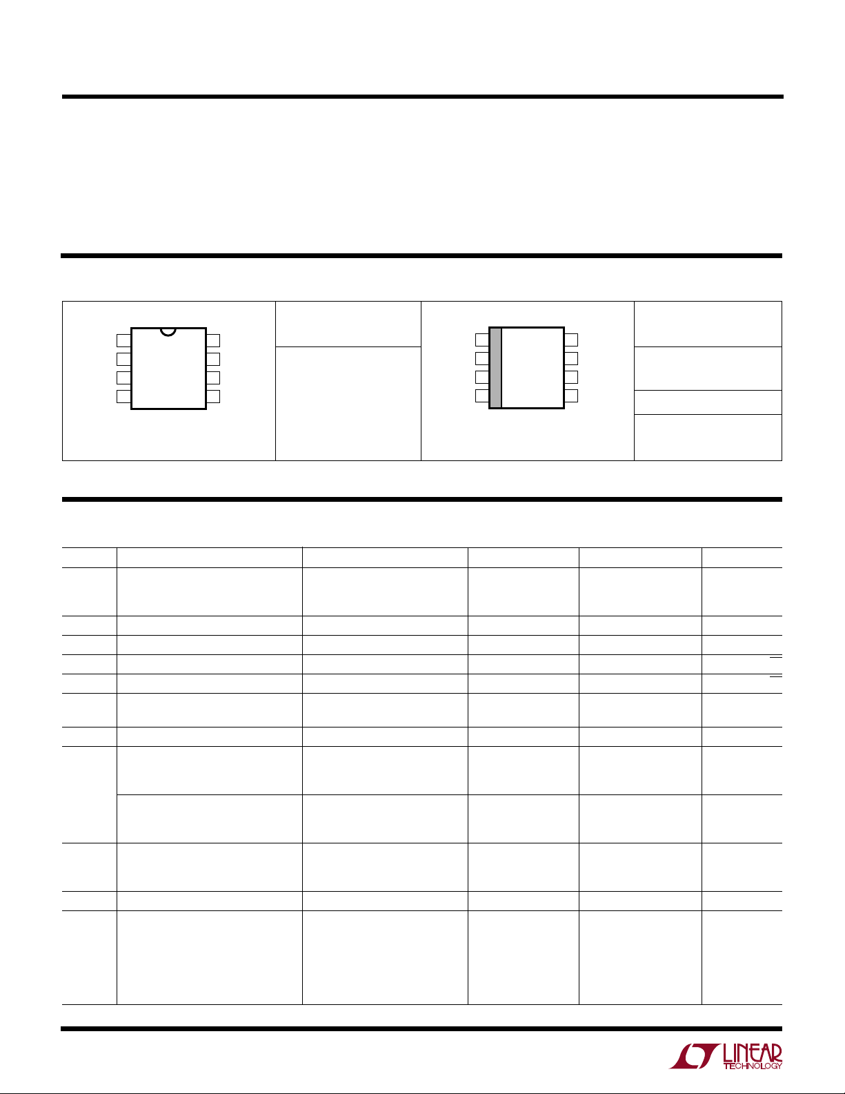
PACKAGE/ORDER INFORMATION
TOP VIEW
1NULL
2
–IN
+IN
3
–
V
N8 PACKAGE, 8-LEAD PLASTIC DIP
T
= 150°C, θJA = 130°C/ W
JMAX
Consult factory for Industrial and Military grade parts.
8
NULL
+
7
V
6
V
OUT
54
NC
ORDER PART
NUMBER
LT1357CN8
Specified Temperature Range (Note 6)... –40°C to 85°C
Maximum Junction Temperature (See Below)
S
Plastic Package ................................................150°C
Storage Temperature Range ................. –65°C to 150°C
Lead Temperature (Soldering, 10 sec).................. 300°C
U
TOP VIEW
1NULL
2
–IN
+IN
3
–
V
S8 PACKAGE, 8-LEAD PLASTIC SOIC
T
= 150°C, θJA = 190°C/ W
JMAX
8
NULL
7
V
6
V
54
NC
+
OUT
ORDER PART
NUMBER
LT1357CS8
S8 PART MARKING
1357
ELECTRICAL CHARACTERISTICS
SYMBOL PARAMETER CONDITIONS V
V
OS
I
OS
I
B
e
n
i
n
R
IN
C
IN
CMRR Common Mode Rejection Ratio V
PSRR Power Supply Rejection Ratio VS = ±2.5V to ±15V 92 106 dB
A
VOL
Input Offset Voltage ±15V 0.2 0.6 mV
Input Offset Current ±2.5V to ±15V 40 120 nA
Input Bias Current ±2.5V to ±15V 120 500 nA
Input Noise Voltage f = 10kHz ±2.5V to ±15V 8 nV/√Hz
Input Noise Current f = 10kHz ±2.5V to ±15V 0.8 pA/√Hz
Input Resistance V
Input Capacitance ±15V 3 pF
Input Voltage Range
Input Voltage Range
Large-Signal Voltage Gain V
+
–
= ±12V ±15V 35 80 MΩ
CM
Differential ±15V 6 MΩ
= ±12V ±15V 80 97 dB
CM
V
= ±2.5V ±5V 78 84 dB
CM
V
= ±0.5V ±2.5V 68 75 dB
CM
OUT
V
OUT
V
OUT
V
OUT
V
OUT
V
OUT
TA = 25°C, VCM = 0V unless otherwise noted.
SUPPLY
±5V 0.2 0.6 mV
±2.5V 0.3 0.8 mV
±15V 12.0 13.4 V
±5V 2.5 3.5 V
±2.5V 0.5 1.1 V
±15V –13.2 –12.0 V
±5V – 3.3 –2.5 V
±2.5V –0.9 – 0.5 V
= ±12V, RL = 1k ±15V 20.0 65 V/mV
= ±10V, RL = 500Ω±15V 7.0 25 V/mV
= ±2.5V, RL = 1k ±5V 20.0 45 V/mV
= ±2.5V, RL = 500Ω±5V 7.0 25 V/mV
= ±2.5V, RL = 150Ω±5V 1.5 6 V/mV
= ±1V, RL = 500Ω±2.5V 7.0 30 V/mV
MIN TYP MAX UNITS
2
LT1357
ELECTRICAL CHARACTERISTICS
SYMBOL PARAMETER CONDITIONS V
V
I
I
OUT
OUT
SC
Output Swing RL = 1k, V
RL = 500Ω, V
R
= 500Ω, V
L
RL = 150Ω, V
R
= 500Ω, V
L
Output Current V
Short-Circuit Current V
V
OUT
OUT
OUT
TA = 25°C, VCM = 0V unless otherwise noted.
SUPPLY
= ±40mV ±15V 13.3 13.8 ±V
IN
= ±40mV ±15V 12.0 12.8 ±V
IN
= ±40mV ±5V 3.5 4.0 ±V
IN
= ±40mV ±5V 2.5 3.3 ±V
IN
= ±40mV ±2.5V 1.3 1.7 ±V
IN
= ±12V ±15V 24.0 30 mA
= ±2.5V ±5V 16.7 25 mA
= 0V, V
= ±3V ±15V 30 42 mA
IN
MIN TYP MAX UNITS
SR Slew Rate AV = –2, (Note 3) ±15V 300 600 V/µs
±5V 150 220 V/µs
Full Power Bandwidth 10V Peak, (Note 4) ±15V 9.6 MHz
3V Peak, (Note 4) ±5V 11.7 MHz
GBW Gain Bandwidth f = 200kHz, RL = 2k ±15V 18 25 MHz
±5V 15 22 MHz
±2.5V 20 MHz
tr, t
f
Rise Time, Fall Time AV = 1, 10%-90%, 0.1V ±15V 8 ns
±5V 9 ns
Overshoot AV = 1, 0.1V ±15V 27 %
±5V 27 %
Propagation Delay 50% VIN to 50% V
, 0.1V ±15V 9 ns
OUT
±5V 11 ns
t
s
Settling Time 10V Step, 0.1%, AV = –1 ±15V 115 ns
10V Step, 0.01%, AV = –1 ±15V 220 ns
5V Step, 0.1%, A
= –1 ±5V 110 ns
V
5V Step, 0.01%, AV = –1 ±5V 380 ns
Differential Gain f = 3.58MHz, AV = 2, RL = 1k ±15V 0.1 %
±5V 0.1 %
Differential Phase f = 3.58MHz, AV = 2, RL = 1k ±15V 0.50 Deg
±5V 0.35 Deg
R
O
I
S
Output Resistance AV = 1, f = 100kHz ±15V 0.3 Ω
Supply Current ±15V 2.0 2.5 mA
±5V 1.9 2.4 mA
0°C ≤ TA ≤ 70°C, VCM = 0V unless otherwise noted.
SYMBOL PARAMETER CONDITIONS V
V
OS
Input Offset Voltage ±15V ● 0.8 mV
SUPPLY
±5V
±2.5V ● 1.0 mV
Input VOS Drift (Note 5) ±2.5V to ±15V ● 58 µV/°C
I
OS
I
B
CMRR Common Mode Rejection Ratio V
Input Offset Current ±2.5V to ±15V ● 180 nA
Input Bias Current ±2.5V to ±15V ● 750 nA
= ±12V ±15V ● 79 dB
CM
V
= ±2.5V ±5V ● 77 dB
CM
V
= ±0.5V ±2.5V ● 67 dB
CM
PSRR Power Supply Rejection Ratio VS = ±2.5V to ±15V ● 90 dB
A
VOL
Large-Signal Voltage Gain V
= ±12V, RL = 1k ±15V ● 15 V/mV
OUT
V
= ±10V, RL = 500Ω±15V ● 5 V/mV
OUT
V
= ±2.5V, RL = 1k ±5V ● 15 V/mV
OUT
V
= ±2.5V, RL = 500Ω±5V ● 5 V/mV
OUT
V
= ±2.5V, RL = 150Ω±5V ● 1 V/mV
OUT
V
= ±1V, RL = 500Ω±2.5V ● 5 V/mV
OUT
MIN TYP MAX UNITS
● 0.8 mV
3
LT1357
ELECTRICAL CHARACTERISTICS
SYMBOL PARAMETER CONDITIONS V
V
I
I
OUT
OUT
SC
Output Swing RL = 1k, V
= 500Ω, V
R
L
R
= 500Ω, V
L
= 150Ω, V
R
L
= 500Ω, V
R
L
Output Current V
Short-Circuit Current V
V
OUT
OUT
OUT
0°C ≤ TA ≤ 70°C, VCM = 0V unless otherwise noted.
SUPPLY
= ±40mV ±15V ● 13.2 ±V
IN
= ±40mV ±15V ● 11.5 ±V
IN
= ±40mV ±5V ● 3.4 ±V
IN
= ±40mV ±5V ● 2.3 ±V
IN
= ±40mV ±2.5V ● 1.2 ±V
IN
= ±11.5V ±15V ● 23.0 mA
= ±2.3V ±5V ● 15.3 mA
= 0V, V
= ±3V ±15V ● 25 mA
IN
MIN TYP MAX UNITS
SR Slew Rate AV = –2, (Note 3) ±15V ● 225 V/µs
±5V
● 125 V/µs
GBW Gain-Bandwidth f = 200kHz,RL = 2k ±15V ● 15 MHz
±5V
I
S
Supply Current ±15V ● 2.9 mA
● 12 MHz
±5V ● 2.8 mA
–40°C ≤ TA ≤ 85°C, VCM = 0V unless otherwise noted. (Note 6)
SYMBOL PARAMETER CONDITIONS V
V
OS
Input Offset Voltage ±15V ● 1.3 mV
SUPPLY
±5V
±2.5V
Input VOS Drift (Note 5) ±2.5V to ±15V ● 58 µV/°C
I
OS
I
B
CMRR Common Mode Rejection Ratio V
Input Offset Current ±2.5V to ±15V ● 300 nA
Input Bias Current ±2.5V to ±15V ● 900 nA
= ±12V ±15V ● 78 dB
CM
= ±2.5V ±5V ● 76 dB
V
CM
V
= ±0.5V ±2.5V ● 66 dB
CM
PSRR Power Supply Rejection Ratio VS = ±2.5V to ±15V ● 90 dB
A
V
I
I
VOL
OUT
OUT
SC
Large-Signal Voltage Gain V
= ±12V, RL = 1k ±15V ● 10.0 V/mV
OUT
= ±10V, RL = 500Ω±15V ● 2.5 V/mV
V
OUT
= ±2.5V, RL = 1k ±5V ● 10.0 V/mV
V
OUT
V
= ±2.5V, RL = 500Ω±5V ● 2.5 V/mV
OUT
= ±2.5V, RL = 150Ω±5V ● 0.6 V/mV
V
OUT
= ±1V, RL = 500Ω±2.5V ● 2.5 V/mV
V
OUT
Output Swing RL = 1k, V
= 500Ω, V
R
L
= 500Ω, V
R
L
R
= 150Ω, V
L
= 500Ω, V
R
L
Output Current V
Short-Circuit Current V
= ±11V ±15V ● 22 mA
OUT
= ±2.1V ±5V ● 14 mA
V
OUT
= 0V, V
OUT
= ±40mV ±15V ● 13.0 ±V
IN
= ±40mV ±15V ● 11.0 ±V
IN
= ±40mV ±5V ● 3.4 ±V
IN
= ±40mV ±5V ● 2.1 ±V
IN
= ±40mV ±2.5V ● 1.2 ±V
IN
= ±3V ±15V ● 24 mA
IN
SR Slew Rate AV = –2, (Note 3) ±15V ● 180 V/µs
±5V ● 100 V/µs
GBW Gain-Bandwith f = 200kHz, R
= 2k ±15V ● 14 MHz
L
±5V ● 11 MHz
I
S
Supply Current ±15V ● 3.0 mA
±5V ● 2.9 mA
MIN TYP MAX UNITS
● 1.3 mV
● 1.5 mV
4
 Loading...