

Linear Technology LT1351 Datasheet
FEATURES
■
3MHz Gain Bandwidth
■
200V/µs Slew Rate
■
250µA Supply Current
■
Available in Tiny MSOP Package
■
C-LoadTM Op Amp Drives All Capacitive Loads
■
Unity-Gain Stable
■
Power Saving Shutdown Feature
■
Maximum Input Offset Voltage: 600µV
■
Maximum Input Bias Current: 50nA
■
Maximum Input Offset Current: 15nA
■
Minimum DC Gain, RL = 2k: 30V/mV
■
Input Noise Voltage: 14nV/√Hz
■
Settling Time to 0.1%, 10V Step: 700ns
■
Settling Time to 0.01%, 10V Step: 1.25µs
■
Minimum Output Swing into 1k: ±13V
■
Minimum Output Swing into 500Ω: ±3.4V
■
Specified at ±2.5V, ±5V and ±15V
U
APPLICATIONS
■
Battery-Powered Systems
■
Wideband Amplifiers
■
Buffers
■
Active Filters
■
Data Acquisition Systems
■
Photodiode Amplifiers
LT1351
250µA, 3MHz, 200V/µs
Operational Amplifier
U
DESCRIPTION
The LT®1351 is a low power, high speed, high slew rate
operational amplifier with outstanding AC and DC performance. The LT1351 features lower supply current, lower
input offset voltage, lower input bias current and higher
DC gain than devices with comparable bandwidth. The
circuit combines the slewing performance of a current
feedback amplifier in a true operational amplifier with
matched high impedance inputs. The high slew rate ensures that the large-signal bandwidth is not degraded. The
amplifier is a single gain stage with outstanding settling
characteristics which make the circuit an ideal choice for
data acquisition systems. The output drives a 1kΩ load to
±13V with ± 15V supplies and a 500Ω load to ±3.4V on ±5V
supplies. The amplifier is also stable with any capacitive
load which makes it useful in buffer or cable driver
applications.
The LT1351 is a member of a family of fast, high performance amplifiers using this unique topology and employing Linear Technology Corporation’s advanced
complementary bipolar processing. For dual and quad
amplifier versions of the LT1351 see the LT1352/LT1353
data sheet. For higher bandwidth devices with higher
supply current see the LT1354 through LT1365 data sheets.
Singles, duals and quads of each amplifier are available.
, LTC and LT are registered trademarks of Linear Technology Corporation.
C-Load is a trademark of Linear Technology Corporation.
U
TYPICAL APPLICATION
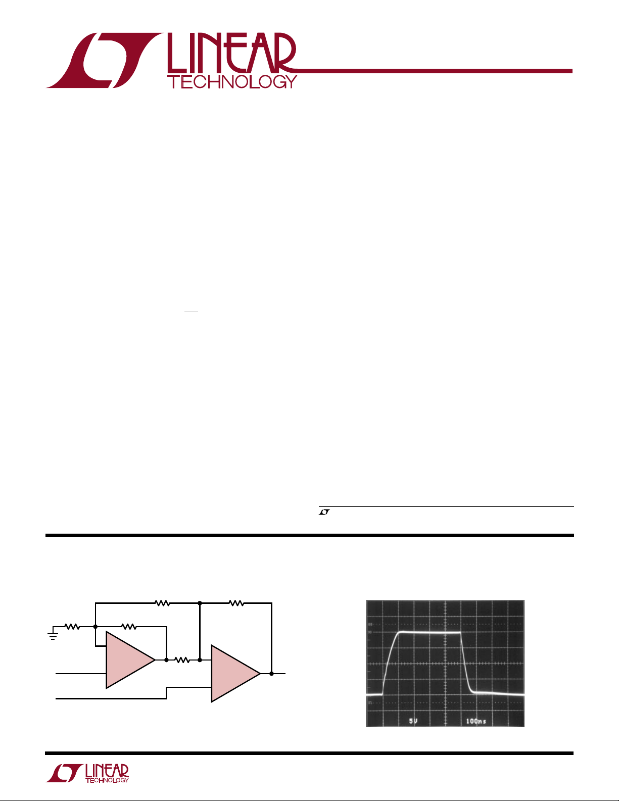
Instrumentation Amplifier
R1
50k
–
V
IN
+
GAIN = [R4/R3][1 + (1/2)(R2/R1 + R3/R4) + (R2 + R3)/R5] = 102
TRIM R5 FOR GAIN
TRIM R1 FOR COMMON MODE REJECTION
BW = 30kHz
–
LT1351
+
R2
5k
R5
1.1k
R3
5k
–
+
50k
LT1351
Large-Signal Response
R4
V
OUT
1351 TA01
AV = –1 1351 TA02
1
LT1351
1
2
3
4
8
7
6
5
TOP VIEW
NULL
–IN
+IN
V
–
NULL
V
+
V
OUT
SHDN
N8 PACKAGE
8-LEAD PDIP
S8 PACKAGE
8-LEAD PLASTIC SO
WW
W
U
ABSOLUTE MAXIMUM RATINGS
Total Supply Voltage (V+ to V–) .............................. 36V
Differential Input Voltage (Transient Only, Note 1)...
±10V
Input Voltage .......................................................... ±V
Output Short-Circuit Duration (Note 2) ........... Indefinite
Operating Temperature Range ................ –40°C to 85°C
U
W
PACKAGE/ORDER INFORMATION
TOP VIEW
NULL
1
–IN
2
+IN
3
–
V
4
MS8 PACKAGE
8-LEAD PLASTIC MSOP
T
= 150°C, θJA = 250°C/ W
JMAX
Consult factory for Industrial and Military grade parts.
8
7
6
5
NULL
+
V
V
OUT
SHDN
ORDER PART
NUMBER
LT1351CMS8
MS8 PART MARKING
LTBT
Specified Temperature Range (Note 6) .....
–40°C to 85°C
Maximum Junction Temperature (See Below)
S
Plastic Package ................................................ 150°C
Storage Temperature Range ................. –65°C to 150°C
Lead Temperature (Soldering, 10 sec).................. 300°C
U
ORDER PART
NUMBER
LT1351CN8
LT1351CS8
S8 PART MARKING
T
= 150°C, θJA = 130°C/ W (N8)
JMAX
T
= 150°C, θJA = 190°C/ W (S)
JMAX
1351
ELECTRICAL CHARACTERISTICS
SYMBOL PARAMETER CONDITIONS V
V
OS
I
OS
I
B
e
n
i
n
R
IN
C
IN
CMRR Common Mode Rejection Ratio VCM = ±12V ±15V 80 94 dB
PSRR Power Supply Rejection Ratio VS = ±2.5V to ±15V 90 106 dB
2
Input Offset Voltage ±15V 0.2 0.6 mV
Input Offset Current ±2.5V to ±15V 5 15 nA
Input Bias Current ±2.5V to ±15V 20 50 nA
Input Noise Voltage f = 10kHz ±2.5V to ±15V 14 nV/√Hz
Input Noise Current f = 10kHz ±2.5V to ±15V 0.5 pA/√Hz
Input Resistance VCM = ±12V ±15V 300 600 MΩ
Differential ±15V 20 MΩ
Input Capacitance ±15V 3 pF
Positive Input Voltage Range ±15V 12.0 13.5 V
Negative Input Voltage Range ±15V –13.5 –12.0 V
VCM = ±2.5V ±5V 78 86 dB
V
TA = 25°C, VCM = 0V unless otherwise noted.
SUPPLY
±5V 0.2 0.6 mV
±2.5V 0.3 0.8 mV
±5V 2.5 3.5 V
±2.5V 0.5 1.0 V
±5V –3.5 –2.5 V
±2.5V –1.0 –0.5 V
= ±0.5V ±2.5V 68 77 dB
CM
MIN TYP MAX UNITS
LT1351
ELECTRICAL CHARACTERISTICS
SYMBOL PARAMETER CONDITIONS V
A
VOL
V
OUT
Large-Signal Voltage Gain V
OUT
V
OUT
V
OUT
V
OUT
V
OUT
V
OUT
V
OUT
Output Swing RL = 5k, VIN = ±10mV ±15V 13.5 14.0 ±V
= 2k, VIN = ±10mV ±15V 13.4 13.8 ±V
R
L
TA = 25°C, VCM = 0V unless otherwise noted.
SUPPLY
= ±12V, RL = 5k ±15V 40 80 V/mV
= ±10V, RL = 2k ±15V 30 60 V/mV
= ±10V, RL = 1k ±15V 20 40 V/mV
= ±2.5V, RL = 5k ±5V 30 60 V/mV
= ±2.5V, RL = 2k ±5V 25 50 V/mV
= ±2.5V, RL = 1k ±5V 15 30 V/mV
= ±1V, RL = 5k ±2.5V 20 40 V/mV
MIN TYP MAX UNITS
RL = 1k, VIN = ±10mV ±15V 13.0 13.4 ±V
= 1k, VIN = ±10mV ±5V 3.5 4.0 ±V
R
L
= 500Ω, VIN = ±10mV ±5V 3.4 3.8 ±V
R
L
= 5k, VIN = ±10mV ±2.5V 1.3 1.7 ±V
R
L
I
OUT
I
SC
Output Current V
Short-Circuit Current V
= ±13V ±15V 13.0 13.4 mA
OUT
= ±3.4V ±5V 6.8 7.6 mA
V
OUT
= 0V, VIN = ±3V ±15V 30 45 mA
OUT
SR Slew Rate AV = –1, RL = 5k (Note 3) ±15V 120 200 V/µs
±5V 30 50 V/µs
Full-Power Bandwidth 10V Peak (Note 4) ±15V 3.2 MHz
3V Peak (Note 4) ±5V 2.6 MHz
GBW Gain Bandwidth f = 200kHz, RL = 10k ±15V 2.0 3.0 MHz
±5V 1.8 2.7 MHz
±2.5V 2.5 MHz
tr, t
f
Rise Time, Fall Time AV = 1, 10% to 90%, 0.1V ±15V 46 ns
±5V 53 ns
Overshoot AV = 1, 0.1V ±15V 13 %
±5V 16 %
Propagation Delay 50% VIN to 50% V
, 0.1V ±15V 41 ns
OUT
±5V 52 ns
t
s
Settling Time 10V Step, 0.1%, AV = –1 ±15V 700 ns
10V Step, 0.01%, A
5V Step, 0.1%, A
= –1 ±15V 1250 ns
V
= –1 ±5V 950 ns
V
5V Step, 0.01%, AV = –1 ±5V 1400 ns
R
O
I
SHDN
I
S
Output Resistance AV = 1, f = 20kHz ±15V 1.5 Ω
Shutdown Input Current SHDN = VEE + 0.1V ±15V – 10 µA
SHDN = V
CC
±15V 0.1 2 µA
Supply Current ±15V 250 330 µA
±5V 220 300 µA
SHDN = V
+ 0.1V ±5V 10 µA
EE
0°C ≤ TA ≤ 70°C, VCM = 0V unless otherwise noted.
SYMBOL PARAMETER CONDITIONS V
V
OS
I
OS
I
B
Input Offset Voltage ±15V 0.8 mV
Input VOS Drift (Note 5) ±2.5V to ±15V 3 8 µV/°C
Input Offset Current ±2.5V to ±15V 20 nA
Input Bias Current ±2.5V to ±15V 75 nA
SUPPLY
MIN TYP MAX UNITS
±5V 0.8 mV
±2.5V 1.0 mV
3
LT1351
ELECTRICAL CHARACTERISTICS
SYMBOL PARAMETER CONDITIONS V
0°C ≤ TA ≤ 70°C, VCM = 0V unless otherwise noted.
SUPPLY
MIN TYP MAX UNITS
CMRR Common Mode Rejection Ratio VCM = ±12V ±15V 78 dB
= ±2.5V ±5V 77 dB
V
CM
= ±0.5V ±2.5V 67 dB
V
CM
PSRR Power Supply Rejection Ratio VS = ±2.5V to ±15V 89 dB
A
VOL
V
OUT
Large-Signal Voltage Gain V
= ±12V, RL = 5k ±15V 25 V/mV
OUT
= ±10V, RL = 2k ±15V 20 V/mV
V
OUT
= ±2.5V, RL = 5k ±5V 20 V/mV
V
OUT
V
= ±2.5V, RL = 2k ±5V 15 V/mV
OUT
= ±2.5V, RL = 1k ±5V 10 V/mV
V
OUT
= ±1V, RL = 5k ±2.5V 15 V/mV
V
OUT
Output Swing RL = 5k, VIN = ±10mV ±15V 13.4 ±V
= 2k, VIN = ±10mV ±15V 13.3 ±V
R
L
= 1k, VIN = ±10mV ±15V 12.0 ±V
R
L
= 1k, VIN = ±10mV ±5V 3.4 ±V
R
L
RL= 500Ω, VIN = ±10mV ±5V 3.3 ±V
= 5k, VIN = ±10mV ±2.5V 1.2 ±V
R
L
I
I
OUT
SC
Output Current V
Short-Circuit Current V
= ±12V ±15V 12.0 mA
OUT
= ±3.3V ±5V 6.6 mA
V
OUT
= 0V, VIN = ±3V ±15V 24 mA
OUT
SR Slew Rate AV = –1, RL = 5k (Note 3) ±15V 100 V/µs
±5V 21 V/µs
GBW Gain Bandwidth f = 200kHz, RL = 10k ±15V 1.8 MHz
±5V 1.6 MHz
I
SHDN
I
S
Shutdown Input Current SHDN = VEE + 0.1V ±15V – 20 µA
SHDN = V
CC
±15V 3 µA
Supply Current ±15V 380 µA
±5V 355 µA
SHDN = V
+ 0.1V ±5V 20 µA
EE
–40°C ≤ TA ≤ 85°C, VCM = 0V unless otherwise noted (Note 6).
SYMBOL PARAMETER CONDITIONS V
V
OS
Input Offset Voltage ±15V 1.0 mV
SUPPLY
±5V 1.0 mV
±2.5V 1.2 mV
Input VOS Drift (Note 5) ±2.5V to ±15V 3 8 µV/°C
I
OS
I
B
Input Offset Current ±2.5V to ±15V 30 nA
Input Bias Current ±2.5V to ±15V 100 nA
CMRR Common Mode Rejection Ratio VCM = ±12V ±15V 76 dB
= ±2.5V ±5V 76 dB
V
CM
= ±0.5V ±2.5V 66 dB
V
CM
PSRR Power Supply Rejection Ratio VS = ±2.5V to ±15V 87 dB
A
VOL
Large-Signal Voltage Gain V
= ±12V, RL = 5k ±15V 20 V/mV
OUT
= ±10V, RL = 2k ±15V 15 V/mV
V
OUT
= ±2.5V, RL = 5k ±5V 15 V/mV
V
OUT
= ±2 .5V, RL = 2k ±5V 10 V/mV
V
OUT
V
= ±2.5V, RL = 1k ±5V 8 V/mV
OUT
= ±1V, RL = 5k ±2.5V 10 V/mV
V
OUT
MIN TYP MAX UNITS
4
LT1351
ELECTRICAL CHARACTERISTICS
SYMBOL PARAMETER CONDITIONS V
V
OUT
Output Swing RL = 5k, VIN = ±10mV ±15V 13.3 ±V
R
L
R
L
R
L
–40°C ≤ TA ≤ 85°C, VCM = 0V unless otherwise noted (Note 6).
SUPPLY
= 2k, VIN = ±10mV ±15V 13.2 ±V
= 1k, VIN = ±10mV ±15V 10.0 ±V
= 1k, VIN = ±10mV ±5V 3.3 ±V
MIN TYP MAX UNITS
RL= 500Ω, VIN = ±10mV ±5V 3.2 ±V
= 5k, VIN = ±10mV ±2.5V 1.1 ±V
R
L
I
OUT
I
SC
Output Current V
Short-Circuit Current V
= ±10V ±15V 10.0 mA
OUT
= ±3.2V ±5V 6.4 mA
V
OUT
= 0V, VIN = ±3V ±15V 20 mA
OUT
SR Slew Rate AV = –1, RL = 5k (Note 3) ±15V 50 V/µs
±5V 15 V/µs
GBW Gain Bandwidth f = 200kHz, RL = 10k ±15V 1.6 MHz
±5V 1.4 MHz
I
SHDN
I
S
Shutdown Input Current SHDN = VEE + 0.1V ±15V – 30 µA
SHDN = V
CC
±15V 5 µA
Supply Current ±15V 390 µA
±5V 380 µA
SHDN = V
Note 1: Differential inputs of ±10V are appropriate for transient operation
only, such as during slewing. Large, sustained differential inputs will cause
excessive power dissipation and may damage the part. See Input
Considerations in the Applications Information section of this data sheet
for more details.
Note 2: A heat sink may be required to keep the junction temperature
+ 0.1V ±5V 30 µA
EE
Note 4: Full-power bandwidth is calculated from the slew rate
measurement: FPBW = (Slew Rate)/2πV
.
P
Note 5: This parameter is not 100% tested.
Note 6: The LT1351 is designed, characterized and expected to meet these
extended temperature limits, but is not tested at –40°C and at 85°C.
Guaranteed I grade parts are available; consult factory.
below absolute maximum when the output is shorted indefinitely.
Note 3: Slew rate is measured between ±8V on the output with ±12V
input for ±15V supplies and ±2V on the output with ±3V input for ±5V
supplies.
W
U
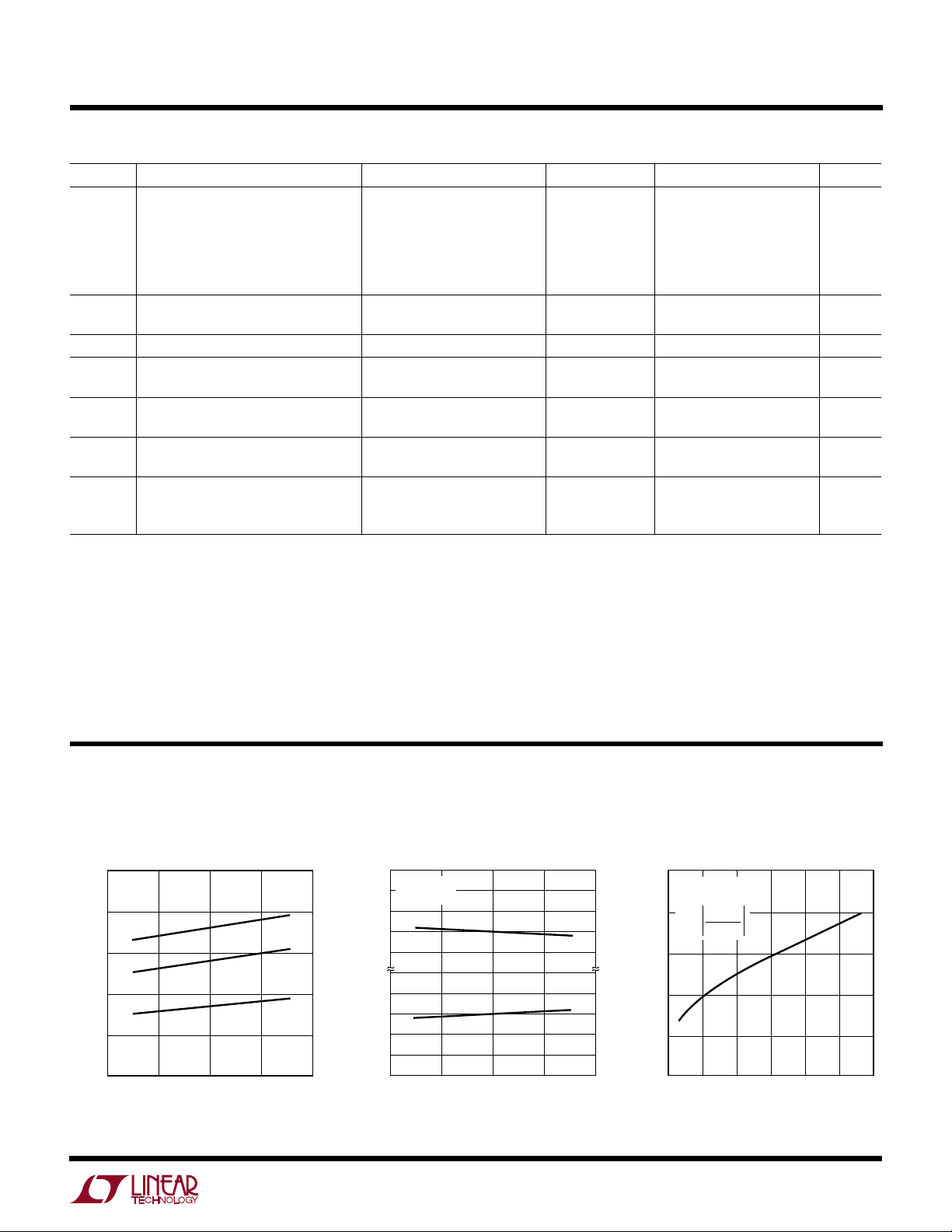
TYPICAL PERFORMANCE CHARACTERISTICS
Supply Current vs Supply Voltage
and Temperature
350
300
125°C
250
25°C
200
–55°C
SUPPLY CURRENT (µA)
150
100
0
5
10
SUPPLY VOLTAGE (±V)
15
20
1351 G01
Input Common Mode Range
vs Supply Voltage
+
V
TA = 25°C
–0.5
–1.0
–1.5
–2.0
2.0
1.5
COMMON MODE RANGE (V)
1.0
0.5
V
= 1mV
∆V
OS
–
0
5
10
SUPPLY VOLTAGE (±V)
15
1351 G02
Input Bias Current
vs Input Common Mode Voltage
30
TA = 25°C
= ±15V
V
S
+
–10
+ I
I
B
2
–
B
–5 0 5
10 15
1351 G03
20
IB =
10
0
INPUT BIAS CURRENT (nA)
–10
–20
20
–15
INPUT COMMON MODE VOLTAGE (V)
5
 Loading...