

Linear Technology LT1207 Datasheet
LT1207
Dual 250mA/60MHz
Current Feedback Amplifier
EATU
F
■
250mA Minimum Output Drive Current
■
60MHz Bandwidth, AV = 2, RL = 100Ω
■
900V/µs Slew Rate, AV = 2, RL = 50Ω
■
0.02% Differential Gain, AV = 2, RL = 30Ω
■
0.17° Differential Phase, AV = 2, RL = 30Ω
■
High Input Impedance: 10MΩ
■
Shutdown Mode: IS < 200µA per Amplifier
■
Stable with CL = 10,000pF
RE
S
U
APPLICATIO S
■
ADSL/HDSL Drivers
■
Video Amplifiers
■
Cable Drivers
■
RGB Amplifiers
■
Test Equipment Amplifiers
■
Buffers
DUESCRIPTIO
The LT®1207 is a dual version of the LT1206 high speed
current feedback amplifier. Like the LT1206, each CFA in
the dual has excellent video characteristics: 60MHz bandwidth, 250mA minimum output drive current, 400V/µs
minimum slew rate, low differential gain (0.02% typ) and
low differential phase (0.17° typ). The LT1207 includes a
pin for an optional compensation network which stabilizes the amplifier for heavy capacitive loads. Both amplifiers have thermal and current limit circuits which protect
against fault conditions. These capabilities make the LT1207
well suited for driving difficult loads such as cables in video
or digital communication systems.
Operation is fully specified from ±5V to ±15V supplies.
Supply current is typically 20mA per amplifier. Two
micropower shutdown controls place each amplifier in a
high impedance low current mode, dropping supply
current to 200µA per amplifier. For reduced bandwidth
applications, supply current can be lowered by adding a
resistor in series with the Shutdown pin.
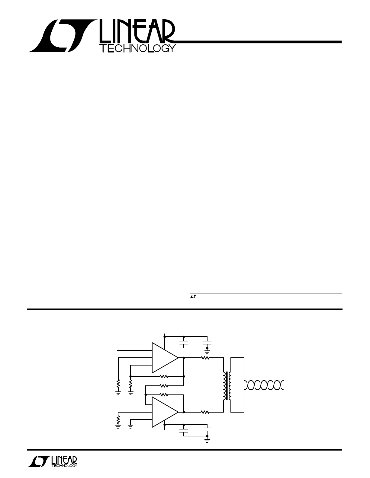
TYPICAL APPLICATION
V
IN
15k
15k
U
SHDN A
240Ω
SHDN B
5V
+
1/2 LT1207
–
720Ω
720Ω
720Ω
–
1/2 LT1207
+
–5V
The LT1207 is manufactured on Linear Technology's
complementary bipolar process and is available in a low
thermal resistance 16-lead SO package.
, LTC and LT are registered trademarks of Linear Technology Corporation.
HDSL Driver
0.1µF*
0.1µF*
62Ω
62Ω
+
2.2µF**
2.2µF**
+
L1
*
CERAMIC
**
TANTALUM
L1 =TRANSPOWER SMPT–308
OR SIMILAR DEVICE
1207 • TA01
1
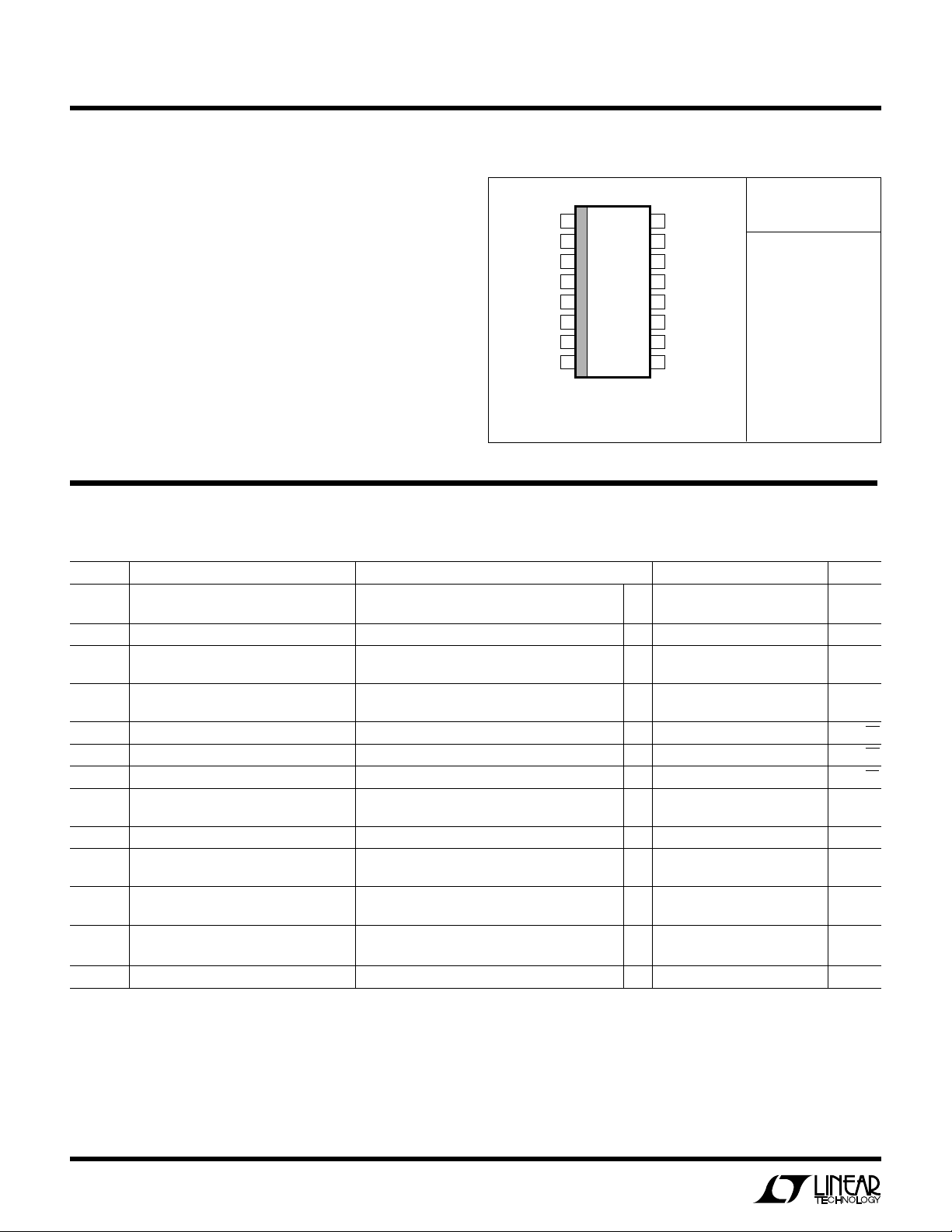
LT1207
WU
U
PACKAGE
/
O
RDER I FOR ATIO
TOP VIEW
S PACKAGE
16-LEAD PLASTIC SO
1
2
3
4
5
6
7
8
16
15
14
13
12
11
10
9
V+
–IN A
+IN A
SHDN A
–IN B
+IN B
SHDN B
V
+
V+
OUT A
V
–
A
COMP A
OUT B
V
–
B
COMP B
V
+
W
O
A
LUTEXI T
S
Supply Voltage ..................................................... ±18V
Input Current per Amplifier ............................... ±15mA
A
WUW
ARB
U
G
I
S
ORDER PART
NUMBER
Output Short-Circuit Duration (Note 1)....... Continuous
Specified Temperature Range (Note 2)...... 0°C to 70°C
LT1207CS
Operating Temperature Range ............... –40°C to 85°C
Junction Temperature......................................... 150°C
Storage Temperature Range ................. –65°C to 150°C
Lead Temperature (Soldering, 10 sec)................. 300°C
θJA = 40°C/W (NOTE 3)
Consult factory for Industrial and Military grade parts.
ELECTRICAL CHARACTERISTICS
VCM = 0, ±5V ≤ VS ≤ ±15V, pulse tested, V
SYMBOL PARAMETER CONDITIONS MIN TYP MAX UNITS
V
OS
+
I
IN
–
I
IN
e
n
+i
n
–i
n
R
IN
C
IN
CMRR Common Mode Rejection Ratio VS = ±15V, VCM = ±12V ● 55 62 dB
PSRR Power Supply Rejection Ratio VS = ±5V to ±15V ● 60 77 dB
Input Offset Voltage TA = 25°C ±3 ±10 mV
Input Offset Voltage Drift ● 10 µV/°C
Noninverting Input Current TA = 25°C ±2 ±5 µA
Inverting Input Current TA = 25°C ±10 ±60 µA
Input Noise Voltage Density f = 10kHz, RF = 1k, RG = 10Ω, RS = 0Ω 3.6 nV/√Hz
Input Noise Current Density f = 10kHz, RF = 1k, RG = 10Ω, RS = 10k 2 pA/√Hz
Input Noise Current Density f = 10kHz, RF = 1k, RG = 10Ω, RS = 10k 30 pA/√Hz
Input Resistance VIN = ±12V, VS = ±15V ● 1.5 10 MΩ
Input Capacitance VS = ±15V 2 pF
Input Voltage Range VS = ±15V ● ±12 ±13.5 V
Inverting Input Current VS = ±15V, VCM = ±12V ● 0.1 10 µA/V
Common Mode Rejection V
= 0V, V
SHDN A
VIN = ±2V, VS = ±5V ● 0.5 5 MΩ
VS = ±5V ● ±2 ±3.5 V
V
= ±5V, VCM = ±2V ● 50 60 dB
S
= ±5V, VCM = ±2V ● 0.1 10 µA/V
S
= 0V, unless otherwise noted.
SHDN B
● ±15 mV
● ±20 µA
● ±100 µA
2
LT1207
ELECTRICAL CHARACTERISTICS
VCM = 0, ±5V ≤ VS ≤ ±15V, pulse tested, V
SYMBOL PARAMETER CONDITIONS MIN TYP MAX UNITS
Noninverting Input Current VS = ±5V to ±15V ● 30 500 nA/V
Power Supply Rejection
Inverting Input Current VS = ±5V to ±15V ● 0.7 5 µA/V
Power Supply Rejection
A
V
R
OL
V
OUT
I
OUT
I
S
SR Slew Rate (Note 5) AV = 2, TA = 25°C 400 900 V/µs
BW Small-Signal Bandwidth VS = ±15V, Peaking ≤ 0.5dB 60 MHz
Large-Signal Voltage Gain VS = ±15V, V
Transresistance, ∆V
OUT
/∆I
–
IN
Maximum Output Voltage Swing VS = ±15V, RL = 50Ω, TA = 25°C ±11.5 ±12.5 V
Maximum Output Current RL = 1Ω ● 250 500 1200 mA
Supply Current per Amplifier VS = ±15V, V
Supply Current per Amplifier, VS = ±15V, TA = 25°C1217mA
R
= 51k (Note 4)
SHDN
Positive Supply Current VS = ±15V, V
per Amplifier, Shutdown
Output Leakage Current, Shutdown VS = ±15V, V
Differential Gain (Note 6) VS = ±15V, RF = 560Ω, RG = 560Ω, RL = 30Ω 0.02 %
Differential Phase (Note 6) VS = ±15V, RF = 560Ω, RG = 560Ω, RL = 30Ω 0.17 DEG
SHDN A
= 0V, V
VS = ±5V, V
VS = ±15V, V
V
= ±5V, V
S
V
= ±5V, RL = 25Ω, TA = 25°C ±2.5 ±3.0 V
S
= 0V, unless otherwise noted.
SHDN B
= ±10V, RL = 50Ω ● 55 71 dB
OUT
= ±2V, RL = 25Ω ● 55 68 dB
OUT
= ±10V, RL = 50Ω ● 100 260 kΩ
OUT
= ±2V, RL = 25Ω ● 75 200 kΩ
OUT
● ±10.0 V
● ±2.0 V
= 0V, TA = 25°C2030mA
SHDN
SHDN A
SHDN
= 15V, V
= 15V, V
= 15V ● 200 µA
SHDN B
= 0V ● 10 µA
OUT
●35 mA
RF = RG = 620Ω, RL = 100Ω
VS = ±15V, Peaking ≤ 0.5dB 52 MHz
R
= RG = 649Ω, RL = 50Ω
F
VS = ±15V, Peaking ≤ 0.5dB 43 MHz
RF = RG = 698Ω, RL = 30Ω
VS = ±15V, Peaking ≤ 0.5dB 27 MHz
R
= RG = 825Ω, RL = 10Ω
F
● denotes specifications which apply for 0°C ≤ T
The
≤ 70°C.
A
Note 1: Applies to short circuits to ground only. A short circuit between
the output and either supply may permanently damage the part when
operated on supplies greater than ±10V.
Note 2: Commercial grade parts are designed to operate over the
temperature range of –40°C to 85°C but are neither tested nor guaranteed
beyond 0°C to 70°C. Industrial grade parts tested over –40°C to 85°C are
available on special request. Consult factory.
Note 3: Thermal resistance θ
varies from 40°C/W to 60°C/W depending
JA
upon the amount of PC board metal attached to the device. θJA is specified
for a 2500mm2 test board covered with 2oz copper on both sides.
Note 4: R
is connected between the Shutdown pin and ground.
SHDN
Note 5: Slew rate is measured at ±5V on a ±10V output signal while
operating on ±15V supplies with R
= 1.5k, RG = 1.5k and RL = 400Ω.
F
Note 6: NTSC composite video with an output level of 2V.
3
LT1207
WU
U
S ALL-SIG AL BA DWIDTH
I
= 20mA per Amplifier Typical, Peaking ≤ 0.1dB
S
A
VS = ±5V, R
–1 150 562 562 48 21.4
10 150 442 48.7 40 19.2
R
V
SHDN
30 649 649 34 17
10 732 732 22 12.5
1 150 619 – 54 22.3
30 715 – 36 17.5
10 806 – 22.4 11.5
2 150 576 576 48 20.7
30 649 649 35 18.1
10 750 750 22.4 11.7
30 511 56.2 31 16.5
10 649 71.5 20 10.2
L
= 0Ω
R
R
F
G
IS = 10mA per Amplifier Typical, Peaking ≤ 0.1dB
A
VS = ±5V, R
–1 150 576 576 35 17
10 150 301 33.2 31 15.6
R
V
SHDN
30 681 681 25 12.5
10 750 750 16.4 8.7
1 150 665 – 37 17.5
30 768 – 25 12.6
10 845 – 16.5 8.2
2 150 590 590 35 16.8
30 681 681 25 13.4
10 768 768 16.2 8.1
30 392 43.2 23 11.9
10 499 54.9 15 7.8
L
= 10.2k
R
R
F
G
–3dB BW –0.1dB BW
(MHz) (MHz)
–3dB BW –0.1dB BW
(MHz) (MHz)
A
VS = ±15V, R
–1 150 681 681 50 19.2
1 150 768 – 66 22.4
2 150 665 665 55 23
10 150 487 536 44 20.7
A
VS = ±15V, R
–1 150 634 634 41 19.1
1 150 768 – 44 18.8
2 150 649 649 40 18.5
10 150 301 33.2 33 15.6
R
V
SHDN
30 768 768 35 17
10 887 887 24 12.3
30 909 – 37 17.5
10 1k – 23 12
30 787 787 36 18.5
10 931 931 22.5 11.8
30 590 64.9 33 17.5
10 768 84.5 20.7 10.8
R
V
SHDN
30 768 768 26.5 14
10 866 866 17 9.4
30 909 – 28 14.4
10 1k – 16.8 8.3
30 787 787 27 14.1
10 931 931 16.5 8.1
30 402 44.2 25 13.3
10 590 64.9 15.3 7.4
L
L
R
F
= 0Ω
R
F
= 60.4k
R
G
R
G
–3dB BW –0.1dB BW
(MHz) (MHz)
–3dB BW –0.1dB BW
(MHz) (MHz)
IS = 5mA per Amplifier Typical, Peaking ≤ 0.1dB
A
VS = ±5V, R
–1 150 604 604 21 10.5
10 150 100 11.1 16.2 5.8
R
V
SHDN
30 715 715 14.6 7.4
10 681 681 10.5 6.0
1 150 768 – 20 9.6
2 150 634 634 20 9.6
30 866 – 14.1 6.7
10 825 – 9.8 5.1
30 750 750 14.1 7.2
10 732 732 9.6 5.1
30 100 11.1 13.4 7.0
10 100 11.1 9.5 4.7
L
= 22.1k
R
F
R
G
–3dB BW –0.1dB BW
(MHz) (MHz)
4
A
VS = ±15V, R
–1 150 619 619 25 12.5
10 150 100 11.1 15.9 4.5
R
V
SHDN
30 787 787 15.8 8.5
10 825 825 10.5 5.4
1 150 845 – 23 10.6
30 1k – 15.3 7.6
10 1k – 10 5.2
2 150 681 681 23 10.2
30 845 845 15 7.7
10 866 866 10 5.4
30 100 11.1 13.6 6
10 100 11.1 9.6 4.5
L
R
= 121k
F
R
G
–3dB BW –0.1dB BW
(MHz) (MHz)
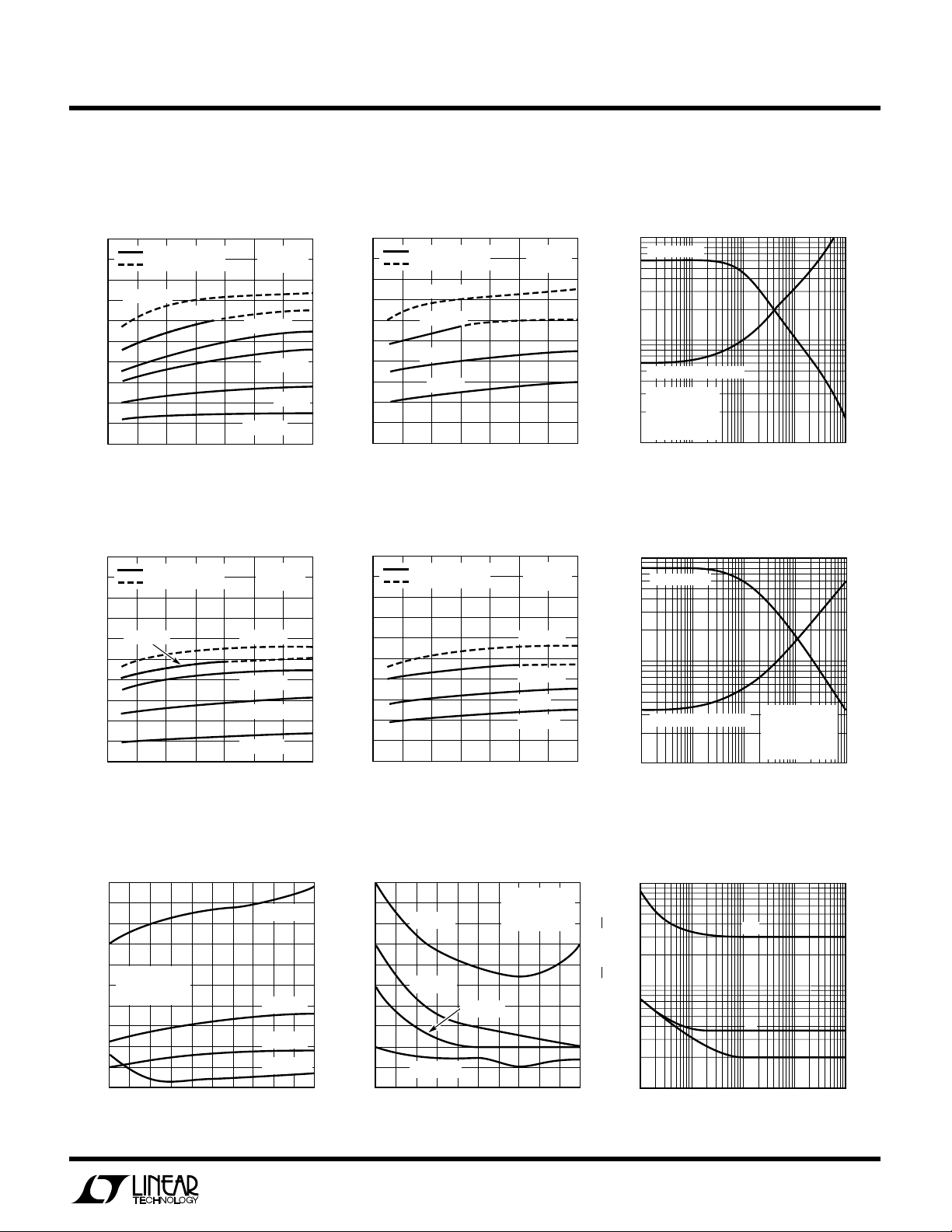
WU
CAPACITIVE LOAD (pF)
1
100
FEEDBACK RESISTOR (Ω)
1k
10k
100 10000
LT1207 • TPC03
10 1000
BANDWIDTH
FEEDBACK RESISTOR
A
V
= 2
R
L
= ∞
V
S
= ±15V
C
COMP
= 0.01µF
1
10
100
–3dB BANDWIDTH (MHz)
TYPICAL PERFOR A CE CHARACTERISTICS
Bandwidth vs Supply Voltage
100
90
80
70
60
50
40
30
–3dB BANDWIDTH (MHz)
20
10
0
PEAKING ≤ 0.5dB
PEAKING ≤ 5dB
RF = 470Ω
RF = 560Ω
4
610
8
SUPPLY VOLTAGE (±V)
12
Bandwidth vs Supply Voltage
100
90
80
70
60
50
40
30
–3dB BANDWIDTH (MHz)
20
10
0
PEAKING ≤ 0.5dB
PEAKING ≤ 5dB
RF =390Ω
4
610
8
SUPPLY VOLTAGE (±V)
12
AV = 2
= 100Ω
R
L
RF = 680Ω
RF = 750Ω
RF = 1.5k
14
LT1207 • TPC01
AV = 10
= 100Ω
R
L
RF = 330Ω
RF = 470Ω
RF = 680Ω
RF = 1.5k
14
LT1207 • TPC04
RF = 1k
16
16
18
18
Bandwidth vs Supply Voltage
50
40
30
20
–3dB BANDWIDTH (MHz)
10
0
PEAKING ≤ 0.5dB
PEAKING ≤ 5dB
RF = 560Ω
RF = 750Ω
RF = 1k
RF = 2k
4
610
8
SUPPLY VOLTAGE (±V)
12
Bandwidth vs Supply Voltage
50
40
30
20
–3dB BANDWIDTH (MHz)
10
0
PEAKING ≤ 0.5dB
PEAKING ≤ 5dB
4
610
8
SUPPLY VOLTAGE (±V)
12
AV = 2
= 10Ω
R
L
16
14
LT1207 • TPC02
AV = 10
= 10Ω
R
L
RF = 560Ω
RF = 680Ω
RF = 1k
RF = 1.5k
16
14
LT1207 • TPC05
LT1207
Bandwidth and Feedback Resistance
vs Capacitive Load for 0.5dB Peak
18
Bandwidth and Feedback Resistance
vs Capacitive Load for 5dB Peak
10k
BANDWIDTH
1k
FEEDBACK RESISTOR (Ω)
FEEDBACK RESISTOR
0
0
100
18
1
10 100 1k 10k
CAPACITIVE LOAD (pF)
AV = +2
= ∞
R
L
= ±15V
V
S
C
COMP
= 0.01µF
LT1207 • TPC06
100
–3dB BANDWIDTH (MHz)
10
1
Differential Phase
vs Supply Voltage
0.50
0.40
0.30
RF = RG = 560Ω
= 2
A
V
N PACKAGE
0.20
DIFFERENTIAL PHASE (DEG)
0.10
0
7
5
11
9
SUPPLY VOLTAGE (±V)
RL = 15Ω
RL = 30Ω
RL = 50Ω
RL = 150Ω
13
LT1207 • TPC07
DIFFERENTIAL GAIN (%)
15
Differential Gain
vs Supply Voltage
0.10
0.08
0.06
0.04
0.02
0
RL = 15Ω
RL = 30Ω
RL = 150Ω
7
5
SUPPLY VOLTAGE (±V)
RL = 50Ω
9
RF = RG = 560Ω
= 2
A
V
N PACKAGE
11
13
LT1207 • TPC08
Spot Noise Voltage and Current
vs Frequency
100
–i
n
10
e
n
i
SPOT NOISE (nV/√Hz OR pA/√Hz)
15
1
10
100 100k
n
1k 10k
FREQUENCY (Hz)
LT1207 • TPC09
5
 Loading...