

Linear Technology LT1204 Datasheet
LT1204
4-Input Video Multiplexer
with 75MHz Current
Feedback Amplifier
EATU
F
■
0.1dB Gain Flatness > 30MHz
■
Channel Separation at 10MHz: 90dB
■
40mV Switching Transient, Input Referred
■
–3dB Bandwidth, AV = 2, RL = 150Ω: 75MHz
■
Channel-to-Channel Switching Time: 120ns
■
Easy to Expand for More Inputs
■
Large Input Range: ±6V
■
0.04% Differential Gain, RL = 150Ω
■
0.06° Differential Phase, RL = 150Ω
■
High Slew Rate: 1000V/µs
■
Output Swing, RL = 400Ω: ±13V
■
Wide Supply Range: ±5V to ±15V
PPLICATI
A
■
Broadcast Quality Video Multiplexing
■
Large Matrix Routing
■
Medical Imaging
■
Large Amplitude Signal Multiplexing
■
Programmable Gain Amplifiers
RE
S
O
U
S
DUESCRIPTIO
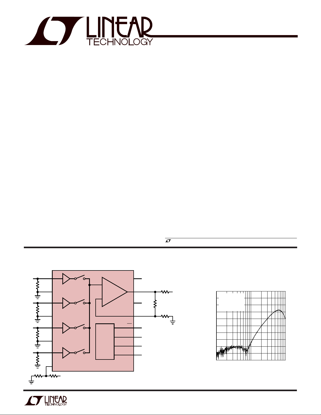
The LT®1204 is a 4-input video multiplexer designed to
drive 75Ω cables and easily expand into larger routing
systems. Wide bandwidth, high slew rate, and low differential gain and phase make the LT1204 ideal for broadcast
quality signal routing. Channel separation and disable
isolation are greater than 90dB up to 10MHz. The channelto-channel output switching transient is only 40mV
with a 50ns duration, making the transition imperceptible
on high quality monitors.
A unique feature of the LT1204 is its ability to expand into
larger routing matrices. This is accomplished by a patent
pending circuit that bootstraps the feedback resistors in
the disable condition, raising the true output impedance of
the circuit. The effect of this feature is to eliminate cable
misterminations in large systems.
The large input and output signal levels supported by the
LT1204 when operated on ±15V supplies make it ideal for
general purpose analog signal selection and multiplexing.
A shutdown feature reduces the supply current to 1.5mA.
P-P
,
, LTC and LT are registered trademarks of Linear Technology Corporation.
U
O
A
PPLICATITYPICAL
V
1
2
3
4
5
6
7
8
8.2k
IN0
GND
V
IN1
GND
V
IN2
GND
V
IN3
REF
+1
+1
+1
+1
–15V
+
CFA
–
LOGIC
LT1204
V
IN0
75Ω
V
IN1
75Ω
V
IN2
75Ω
V
IN3
75Ω
6.8k
S/D
ENABLE
16
+
15V
V
V
15
O
14
–
V
–15V
FB
13
12
11
A1
10
9
A0
1204 TA01
75Ω
V
OUT
R
F
1k
R
G
1k
–20
–40
–60
–80
–100
ALL HOSTILE CROSSTALK (dB)
–120
All Hostile Crosstalk
Surface Mount PCB Measurements
VS = ±15V
V
= GND
IN 0
= 0dBm
V
IN 1,2,3
= 100Ω
R
L
1
10 100
FREQUENCY (MHz)
1204 TA02
1
LT1204
A
W
O
LUTEXI TIS
S
A
WUW
U
ARB
G
Supply Voltage ..................................................... ±18V
– Input Current (Pin 13) .................................... ±15mA
+Input and Control/Logic Current (Note 1) ........ ±50mA
Output Short-Circuit Duration (Note 2).........Continuous
Specified Temperature Range (Note 3)....... 0°C to 70°C
WU
/
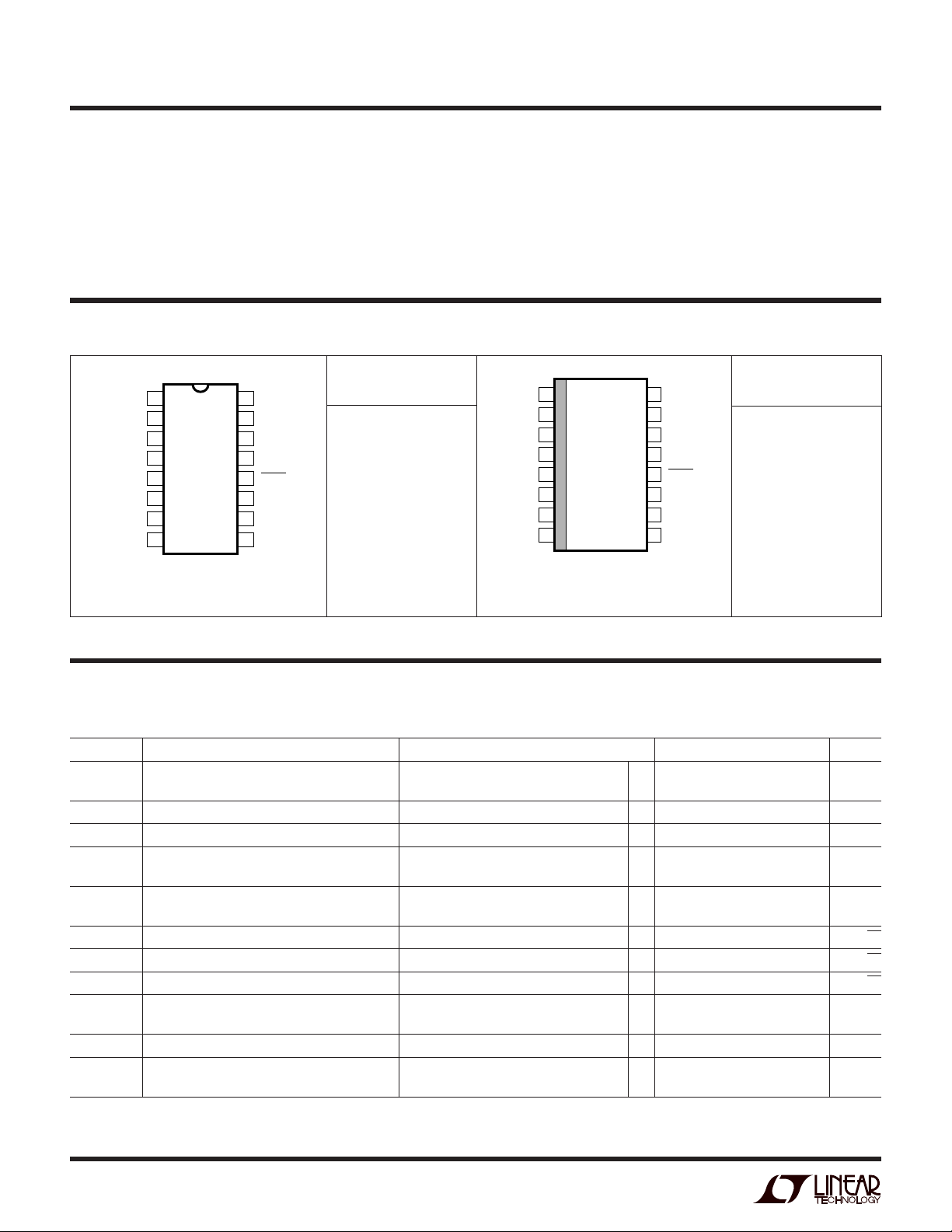
PACKAGE
V
IN0
GND
V
IN1
GND
V
IN2
GND
V
IN3
REF
T
JMAX
O
RDER I FOR ATIO
TOP VIEW
1
2
3
4
5
6
7
8
N PACKAGE
16-LEAD PDIP
= 150°C, θJA = 70°C/W
16
15
14
13
12
11
10
9
+
V
V
O
–
V
FB
SHDN
ENABLE
A1
A0
ORDER PART
NUMBER
LT1204CN*
*See Note 3 *See Note 3
Operating Temperature Range............... –40°C to 85°C
Storage Temperature Range................ –65°C to 150°C
Junction Temperature (Note 4)............................ 150°C
Lead Temperature (Soldering, 10 sec)..................300°C
U
V
1
IN0
GND
2
V
3
IN1
GND
4
V
5
IN2
GND
6
V
7
IN3
REF
8
16-LEAD PLASTIC SO
T
JMAX
TOP VIEW
16
15
14
13
12
11
10
9
SW PACKAGE
= 150°C, θJA = 90°C/W
+
V
V
O
–
V
FB
SHDN
ENABLE
A1
A0
ORDER PART
NUMBER
LT1204CSW*
Consult factory for Industrial and Military grade parts.
LECTRICAL C CHARA TERIST
E
ICS
0°C ≤ TA ≤ 70°C, ±5V ≤ VS ≤ ±15V, VCM = 0V, Pin 8 grounded and pulse tested unless otherwise noted.
SYMBOL PARAMETER CONDITIONS MIN TYP MAX UNITS
V
I
I
e
+i
–i
C
C
R
OS
IN
IN
n
IN
OUT
+
–
n
n
IN
Input Offset Voltage Any Positive Input, TA = 25°C514mV
● 16 mV
Offset Matching Between Any Positive Input, VS = ±15V ● 0.5 5 mV
Input Offset Voltage Drift Any Positive Input ● 40 µV/°C
Positive Input Bias Current Any Positive Input, TA = 25°C38µA
● 10 µA
Negative Input Bias Current TA = 25°C ±20 ±100 µA
● ±150 µA
Input Noise Voltage f = 1kHz, RF = 1k, RG = 10Ω, RS = 0Ω 7 nV/√Hz
Noninverting Input Noise Current Density f = 1kHz 1.5 pA/√Hz
Inverting Input Noise Current Density f = 1kHz 40 pA/√Hz
Input Capacitance Input Selected 3.0 pF
Input Deselected 3.5 pF
Output Capacitance Disabled, Pin 11 Voltage = 0V 8 pF
Positive Input Resistance, Any Positive Input VS = ±5V, VIN = –1.5V, 2V, TA = 25°C520 MΩ
= ±15V, VIN = ±5V ● 420 MΩ
V
S
2
LT1204
LECTRICAL C CHARA TERIST
E
0°C ≤ TA ≤ 70°C, ±5V ≤ VS ≤ ±15V, VCM = 0V, Pin 8 grounded and pulse tested unless otherwise noted.
SYMBOL PARAMETER CONDITIONS MIN TYP MAX UNITS
Input Voltage Range, Any Positive Input VS = ±5V, TA = 25°C 2.0 2.5 V
CMRR Common Mode Rejection Ratio VS = ±5V, VCM = –1.5V, 2V, TA = 25°C4855 dB
Negative Input Current VS = ±5V, VCM = –1.5V, 2V, TA = 25°C 0.05 1 µA/V
Common Mode Rejection V
PSRR Power Supply Rejection Ratio VS = ±4.5V to ±15V ● 60 76 dB
Negative Input Current Power Supply Rejection VS = ±4.5V to ±15V ● 0.5 5 µA/V
A
R
V
I
I
VOL
OL
OUT
OUT
S
Large-Signal Voltage Gain VS = ±15V, V
Transresistance VS = ±15V, V
∆V
Output Voltage Swing VS = ±15V, RL = 400Ω, TA = 25°C ±12 ±13.5 V
Output Current RL = 0Ω, TA = 25°C 35 55 125 mA
Supply Current (Note 5) Pin 11 = 5V ● 19 24 mA
Disabled Output Resistance VS = ±15V, Pin 11 = 0V, VO = ±5V,
–
/∆I
O
IN
ICS
–1.5 –2.0 V
VS = ±15V ● ±5.0 ±6.0 V
= ±15V, Pin 8 Voltage = –5V ● 3.75 4.0 V
V
S
V
= ±15V, VCM = ±5V ● 48 58 dB
S
= ±15V, VCM = ±5V ● 0.05 1 µA/V
S
= ±10V, RL = 1k ● 57 73 dB
= ±5V, V
V
S
VS = ±5V, V
VS = ±5V, RL = 150Ω, TA = 25°C ±3.0 ±3.7 V
Pin 11 = 0V
Pin 12 = 0V
R
= RG = 1k ● 14 25 kΩ
F
VS = ±15V, Pin 11 = 0V, VO = ±5V,
R
= 2k, RG = 222Ω ● 820 kΩ
F
OUT
= ±2V, RL = 150Ω ● 57 66 dB
OUT
= ±10V, RL = 1k ● 115 310 kΩ
OUT
= ±2V, RL = 150Ω ● 115 210 kΩ
OUT
● ±10 V
● ±2.5 V
● 19 24 mA
● 1.5 3.5 mA
U
DIGITAL I PUT CHARACTERISTICS
0°C ≤ TA ≤ 70°C, VS = ±15V, RF = 2k, RG = 220Ω, RL = 400Ω unless otherwise noted.
SYMBOL PARAMETER CONDITIONS MIN TYP MAX UNITS
V
IL
V
IH
I
IL
I
IH
I
SHDN
t
sel
t
dis
t
en
t
SHDN
Input Low Voltage Pins 9, 10, 11, 12 ● 0.8 V
Input High Voltage Pins 9, 10, 11, 12 ● 2V
Input Low Current Pins 9, 10 Voltage = 0V ● 1.5 6 µA
Input High Current Pins 9, 10 Voltage = 5V ● 10 150 nA
Enable Low Input Current Pin 11 Voltage = 0V ● 4.5 15 µA
Enable High Input Current Pin 11 Voltage = 5V ● 200 300 µA
Shutdown Input Current Pin 12 Voltage 0V ≤ V
Channel-to-Channel Select Time (Note 6) Pin 8 Voltage = –5V, TA = 25°C 120 240 ns
Disable Time (Note 7) Pin 8 Voltage = –5V, TA = 25°C 40 100 ns
Enable Time (Note 8) Pin 8 Voltage = –5V, TA = 25°C 110 200 ns
Shutdown Assert or Release Time (Note 9) Pin 8 Voltage = –5V, TA = 25°C 1.4 10 µs
≤ 5V ● 20 80 µA
SHDN
3

LT1204
AC CHARACTERISTICS
SYMBOL PARAMETER CONDITIONS MIN TYP MAX UNITS
tr, t
f
SR Slew Rate (Note 10) RL = 400Ω 400 1000 V/µs
t
S
The ● denotes specifications which apply over the specified operating
temperature range.
Note 1: Analog and digital inputs (Pins 1, 3, 5, 7, 9, 10, 11 and 12) are
protected against ESD and overvoltage with internal SCRs. For inputs
< ±6V the SCR will not fire, voltages above 6V will fire the SCRs and
the DC current should be limited to 50mA. To turn off the SCR the pin
voltage must be reduced to less than 2V or the current reduced to less
than 10mA.
Note 2: A heat sink may be required depending on the power supply
voltage.
Note 3: Commercial grade parts are designed to operate over the
temperature range of –40°C to 85°C but are neither tested nor
guaranteed beyond 0°C to 70°C. Industrial grade parts specified and
tested over –40°C to 85°C are available on special request. Consult
factory.
Note 4: T
dissipation P
LT1204CN: T
LT1204CS: T
Note 5: The supply current of the LT1204 has a negative temperature
coefficient. For more information see Typical Performance
Characteristics.
Note 6: Apply 0.5V DC to Pin 1 and measure the time for the
appearance of 5V at Pin 15 when Pin 9 goes from 5V to 0V. Pin 10
Voltage = 0V. Apply 0.5V DC to Pin 3 and measure the time for the
appearance of 5V at Pin 15 when Pin 9 goes from 0V to 5V. Pin 10
Voltage = 0V. Apply 0.5V DC to Pin 5 and measure the time for the
Small-Signal Rise and Fall Time RL = 150Ω, V
Channel Select Output Transient All VIN = 0V, RL = 400Ω, Input Referred 40 mV
Settling Time 0.1%, V
All Hostile Crosstalk (Note 11) SO PCB #028, RL = 100Ω, RS = 10Ω 92 dB
Disable Crosstalk (Note 11) SO PCB #028, Pin 11 Voltage = 0V, RL = 100Ω, RS = 50Ω 95 dB
Shutdown Crosstalk (Note 11) SO PCB #028, Pin 12 Voltage = 0V, RL = 100Ω, RS = 50Ω 92 dB
All Hostile Crosstalk (Note 11) PDIP PCB #029, RL = 100Ω, RS = 10Ω 76 dB
Disable Crosstalk (Note 11) PDIP PCB #029, Pin 11 Voltage = 0V, RL = 100Ω, RS = 50Ω 81 dB
Shutdown Crosstalk (Note 11) PDIP PCB #029, Pin 12 Voltage = 0V, RL = 100Ω, RS = 50Ω 76 dB
Differential Gain (Note 12) VS = ±15V, RL = 150Ω 0.04 %
Differential Phase (Note 12) VS = ±15V, RL = 150Ω 0.06 DEG
is calculated from the ambient temperature TA and power
J
according to the following formulas:
D
= TA + (PD)(70°C/W)
J
= TA + (PD)(90°C/W)
J
TA = 25°C, VS = ±15V, RF = RG = 1k, unless otherwise noted.
= ±125mV 5.6 ns
OUT
= 10V, RL = 1k 70 ns
OUT
= ±5V, RL = 150Ω 0.04 %
V
S
= ±5V, RL = 150Ω 0.12 DEG
V
S
appearance of 5V at Pin 15 when Pin 9 goes from 5V to 0V. Pin 10
Voltage = 5V. Apply 0.5V DC to Pin 7 and measure the time for the
appearance of 5V at Pin 15 when Pin 9 goes from 0V to 5V. Pin 10
Voltage = 5V.
Note 7: Apply 0.5V DC to Pin 1 and measure the time for the
disappearance of 5V at Pin 15 when Pin 11 goes from 5V to 0V.
Pins 9 and 10 are at 0V.
Note 8: Apply 0.5V DC to Pin 1 and measure the time for the
appearance of 5V at Pin 15 when Pin 11 goes from 0V to 5V.
Pins 9 and 10 are at 0V. Above a 1MHz toggle rate, t
Note 9: Apply 0.5V DC at Pin 1 and measure the time for the
appearance of 5V at Pin 15 when Pin 12 goes from 0V to 5V.
Pins 9 and 10 are at 0V. Then measure the time for the disappearance
of 5V DC to 500mV at Pin 15 when Pin 12 goes from 5V to 0V.
Note 10: Slew rate is measured at ±5V on a ±10V output signal while
operating on ±15V supplies with R
Note 11: VIN = 0dBm (0.223V
4th input selected. For Disable crosstalk and Shutdown crosstalk all 4
inputs are driven simultaneously. A 6dB output attenuator is formed by
a 50Ω series output resistor and the 50Ω input impedance of the
HP4195A Network Analyzer. R
Note 12: Differential Gain and Phase are measured using a Tektronix
TSG120 YC/NTSC signal generator and a Tektronix 1780R Video
Measurement Set. The resolution of this equipment is 0.1% and 0.1°.
Five identical MUXs were cascaded giving an effective resolution of
0.02% and 0.02°.
= 2k, RG = 220Ω and RL = 400Ω.
F
) at 10MHz on any 3 inputs with the
RMS
= RG = 1k.
F
reduces.
en
4
U
W
TYPICAL AC PERFOR A CE
V
(V) A
S
±15 1 150 1.1k None 88.5 48.3 0.1
±12 1 150 976 None 82.6 49.1 0.1
±5 1 150 665 None 65.5 43.6 0.1
±15 2 150 787 787 75.7 45.8 0
±12 2 150 750 750 71.9 45.0 0
±5V 2 150 590 590 58.0 32.4 0
±15 10 150 866 95.3 44.3 28.7 0.1
±12 10 150 825 90.9 43.5 27.2 0
±5 10 150 665 73.2 37.2 22.1 0
V
RL (Ω)R
1k 1.6k None 95.6 65.8 0
1k 1.3k None 90.2 63.6 0.1
1k 866 None 68.2 42.1 0.1
1k 887 887 82.2 61.3 0.1
1k 845 845 77.5 52.1 0
1k 649 649 62.1 42.7 0.1
1k 1k 110 47.4 30.9 0.1
1k 931 100 46.3 32.1 0.1
1k 750 82.5 39.3 27.8 0.1
(Ω)R
F
Measurements taken from SO Demonstration Board #028.
SMALL SIGNAL SMALL SIGNAL SMALL SIGNAL
(Ω) –3dB BW (MHz) 0.1dB BW (MHz) PEAKING (dB)
G
LT1204
TRUTH TABLE
CHANNEL
A1 A0 ENABLE SHUTDOWN SELECTED
00 1 1 V
01 1 1 V
10 1 1 V
11 1 1 V
X X 0 1 High Z Output
X X X 0 Off
IN0
IN1
IN2
IN3
5

LT1204
FREQUENCY (Hz)
1M
–2
GAIN (dB)
–1
0
1
2
10M 100M 1G
1204 G04
–3
–4
–5
–6
3
4
–120
PHASE (DEG)
–100
–80
–60
–40
–140
–160
–180
–200
–20
0
PHASE
GAIN
VS = ±5V
R
L
= 150Ω
R
F
= 655Ω
FREQUENCY (Hz)
1M
18
GAIN (dB)
19
20
21
22
10M 100M 1G
1204 G06
17
16
15
14
23
24
–120
PHASE (DEG)
–100
–80
–60
–40
–140
–160
–180
–200
–20
0
GAIN
VS = ±5V
R
L
= 150Ω
R
F
= 665Ω
R
G
= 73.2Ω
PHASE
LPER
UW
R
F
O
ATYPICA
CCHARA TERIST
E
C
ICS
±12V Frequency Response, AV = 1
4
3
2
1
0
–1
GAIN (dB)
–2
–3
–4
–5
–6
1M
PHASE
GAIN
10M 100M 1G
FREQUENCY (Hz)
VS = ±12V
= 150Ω
R
L
= 976Ω
R
F
1204 G01
0
–20
–40
–60
–80
–100
–120
–140
–160
–180
–200
PHASE (DEG)
±5V Frequency Response, AV = 1
±12V Frequency Response, AV = 2 ±5V Frequency Response, AV = 2
10
9
8
7
6
5
GAIN (dB)
4
3
2
1
0
1M
VS = ±12V
= 150Ω
R
GAIN
L
= 750Ω
R
F
= 750Ω
R
G
1204 G02
PHASE
10M 100M 1G
FREQUENCY (Hz)
0
–20
–40
–60
–80
–100
–120
–140
–160
–180
–200
PHASE (DEG)
10
9
8
7
6
5
GAIN (dB)
4
3
2
1
0
1M
PHASE
GAIN
10M 100M 1G
FREQUENCY (Hz)
VS = ±5V
= 150Ω
R
L
= 590Ω
R
F
= 590Ω
R
G
1204 G05
0
–20
–40
–60
–80
–100
–120
–140
–160
–180
–200
PHASE (DEG)
±12V Frequency Response, AV = 10
24
23
22
21
20
19
GAIN (dB)
18
17
16
15
14
1M
6
PHASE
GAIN
10M 100M 1G
FREQUENCY (Hz)
VS = ±12V
= 150Ω
R
L
= 825Ω
R
F
= 90.9Ω
R
G
1204 G03
0
–20
–40
–60
–80
–100
–120
–140
–160
–180
–200
±5V Frequency Response, AV = 10
PHASE (DEG)
 Loading...