

Linear Technology LT1187 Datasheet
LT1187
FREQUENCY (MHz)
0
VOLTAGE GAIN (dB)
10
20
30
40
0.1 10 100
LT1187 • TA02
–10
1
VS = ±5V
R
L
= 1k
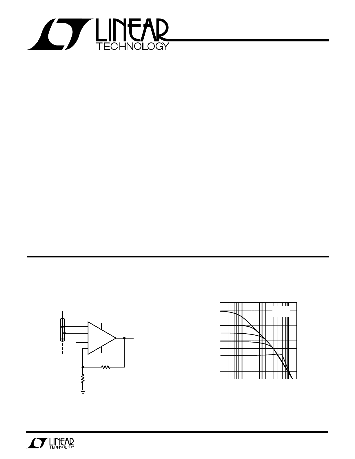
Low Power
Video Difference Amplifier
EATU
F
■
Differential or Single-Ended Gain Block (Adjustable)
■
–3dB Bandwidth, AV = ±2 50MHz
■
Slew Rate 165V/µs
■
Low Supply Current 13mA
■
Output Current ±20mA
■
CMRR at 10MHz 40dB
■
LT1193 Pin Compatible
■
Low Cost
■
Single 5V Operation
■
Drives Cables Directly
■
Output Shutdown
PPLICATI
A
■
Line Receivers
■
Video Signal Processing
■
Cable Drivers
■
Tape and Disc Drive Systems
RE
S
O
U
S
DUESCRIPTIO
The LT1187 is a difference amplifier optimized for operation on ± 5V, or a single 5V supply, and gain ≥ 2. This
versatile amplifier features uncommitted high input impedance (+) and (–) inputs, and can be used in differential
or single-ended configurations. Additionally, a second set
of inputs give gain adjustment and DC control to the
difference amplifier.
The LT1187’s high slew rate, 165V/µs, wide bandwidth,
50MHz, and ±20mA output current require only 13mA of
supply current. The shutdown feature reduces the power
dissipation to a mere 15mW, and allows multiple amplifiers to drive the same cable.
The LT1187 is a low power version of the popular LT1193,
and is available in 8-pin miniDIPs and SO packages. For
applications with gains of 10 or more, see the LT1189
data sheet.
CABLE
V
A
IN
PPLICATITYPICAL
with DC Adjust
V
DC
U
O
Closed-Loop Gain vs FrequencyCable Sense Amplifier for Loop Through Connections
5V
3
+
1k
–
LT1187
+
–
–5V
7
6
4
1k
V
LT1187 • TA01
OUT
2
1
8
1
LT1187
WU
U
PACKAGE
/
O
RDER I FOR ATIO
W
O
A
LUTEXI T
S
Total Supply Voltage (V+ to V–) ............................. 18V
Differential Input Voltage ........................................ ±6V
Input Voltage .......................................................... ±V
Output Short Circuit Duration (Note 1) ........ Continuous
Operating Temperature Range
LT1187M..................................... –55°C to 150°C
LT1187C............................................. 0°C to 70°C
Junction Temperature (Note 2)
Plastic Package (CN8,CS8) ......................... 150°C
Ceramic Package (CJ8,MJ8) ....................... 175°C
Storage Temperature Range ................ – 65°C to 150°C
Lead Temperature (Soldering, 10 sec.)................ 300°C
+
5V
–
VS = ±5V, V
SYMBOL PARAMETER CONDITIONS MIN TYP MAX UNITS
V
OS
I
OS
I
B
e
n
i
n
R
IN
C
IN
VIN
LIM
CMRR Common-Mode Rejection Ratio VCM = –2.5V to 3.5V 70 100 dB
PSRR Power Supply Rejection Ratio VS = ±2.375V to ±8V 70 85 dB
V
OUT
G
E
SR Slew Rate (Note 6, 10) 100 165 V/µs
FPBW Full Power Bandwidth VO = 1V
BW Small Signal Bandwidth AV = 10 5.7 MHz
tr, t
f
t
PD
t
s
Diff A
Diff Ph Differential Phase RL = 1k, AV = 4, (Note 9) 0.8 DEG
I
S
LECTRICAL C CHARA TERIST
E
= 0V, R
REF
Input Offset Voltage Either Input, (Note 4) 2.0 10 mV
Input Offset Current Either Input 0.2 1.0 µA
Input Bias Current Either Input ±0.5 ±2.0 µA
Input Noise Voltage fO = 10kHz 65 nV/√Hz
Input Noise Current fO = 10kHz 1.5 pA/√Hz
Input Resistance Differential 100 kΩ
Input Capacitance Either Input 2.0 pF
Input Voltage Limit (Note 5) ±380 mV
Input Voltage Range –2.5 3.5 V
Output Voltage Swing VS = ±5V, RL = 1k, AV = 50 ±3.8 ±4.0 V
Gain Error VO = ±1V, AV = 10, RL = 1k 0.2 1.0 %
Rise Time, Fall Time AV = 50, VO = ±1.5V, 20% to 80% (Note 10) 150 230 325 ns
Propagation Delay RL= 1k, VO = ±125mV, 50% to 50% 26 ns
Overshoot VO = ±50mV 0 %
Settling Time 3V Step, 0.1%, (Note 8) 100 ns
V
Differential Gain RL = 1k, AV = 4, (Note 9) 0.6 %
Supply Current 13 16 mA
Shutdown Supply Current Pin 5 at V
A
= 900Ω from pins 6 to 8, R
FB1
WUW
U
ARB
G
S
I
TOP VIEW
1+/REF
S
8-LEAD HERMETIC DIP
Consult factory for Industrial grade parts.
ICS
TA = 25°C, (Note 3)
= 100Ω from pin 8 to ground, RL = R
FB2
SOIC Package 2.0 11 mV
VS = ±8V, RL = 1k, AV = 50 ±6.7 ±7.0
VS = ±8V, RL = 300Ω, AV = 50, (Note 3) ±6.4 ±6.8
, (Note 7) 53 MHz
P-P
–
2
–IN
+IN
3
–
V
J8 PACKAGE
8-LEAD PLASTIC SOIC
T
= 175°C, θJA = 100°C/W (J8)
JMAX
= 150°C, θJA = 100°C/W (N8)
T
JMAX
T
= 150°C, θJA = 150°C/W (S8)
JMAX
8-LEAD PLASTIC DIP
S8 PACKAGE
–/FB
8
7
V
6
OUT
54
S/D
N8 PACKAGE
LT1187 • POI01
+ R
FB1
+
= 1k, CL ≤ 10pF, pin 5 open.
FB2
ORDER PART
NUMBER
LT1187MJ8
LT1187CJ8
LT1187CN8
LT1187CS8
S8 PART MARKING
1187
LT1187M/C
0.8 1.5 mA
P-P
2
LT1187
+
5V
–
VS = ±5V, V
SYMBOL PARAMETER CONDITIONS MIN TYP MAX UNITS
I
S/D
t
ON
t
OFF
LECTRICAL C CHARA TERIST
E
= 0V, R
REF
Shutdown Pin Current Pin 5 at V
Turn On Time Pin 5 from V– to Ground, RL = 1k 500 ns
Turn Off Time Pin 5 from Ground to V–, RL = 1k 600 ns
= 900Ω from pins 6 to 8, R
FB1
ICS
TA = 25°C, (Note 3)
= 100Ω from pin 8 to ground, RL = R
FB2
–
FB1
+ R
= 1k, CL ≤ 10pF, pin 5 open.
FB2
LT1187M/C
525 µA
5V
V
LECTRICAL C CHARA TERIST
E
+
= 5V, V
S
–
= 0V, V
S
= 2.5V, R
REF
= 900Ω from pins 6 to 8, R
FB1
ICS
open.
SYMBOL PARAMETER CONDITIONS MIN TYP MAX UNITS
V
OS
I
OS
I
B
CMRR Common-Mode Rejection Ratio VCM = 2.0V to 3.5V 70 100 dB
V
OUT
SR Slew Rate VO = 1.5V to 3.5V 130 V/µs
BW Small-Signal Bandwidth AV = 10 5.3 MHz
I
S
I
S/D
+
5V
–
VS = ±5V, V
SYMBOL PARAMETER CONDITIONS MIN TYP MAX UNITS
V
OS
∆VOS/∆T Input V
I
OS
I
B
CMRR Common-Mode Rejection Ratio VCM = –2.5V to 3.5V 70 100 dB
PSRR Power Supply Rejection Ratio VS = ±2.375V to ±8V 60 85 dB
V
OUT
G
E
I
S
I
S/D
Input Offset Voltage Either Input, (Note 4) 2.0 10 mV
SOIC Package 2.0 12 mV
Input Offset Current Either Input 0.2 1.0 µA
Input Bias Current Either Input ±0.5 ±2.0 µA
Input Voltage Range 2.0 3.5 V
Output Voltage Swing RL = 300Ω to Ground V
(Note 3)
Supply Current 12 15 mA
Shutdown Supply Current Pin 5 at V
Shutdown Pin Current Pin 5 at V
LECTRICAL C CHARA TERIST
E
= 0V, R
REF
Input Offset Voltage Either Input, (Note 4) 2.0 15 mV
Input Offset Current Either Input 0.2 1.5 µA
Input Bias Current Either Input ±0.5 ±3.5 µA
Input Voltage Range –2.5 3.5 V
Output Voltage Swing VS = ±5V, RL = 1k, AV = 50 ±3.7 ±4.0 V
Gain Error VO = ±1V, AV = 10, RL = 1k 0.2 1.2 %
Supply Current 13 17 mA
Shutdown Supply Current Pin 5 at V–, (Note 11) 0.8 1.5 mA
Shutdown Pin Current Pin 5 at V
= 900Ω from pins 6 to 8, R
FB1
Drift 8.0 µV/°C
OS
VS = ±8V, RL = 1k, AV = 50 ±6.6 ±7.0
VS = ±8V, RL = 300Ω, AV = 50, (Note 3) ±6.4 ±6.8
–
–
= 100Ω from pin 8 to ground, RL = R
FB2
–
TA = 25°C, (Note 3)
= 100Ω from pin 8 to V
FB2
ICS
–55°C ≤ TA ≤ 125°C, (Note 3)
, RL = R
REF
High 3.6 4.0 V
OUT
Low 0.15 0.4
V
OUT
FB1
+ R
= 1k, CL ≤ 10pF, pin 5
FB2
LT1187M/C
0.8 1.5 mA
525 µA
= 1k, CL ≤ 10pF, pin 5 open.
LT1187M
525 µA
+ R
FB1
FB2
3
LT1187
+
5V
–
V
= ±5V, V
S
SYMBOL PARAMETER CONDITIONS MIN TYP MAX UNITS
V
OS
∆VOS/∆T Input V
I
OS
I
B
CMRR Common-Mode Rejection Ratio VCM = –2.5V to 3.5V 70 100 dB
PSRR Power Supply Rejection Ratio VS = ±2.375V to ±8V 65 85 dB
V
OUT
G
E
I
S
I
S/D
LECTRICAL C CHARA TERIST
E
= 0V, R
REF
Input Offset Voltage Either Input, (Note 4) 2.0 12 mV
Input Offset Current Either Input 0.2 1.5 µA
Input Bias Current Either Input ±0.5 ±3.5 µA
Input Voltage Range –2.5 3.5 V
Output Voltage Swing VS = ±5V, RL = 1k, AV = 50 ±3.7 ±4.0 V
Gain Error VO = ±1V, AV = 10, RL = 1k 0.2 1.0 %
Supply Current 13 17 mA
Shutdown Supply Current Pin 5 at V–, (Note 11) 0.8 1.5 mA
Shutdown Pin Current Pin 5 at V
= 900Ω from pins 6 to 8, R
FB1
Drift 9.0 µV/°C
OS
VS = ±8V, RL = 1k, AV = 50 ±6.6 ±7.0
VS = ±8V, RL = 300Ω, AV = 50, (Note 3) ±6.4 ±6.8
ICS
= 100Ω from pin 8 to ground, RL = R
FB2
–
0°C ≤ TA ≤ 70°C, (Note 3)
FB1
+ R
= 1k, CL ≤ 10pF, pin 5 open.
FB2
LT1187C
525 µA
LECTRICAL C CHARA TERIST
E
5V
+
V
= 5V, V
S
SYMBOL PARAMETER CONDITIONS MIN TYP MAX UNITS
V
OS
∆VOS/∆T Input V
I
OS
I
B
CMRR Common-Mode Rejection Ratio VCM = 2.0V to 3.5V 70 100 dB
V
OUT
I
S
I
S/D
Note 1: A heat sink may be required to keep the junction temperature below
absolute maximum when the output is shorted continuously.
Note 2: T
according to the following formulas:
P
D
Note 3: When R
= 300Ω is specified, then an additional 430Ω is added to the output such
R
L
that (R
Note 4: V
pair, and is input referred.
Note 5: V
pin 3) for which the output can respond.
–
= 0V, V
S
Input Offset Voltage Either Input, (Note 4) 2.0 12.0 mV
Input Offset Current Either Input 0.2 1.5 µA
Input Bias Current Either Input ±0.5 ±3.5 µA
Input Voltage Range 2.0 3.5 V
Output Voltage Swing RL = 300Ω to Ground V
Supply Current 12 16 mA
Shutdown Supply Current Pin 5 at V–, (Note 11) 0.8 1.5 mA
Shutdown Pin Current Pin 5 at V
is calculated from the ambient temperature TA and power dissipation
J
LT1187MJ8,LT1187CJ8: T
LT1187CN8: T
LT1187CS8: T
= 1k is specified, the load resistor is R
L
+ R
FB1
) in parallel with 430Ω is RL = 300Ω.
FB2
measured at the output (pin 6) is the contribution from both input
OS
is the maximum voltage between –VIN and +VIN (pin 2 and
IN LIM
= 2.5V, R
REF
Drift 9.0 µV/°C
OS
= 900Ω from pins 6 to 8, R
FB1
= TA + (PD × 100°C/W)
J
= TA + (PD × 100°C/W)
J
= TA + (PD × 150°C/W)
J
FB1
+ R
ICS
0°C ≤ TA ≤ 70°C, (Note 3)
= 100Ω from pin 8 to V
FB2
SOIC Package 2.0 13.0 mV
OUT
(Note 3) V
–
Note 6: Slew rate is measured between ±0.5V on the output, with a V
of ±0.75V, A
Note 7: Full power bandwidth is calculated from the slew rate measurement:
FPBW = SR/2πVp.
Note 8: Settling time measurement techniques are shown in “Take the
Guesswork Out of Settling Time Measurements,” EDN, September 19, 1985.
, but when
FB2
Note 9: NTSC (3.58MHz).
Note 10: AC parameters are 100% tested on the ceramic and plastic DIP
packaged parts (J8 and N8 suffix) and are sample tested on every lot of the SO
packaged parts (S8 suffix).
Note 11: See Application section for shutdown at elevated temperatures. Do
not operate shutdown above T
OUT
= 3 and RL = 1k.
V
, RL = R
REF
High 3.5 4.0 V
Low 0.15 0.4
+ R
FB1
> 125°C.
J
= 1k, CL ≤ 10pF, pin 5 open.
FB2
LT1187C
525 µA
IN
step
4
 Loading...