

Linear Technology LT1185 Datasheet
LT1185
Low Dropout Regulator
EATU
F
■
Low Resistance Pass Transistor: 0.25Ω
■
Dropout Voltage: 0.75V at 3A
■
±1% Reference Voltage
■
Accurate Programmable Current Limit
■
Shutdown Capability
■
Internal Reference Available
■
Standard 5-Lead Packages
■
Full Remote Sense
■
Low Quiescent Current: ≈2.5mA
■
Good High Frequency Ripple Rejection
RE
S
DUESCRIPTIO
The LT®1185 is a 3A low dropout regulator with adjustable
current limit and remote sense capability. It can be used as
a positive output regulator with floating input or as a
standard negative regulator with grounded input. The
output voltage range is 2.5V to 25V, with ±1% accuracy on
the internal reference voltage.
The LT1185 uses a saturation-limited NPN transistor as
the pass element. This device gives the linear dropout
characteristics of an FET pass element with significantly
less die area. High efficiency is maintained by using special
anti-saturation circuitry that adjusts base drive to track
load current. The “on resistance” is typically 0.25Ω.
Accurate current limit is programmed with a single 1/8W
external resistor, with a range of zero to three amperes. A
second, fixed internal limit circuit prevents destructive
currents if the programming current is accidentally overranged. Shutdown of the regulator output is guaranteed
when the program current is less than 1µA, allowing
external logic control of output voltage.
The LT1185 has all the protection features of previous LTC
regulators, including power limiting and thermal shutdown. The 4-lead TO-3 package is specified for –55°C to
150°C operation and the 5-lead TO-220 is specified over
0°C to 125°C.
, LTC and LT are registered trademarks of Linear Technology Corporation.
+
+
V
IN
6V TO 16V
–
*CURRENT LIMIT = 15k/R
U
O
A
PPLICATITYPICAL
5V, 3A Regulator with 3.5A Current Limit
C2
2µF
TANT
R
*
LIM
4.3k
REF GND
V
LT1185
IN
= 3.5A
LIM
R1
2.37k
+
FB
R2
2.67k
V
OUT
C1
2µF
TANT
5V AT 3A
LT1185 • TA01
Dropout Voltage
+
V
OUT
–
(V)
OUT
–V
IN
V
1.6
1.4
1.2
1.0
0.8
0.6
0.4
0.2
TJ = 25°C
TJ = 125°C
TJ = –55°C
0
0
1
2
LOAD CURRENT (A)
3
LT1185 • TA02
4
1
LT1185
A
W
O
LUTEXI TIS
S
A
WUW
U
ARB
G
(Note 1)
Input Voltage .......................................................... 35V
Input-Output Differential ......................................... 30V
FB Voltage ................................................................ 7V
REF Voltage .............................................................. 7V
Output Voltage........................................................ 30V
Output Reverse Voltage ............................................ 2V
Operating Ambient Temperature Range
LT1185C ............................................... 0°C to 70°C
LT1185M ......................................... –55°C to 125°C
Operating Junction Temperature Range*
Control Section
LT1185C ............................................. 0°C to 125°C
LT1185I .......................................... –40°C to 125°C
LT1185M ........................................ –55°C to 150°C
Power Transistor Section
LT1185C ............................................. 0°C to 150°C
LT1185I .......................................... –40°C to 150°C
LT1185M ........................................ –55°C to 175°C
Storage Temperature Range ................ – 65°C to 150°C
Lead Temperature (Soldering, 10 sec)................ 300°C
*See Application Section for details on calculating Operation Junction Temperature
/
PACKAGE
GND FB
V
OUT
4-LEAD TO-3 METAL CAN
θ
TAB IS V
IN
θ
O
RDER I FOR ATIO
BOTTOM VIEW
1
4
K PACKAGE
JC MAX
5-LEAD PLASTIC TO-220
JC MAX
2
3
= 2.5°C/W, θJA = 35°C/W
FRONT VIEW
5
4
3
2
1
T PACKAGE
= 2.5°C/W, θJA = 50°C/W
REF
V
IN
(CASE)
REF
V
OUT
V
IN
FB
GND
WU
U
ORDER PART
NUMBER
LT1185MK
ORDER PART
NUMBER
LT1185CT
LT1185IT
ELECTRICAL CHARACTERISTICS
The ● denotes specifications which apply over the operating temperature range, otherwise specifications are at TA = 25°C.
Adjustable version, VIN = 7.4V, V
PARAMETER CONDITIONS MIN TYP MAX UNITS
Reference Voltage (At FB Pin) 2.37 V
Reference Voltage Tolerance (At FB Pin) (Note 2) VIN – V
Feedback Pin Bias Current V
Droput Voltage (Note 3) I
Load Regulation (Note 7) I
Line Regulation (Note 7) VIN – V
Minimum Input Voltage I
Internal Current Limit (See Graph for 1.5V ≤ VIN – V
Guaranteed Curve) (Note 12)
OUT
= 5V, I
= 1mA, R
OUT
OUT
1mA ≤ I
OUT
V
– V
IN
OUT
P ≤ 25W (Note 6), V
≤ TJ ≤ T
T
MIN
= V
OUT
= 0.5A, V
OUT
= 3A, V
I
OUT
= 5mA to 3A 0.05 0.3 %
OUT
V
– V
IN
OUT
OUT
= 1A (Note 4), V
OUT
I
= 3A 4.3 V
OUT
– V
V
IN
OUT
V
– V
IN
OUT
– V
V
IN
OUT
= 4.02k, unless otherwise noted.
LIM
= 5V, V
≤ 3A ● 1 ±2.5 %
= 1.2V to VIN = 30V
REF
OUT
= 1.5V to 10V, V
= 1V to 20V, V
= 15V ● 2.0 3.0 4.2 A
= 20V ● 1.0 1.7 2.6 A
= 30V ● 0.2 0.4 1.0 A
= V
OUT
REF
= 5V
OUT
(Note 9)
MAX
● 0.7 2 µA
= 5V 0.20 0.37 V
OUT
= 5V 0.67 1.00 V
= 5V
OUT
= 5V 0.002 0.01 %/V
OUT
= V
OUT
REF
≤ 10V 3.3 3.6 4.2 A
OUT
● 3.1 4.4 A
0.3 ±1%
4.0 V
2
LT1185
ELECTRICAL CHARACTERISTICS
The ● denotes specifications which apply over the operating temperature range, otherwise specifications are at TA = 25°C.
Adjustable version, VIN = 7.4V, V
PARAMETER CONDITIONS MIN TYP MAX UNITS
External Current Limit 5k ≤ R
Programming Constant (Note 11)
External Current Limit Error 1A ≤ I
Quiescent Supply Current I
Supply Current Change with Load VIN – V
REF Pin Shutoff Current ● 0.4 2 7 µA
Thermal Regulation (See Applications VIN – V
Information) I
Reference Voltage Temperature Coefficient (Note 8) 0.003 0.01 %/°C
Thermal Resistance Junction to Case TO-3 Control Area 1 °C/W
OUT
= 5V, I
= 1mA, R
OUT
R
LIM
OUT
4V ≤ V
V
– V
IN
OUT
LIM
LIM
= 15k • A/I
= 5mA, V
IN
OUT
OUT
OUT
= 5mA to 2A
= 4.02k, unless otherwise noted.
LIM
≤ 15k, V
≤ 3A 0.02 I
= 1V ● 15k A•Ω
OUT
0.06 I
OUT
LIM
= V
REF
● 0.04 I
● 2.5 3.5 mA
LIM
LIM
0.09 I
LIM
LIM
+ 0.03 A
+ 0.05 A
≤ 25V (Note 5)
= V
(Note 10) ● 25 40 mA/A
SAT
≥ 2V ● 10 25 mA/A
= 10V 0.005 0.014 %/W
Power Transistor 3 °C/W
TO-220 Control Area 1 °C/W
Power Transistor 3 °C/W
Note 1: Absolute Maximum Ratings are those values beyond which the life
of a device may be impaired.
Note 2: Reference voltage is guaranteed both at nominal conditions (no
load, 25°C) and at worst-case conditions of load, line, power and
temperature. An intermediate value can be calculated by adding the effects
of these variables in the actual application. See the Applications
Information section of this data sheet.
Note 3: Dropout voltage is tested by reducing input voltage until the
output drops 1% below its nominal value. Tests are done at 0.5A and 3A.
The power transistor looks basically like a pure resistance in this range so
that minimum differential at any intermediate current can be calculated by
interpolation; V
= 0.25V + 0.25Ω • I
DROPOUT
. For load current less than
OUT
0.5A, see graph.
Note 4: “Minimum input voltage” is limited by base emitter voltage drive
of the power transistor section, not saturation as measured in Note 3. For
output voltages below 4V, “minimum input voltage” specification may limit
dropout voltage before transistor saturation limitation.
Note 5: Supply current is measured on the ground pin, and does not
include load current, R
, or output divider current.
LIM
Note 6: The 25W power level is guaranteed for an input-output voltage of
8.3V to 17V. At lower voltages the 3A limit applies, and at higher voltages
the internal power limiting may restrict regulator power below 25W. See
graphs.
Note 7: Line and load regulation are measured on a pulse basis with a
pulse width of ≈2ms, to minimize heating. DC regulation will be affected
by thermal regulation and temperature coefficient of the reference. See
Applications Information section for details.
Note 8: Guaranteed by design and correlation to other tests, but not
tested.
Note 9: T
= 0°C for the LT1185C, –40°C for LT1185I, and –55°C for
JMIN
the LT1185M. Power transistor area and control circuit area have different
maximum junction temperatures. Control area limits are T
= 125°C for
JMAX
the LT1185C and LT1185I and 150°C for the LT1185M. Power area limits
are 150°C for LT1185C and LT1185I and 175°C for LT1185M.
Note 10: V
0.25V + 0.25 • I
is the maximum specified dropout voltage;
SAT
.
OUT
Note 11: Current limit is programmed with a resistor from REF pin to GND
pin. The value is 15k/I
Note 12: For V
IN
.
LIM
– V
= 1.5V; VIN = 5V, V
OUT
= 3.5V. V
OUT
= 1V for all
OUT
other current limit tests.
3
LT1185
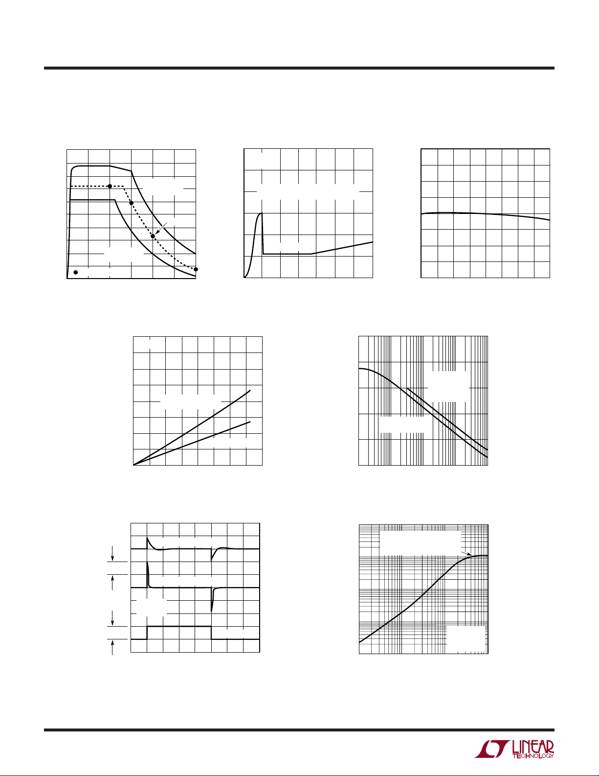
LPER
Internal Current Limit
5
4
3
2
OUTPUT CURRNT (A)
1
TEST POINTS
0
0
5
INPUT-OUTPUT DIFFERENTIAL (V)
F
GUARANTEED
LIMIT
15 20
10
R
O
GUARANTEED
LIMIT
TYPICAL
ATYPICA
25
LT1185 • TPC01
UW
CCHARA TERIST
E
C
Quiescent Ground Pin Current*
12
I
LOAD
= 25°C
T
J
10
*DOES NOT INCLUDE REF CURRENT
8
OR OUTPUT DIVIDER CURRENT
6
4
GROUND PIN CURRENT (mA)
2
0
0
30
510
= 0
V
= 5V
OUT
15 25
INPUT VOLTAGE (V)
ICS
20 30 35
LT1185 • TPC02
Feedback Pin Voltage
Temperature Drift
2.41
2.40
2.39
2.38
2.37
VOLTAGE (V)
2.36
2.35
2.34
2.33
–50
–25
0
JUNCTION TEMPERATURE (°C)
75
50
25
100
125
LT1185 • TPC03
150
Ground Pin Current
160
TJ = 25°C
140
120
100
0
REGULATOR JUST AT
DROPOUT POINT
1
LOAD CURRENT (A)
80
60
CURRENT (mA)
40
20
0
Load Transient Response
C
= 2.2µF, ESR = 1Ω
OUT
100mV
C
= 2.2µF, ESR = 2Ω
OUT
V
= 5V
OUT
= 1A
I
OUT
∆I
LOAD
0
26
4
2
8
TIME (µs)
VIN – V
10
= 5V
OUT
3
LT1185 • TPC04
0.1A tr,f ≤ 100ns
14
12
LT1185 • TPC06
Ripple Rejection vs Frequency
–100
–80
V
OUT
OUT
= 1.5V
ALL OUTPUT
VOLTAGES
WITH 0.05µF
ACROSS R2
= 5V
LT1185 • TPC05
(dB)
–60
IN
/V
OUT
–40
RATIO V
–20
0
4
100 10k 100k 1M
– V
V
IN
1k
FREQUENCY (Hz)
Output Impedance
10
1
0.1
IMPEDANCE (Ω)
0.01
16
0.001
1k
OUTPUT IMPEDANCE IS
SET BY OUTPUT CAPACITOR
ESR IN THIS REGION
V
OUT
I
OUT
C
OUT
FREQUENCY (Hz)
= 5V
= 1A
= 2.2µF
LT1183 • TPC07
1M10k 100k
4
UU W U
APPLICATIO S I FOR ATIO
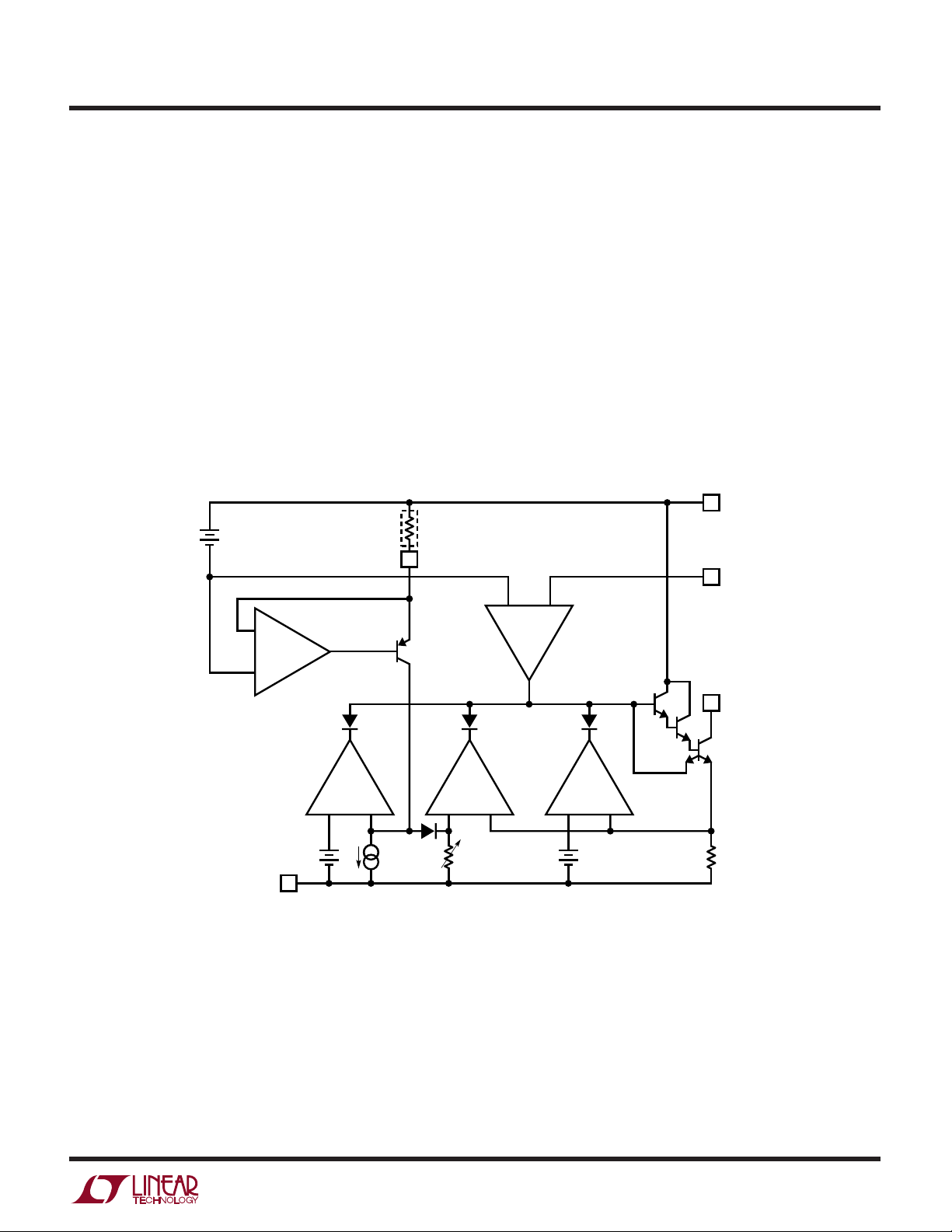
Block Diagram
LT1185
A simplified block diagram of the LT1185 is shown in
Figure 1. A 2.37V bandgap reference is used to bias the
input of the error amplifier A1, and the reference amplifier
A2. A1 feeds a triple NPN pass transistor stage which has
the two driver collectors tied to ground so that the main
pass transistor can completely saturate. This topology
normally has a problem with unlimited current in Q1 and
Q2 when the input voltage is less than the minimum
required to create a regulated output. The standard “fix”
for this problem is to insert a resistor in series with Q1 and
Q2 collectors, but this resistor must be low enough in
value to supply full base current for Q3 under worst-case
(EXTERNAL)
V
REF
2.37V
–
A2
+
R
LIM
REF
Q4
conditions, resulting in very high supply current when the
input voltage is low. To avoid this situation, the LT1185
uses an auxiliary emitter on Q3 to create a drive limiting
feedback loop which automatically adjusts the drive to Q1
so that the base drive to Q3 is just enough to saturate Q3,
but no more. Under saturation conditions, the auxiliary
emitter is acting like a collector to shunt away the output
current of A1. When the input voltage is high enough to
keep Q3 out of saturation, the auxiliary emitter current
drops to zero even when Q3 is conducting full load current.
GND
FB
+
–
A1
Q2
LT1185 • BD
Q3
R2
0.055Ω
V
OUT
Q1
D2 D4 D3
A5
+
–
300mV
V
IN
I1
2µA
A4
+
–
D1
R1
350Ω
+
A3
–
200mV
Figure 1. Block Diagram
5
 Loading...