

Linear Technology LT1175 Datasheet

LT1 1 75
500mA Negative
Low Dropout Micropower
FEATURES
■
Stable with Wide Range of Output Capacitors
■
Operating Current: 45µA
■
Shutdown Current: 10µA
■
Adjustable Current Limit
■
Positive or Negative Shutdown Logic
■
Low Voltage Linear Dropout Characteristics
■
Fixed 5V and Adjustable Versions
■
Tolerates Reverse Output Voltage
U
APPLICATIO S
■
Analog Systems
■
Modems
■
Instrumentation
■
A/D and D/A Converters
■
Interface Drivers
■
Battery-Powered Systems
, LTC and LT are registered trademarks of Linear Technology Corporation.
U
Regulator
DESCRIPTIO
The LT®1175 is a negative micropower low dropout regulator. It features 45µA quiescent current, dropping to
10µA in shutdown. A new reference amplifier topology
gives precision DC characteristics along with the ability to
maintain good loop stability with an extremely wide range
of output capacitors. Very low dropout voltage and high
efficiency are obtained with a unique power transistor antisaturation design. Adjustable and fixed 5V versions are
available.
Several new features make the LT1175 very user-friendly.
The SHDN pin can interface directly to either positive or
negative logic levels. Current limit is user-selectable at
200mA, 400mA, 600mA and 800mA. The output can be
forced to reverse voltage without damage or latchup.
Unlike some earlier designs, the increase in quiescent
current during a dropout condition is actively limited.
The LT1175 has complete blowout protection with current
limiting, power limiting and thermal shutdown. Special
attention was given to the problem of high temperature
operation with micropower operating currents,
output voltage rise under no-load conditions. The LT1175
is available in 8-pin PDIP and SO packages, 3-lead SOT223 as well as 5-pin surface mount DD and through-hole
TO-220 packages. The 8-pin SO package is specially
constructed for low thermal resistance.
preventing
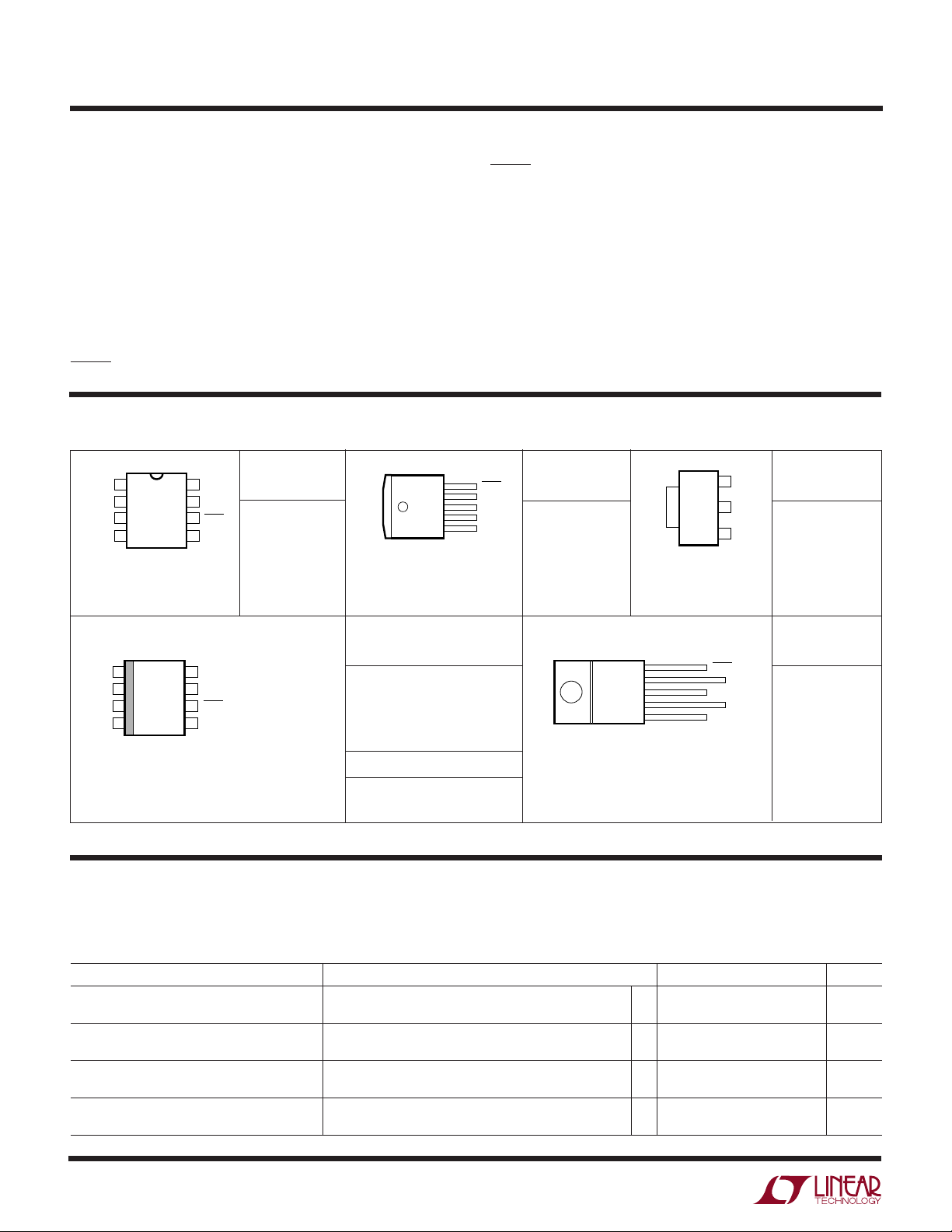
TYPICAL APPLICATIO
Typical LT1175 Connection
+ +
CIN*
SHDN GND
–V
IN
*C
IS NEEDED ONLY IF REGULATOR IS MORE THAN 6" FROM
IN
INPUT SUPPLY CAPACITOR. SEE APPLICATIONS INFORMATION
SECTION FOR DETAILS
INPUT
I
LIM2
I
LIM4
LT1175-5
SENSE
OUT
U
C
OUT
≥ 0.1µF
–5V
UP TO 500mA
1175 TA01
Minimum Input-to-Output Voltage
1.0
TJ = 25°C
, I
I
LIM2
0.8
0.6
0.4
0.2
INPUT-TO-OUTPUT VOLTAGE (V)
0
0
TIED TO V
LIM4
0.2
0.1
OUTPUT CURRENT (A)
0.3
IN
0.4
0.5
0.6
0.7
1175 TA02
1
LT1 1 75
1
2
3
FRONT VIEW
TAB IS
INPUT
GND
V
IN
OUTPUT
ST PACKAGE
3-LEAD PLASTIC SOT-223
WW
W
ABSOLUTE MAXIMUM RATINGS
U
(Note 1)
Input Voltage (Transient 1 sec, Note 11) ................ 25V
Input Voltage (Continuous) .................................... 20V
Input-to-Output Differential Voltage (Note 12)........ 20V
5V SENSE Pin (with Respect to GND Pin) ...... 2V, –10V
ADJ SENSE Pin
(with Respect to OUTPUT Pin) ................ 20V, –0.5V
5V SENSE Pin
(with Respect to OUTPUT Pin) .................. 20V, –7V
Output Reverse Voltage ............................................ 2V
SHDN Pin to GND Pin Voltage (Note 2) ..... 13.5V, –20V
W
PACKAGE/ORDER INFORMATION
TOP VIEW
V
1
IN
I
2
LIM2
OUTPUT
3
SENSE
4
N8 PACKAGE
8-LEAD PDIP
θJA = 80°C/W TO 120°C/W DEPENDING
ON PC BOARD LAYOUT
V
8
IN
I
7
LIM4
SHDN
6
GND
5
ORDER
PART NUMBER
LT1175CN8
LT1175CN8-5
LT1175IN8
LT1175IN8-5
INPUT
FRONT VIEW
5
TAB
IS
θJA = 27°C/W TO 60°C/W DEPENDING
ON PC MOUNTING. SEE DATA SHEET
FOR DETAILS
4
3
2
1
Q PACKAGE
5-LEAD PLASTIC DD
SHDN Pin to VIN Pin Voltage .......................... 30V, –5V
Operating Junction Temperature Range
LT1175C..............................................0°C to 125°C
LT1175I.......................................... –40°C to 125°C
Ambient Operating Temperature Range
LT1175C................................................0°C to 70°C
LT1175I............................................ –40°C to 85°C
Storage Temperature Range ................. –65°C to 150°C
Lead Temperature (Soldering, 10 sec)..................300°C
UU
ORDER
SHDN
GND
INPUT
SENSE
OUTPUT
PART NUMBER
LT1175CQ
LT1175CQ-5
LT1175IQ
LT1175IQ-5
θJA = 50°C/W WITH BACKPLANE
AND 10cm2 TOPSIDE LAND
SOLDERED TO TAB
PART NUMBER
LT1175CST-5
LT1175IST-5
ORDER
TOP VIEW
1
V
IN
I
2
LIM2
OUTPUT
3
SENSE
4
S8 PACKAGE
8-LEAD PLASTIC SO
θJA = 60°C/W TO 100°C/W DEPENDING
ON PC BOARD LAYOUT
8
V
I
7
LIM4
SHDN
6
GND
5
PINS 1, 8 ARE INTERNALLY
CONNECTED TO DIE
ATTACH PADDLE FOR HEAT
IN
SINKING. ELECTRICAL
CONTACT CAN BE MADE TO
EITHER PIN. FOR BEST
THERMAL RESISTANCE,
PINS 1, 8 SHOULD BE
CONNECTED TO AN
EXPANDED LAND THAT IS
OVER AN INTERNAL OR
BACKSIDE PLANE.
SEE APPLICATIONS
INFORMATION
ORDER
PART NUMBER
LT1175CS8
LT1175CS8-5
LT1175IS8
LT1175IS8-5
S8 PART MARKING
1175
11755
1175I
1175I5
FRONT VIEW
5
4
3
2
TAB IS
INPUT
5-LEAD PLASTIC TO-220
θJA = 50°C/W, θJC = 5°C/W
1
T PACKAGE
SHDN
GND
INPUT
SENSE
OUTPUT
ORDER
PART NUMBER
LT1175CT
LT1175CT-5
LT1175IT
LT1175IT-5
Consult factory for Military grade parts.
ELECTRICAL CHARACTERISTICS
range, otherwise specifications are at TA = 25°C. V
OUT
The ● denotes specifications which apply over the operating temperature
= 5V, VIN = 7V, I
OUT
= 0, V
SHDN
= 3V, I
LIM2
and I
tied to VIN, TJ = 25°C,
LIM4
unless otherwise noted. To avoid confusion with “min” and “max” as applied to negative voltages, all voltages are shown as
absolute values except where polarity is not obvious.
PARAMETER CONDITIONS MIN TYP MAX UNITS
Feedback Sense Voltage Adjustable Part 3.743 3.8 3.857 V
Fixed 5V Part 4.93 5.0 5.075 V
Output Voltage Initial Accuracy Adjustable, Measured at 3.8V Sense 0.5 1.5 %
Fixed 5V 0.5 1.5 %
Output Voltage Accuracy (All Conditions) VIN – V
P = 0 to P
Quiescent Input Supply Current VIN – V
2
= 1V to VIN = 20V, I
OUT
, TJ = T
MAX
≤ 12V 45 65 µA
OUT
MIN
to T
= 0A to 500mA ● 1.5 2.5 %
OUT
(Note 3)
MAX
● 80 µA
LT1 1 75
ELECTRICAL CHARACTERISTICS
range, otherwise specifications are at TA = 25°C. V
OUT
The ● denotes specifications which apply over the operating temperature
= 5V, VIN = 7V, I
OUT
= 0, V
SHDN
= 3V, I
LIM2
and I
tied to VIN, TJ = 25°C,
LIM4
unless otherwise noted. To avoid confusion with “min” and “max” as applied to negative voltages, all voltages are shown as
absolute values except where polarity is not obvious.
PARAMETER CONDITIONS MIN TYP MAX UNITS
GND Pin Current Increase with Load (Note 4) ● 10 20 µA/mA
Input Supply Current in Shutdown V
Shutdown Thresholds (Note 9) Either Polarity On SHDN Pin ● 0.8 2.5 V
SHDN Pin Current (Note 2) V
Output Bleed Current in Shutdown (Note 6) V
SENSE Pin Input Current (Adjustable Part Only, Current Flows Out of Pin) ● 75 150 nA
Dropout Voltage (Note 7) I
Current Limit (Note 11) VIN – V
Line Regulation (Note 10) VIN – V
Load Regulation (Note 5, 10) I
Thermal Regulation P = 0 to P
Output Voltage Temperature Drift TJ = 25°C to T
Note 1: Absolute Maximum Ratings are those values beyond which the life
of a device may be impaired.
Note 2: SHDN pin maximum positive voltage is 30V with respect to
and 13.5V with respect to GND. Maximum negative voltage is –20V
–V
IN
with respect to GND and –5V with respect to –V
Note 3: P
= 1.5W for 8-pin packages, and 6W for 5-pin packages. This
MAX
power level holds only for input-to-output voltages up to 12V, beyond
which internal power limiting may reduce power. See Guaranteed Current
Limit curve in Typical Performance Characteristics section. Note that all
conditions must be met.
Note 4: GND pin current increases because of power transistor base drive.
At low input-to-output voltages (< 1V) where the power transistor is in
saturation, GND pin current will be slightly higher. See Typical
Performance Characteristics.
Note 5: With I
= 0, at TJ > 125°C, power transistor leakage could
LOAD
increase higher than the 10µA to 25µA drawn by the output divider or fixed
voltage SENSE pin, causing the output to rise above the regulated value.
To prevent this condition, an internal active pull-up will automatically turn
on, but supply current will increase.
Note 6: This is the current required to pull the output voltage to within 1V
of ground during shutdown.
Note 7: Dropout voltage is measured by setting the input voltage equal to
the normal regulated output voltage and measuring the difference between
= 0V 10 20 µA
SHDN
= 0V to 10V (Flows Into Pin) ● 48 µA
SHDN
V
= –15V to 0V (Flows Into Pin) 1 4 µA
SHDN
= 0V, VIN = 15V 0.1 1 µA
OUT
● 25 µA
● 15 µA
(Fixed Voltage Only, Current Flows Out of Pin) ● 12 20 µA
= 25mA ● 0.1 0.2 V
OUT
= 100mA ● 0.18 0.26 V
I
OUT
= 500mA ● 0.5 0.7 V
I
OUT
Open, I
I
LIM2
I
Open, I
LIM4
I
, I
LIM2
LIM4
Open ● 390 600 975 mA
I
LIM2
Open ● 260 400 650 mA
I
LIM4
I
, I
LIM2
LIM4
= 0mA to 500mA ● 0.1 0.35 %
OUT
= 300mA ● 0.33 0.5 V
OUT
= 200mA ● 0.3 0.45 V
OUT
Open, I
= 1V to 12V ● 520 800 1300 mA
OUT
= 100mA ● 0.26 0.45 V
OUT
Open ● 130 200 325 mA
= 1V to VIN = 20V ● 0.003 0.015 %/V
OUT
(Notes 3, 8) 5-Pin Packages 0.04 0.1 %/W
MAX
8-Pin Packages 0.1 0.2 %/W
, or 25°C to T
JMIN
JMAX
VIN and V
. For currents between 100mA and 500mA, with both I
OUT
0.25 1.25 %
LIM
pins tied to VIN, maximum dropout can be calculated from
= 0.15 + 1.1Ω (I
V
DO
OUT
).
Note 8: Thermal regulation is a change in the output voltage caused by die
.
IN
temperature gradients, so it is proportional to chip power dissipation.
Temperature gradients reach final value in less than 100ms. Output
voltage changes after 100ms are due to absolute die temperature changes
and reference voltage temperature coefficient.
Note 9: The lower limit of 0.8V is guaranteed to keep the regulator in
shutdown. The upper limit of 2.5V is guaranteed to keep the regulator
active. Either polarity may be used, referenced to GND pin.
Note 10: Load and line regulation are measured on a pulse basis with
pulse width of 20ms or less to keep chip temperature constant. DC
regulation will be affected by thermal regulation (Note 8) and chip
temperature changes. Load regulation specification also holds for currents
or I
up to the specified current limit when I
LIM2
are left open.
LIM4
Note 11: Current limit is reduced for input-to-output voltage above 12V.
See the graph in Typical Performance Characteristics for guaranteed limits
above 12V.
Note 12: Operating at very large input-to-output differential voltages
(>15V) with load currents less than 5mA requires an output capacitor with
an ESR greater than 1Ω to prevent low level output oscillations.
3
LT1 1 75
W
U
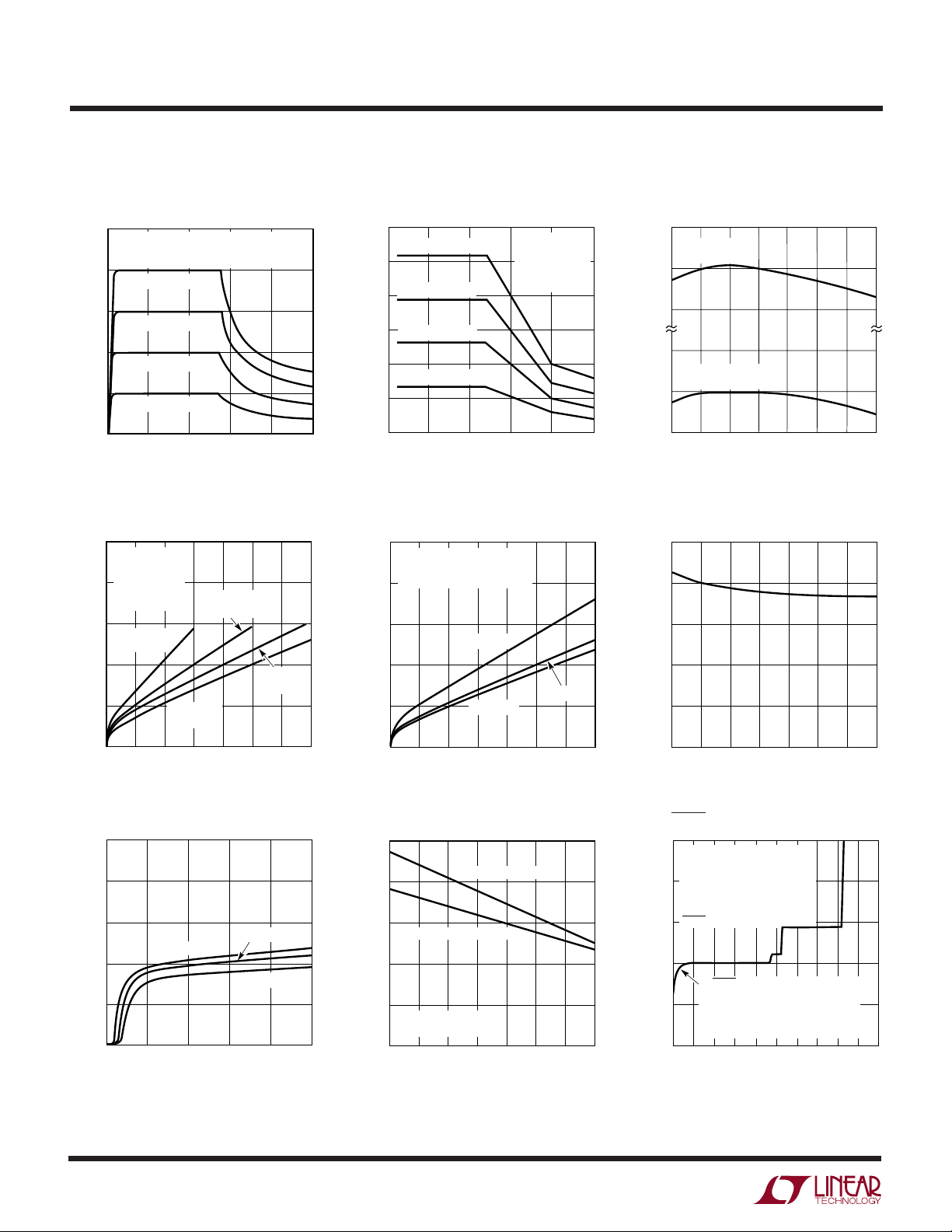
TYPICAL PERFORMANCE CHARACTERISTICS
Typical Current Limit
Characteristics
1.0
CURRENT LIMIT CHANGES ONLY SLIGHTLY
WITH TEMPERATURE SO CURVES ARE
REPRESENTATIVE OF ALL TEMPERATURES
0.8
I
, I
TIED TO V
LIM2
0.6
0.4
CURRENT (A)
0.2
I
I
I
LIM2
LIM2
LIM4
LIM
TIED TO V
TIED TO V
, I
LIM4
IN
IN
IN
OPEN
Guaranteed Current Limit
0.6
I
, I
TIED TO V
LIM2
I
LIM4
I
LIM2
I
LIM2
LIM
TIED TO V
TIED TO V
, I
OPEN
LIM4
IN
IN
0.5
0.4
0.3
CURRENT (A)
0.2
0.1
IN
CURVES REPRESENT MINIMUM
GUARANTEED
LIMITS AT ALL
TEMPERATURES
Output Voltage Temperature Drift
5.05
OUTPUT
FIXED 5V PART
5.00
4.95
3.84
VOLTAGE (V)
FEEDBACK VOLTAGE
ADJUSTABLE PART
3.80
0
5
0
INPUT-TO-OUTPUT DIFFERENTIAL VOLTAGE (V)
15
10
Minimum Input-to-Output Voltage
1.0
TJ = 25°C
REDUCED
V
IN
UNTIL OUTPUT
0.8
VOLTAGE
DROPS 1%
0.6
I
, I
LIM2
LIM4
OPEN
0.4
0.2
INPUT-TO-OUTPUT VOLTAGE (V)
0
0
0.2
0.1
OUTPUT CURRENT (A)
I
, I
LIM2
LIM4
TIED TO V
0.3
I
LIM2
IN
TO V
0.4
TIED
IN
0.5
Shutdown Input Current
25
20
15
10
INPUT CURRENT (µA)
5
0
0
TJ = 125°C
5
10
INPUT VOLTAGE (V)
TJ = –55°C
15
20
I
LIM4
TO V
0.6
TJ = 25°C
20
TIED
IN
1175 G01
1175 G04
1175 G07
0.7
0
5101520
25
0
INPUT-TO-OUTPUT DIFFERENTIAL VOLTAGE (V)
25
1175 G02
3.76
–50
0
–25
JUNCTION TEMPERATURE (°C)
50
25
75
100
125
1175 G03
SENSE Bias Current
Minimum Input-to-Output Voltage
1.0
VIN REDUCED UNTIL OUTPUT
VOLTAGE DROPS 1%.
, I
I
0.8
0.6
0.4
0.2
INPUT-TO-OUTPUT VOLTAGE (V)
0
0
TIED TO V
LIM2
LIM4
0.2
0.1
OUTPUT CURRENT (A)
IN
TJ = 125°C
TJ = –55°C
0.3
0.4
0.5
TJ = 25°C
0.6
1175 G05
0.7
Shutdown Thresholds
2.5
2.0
1.5
1.0
THRESHOLD (V)
0.5
DEVICE IS OFF
BELOW THRESHOLD
25
0
–50
POSITIVE THRESHOLD
NEGATIVE THRESHOLD
0
–25
TEMPERATURE (°C)
5025
100
125
1175 G08
75
(Adjustable Part)
100
80
60
40
CURRENT (nA)
20
0
–50
0
–25
TEMPERATURE (°C)
25
SHDN Pin Characteristics
15
VIN = 25V
CHARACTERISTICS DO NOT
CHANGE SIGNIFICANTLY WITH
10
TEMPERATURE, SO A SINGLE
CURVE IS SHOWN. POSITIVE
CURRENT FLOWS INTO
SHDN PIN
5
0
PIN CURRENT (µA)
–10
IF SHDN PIN IS NEGATIVE WITH
RESPECT TO INPUT VOLTAGE AND
–5
INPUT VOLTAGE IS LESS THAN 15V,
NEGATIVE BREAKOVER POINT WILL
BE ABOUT 8V BELOW –V
–15
–25 –20 –10 0
SHUTDOWN TO GROUND VOLTAGE (V)
–5 10 20
50
75
IN
5
125
100
1175 G06
15
25
1175 G09
4
 Loading...