

Linear Technology LT1173 Datasheet
LT1173
Micropower
DC/DC Converter
Adjustable and Fixed 5V, 12V
EATU
F
■
Operates at Supply Voltages From 2.0V to 30V
■
Consumes Only 110µA Supply Current
■
Works in Step-Up or Step-Down Mode
■
Only Three External Components Required
■
Low Battery Detector Comparator On-Chip
■
User-Adjustable Current Limit
■
Internal 1A Power Switch
■
Fixed or Adjustable Output Voltage Versions
■
Space Saving 8-Pin MiniDIP or SO8 Package
PPLICATI
A
■
Flash Memory Vpp Generators
■
3V to 5V, 5V to 12V Converters
■
9V to 5V, 12V to 5V Converters
■
LCD Bias Generators
■
Peripherals and Add-On Cards
■
Battery Backup Supplies
■
Laptop and Palmtop Computers
■
Cellular Telephones
■
Portable Instruments
RE
S
O
U
S
DUESCRIPTIO
The LT1173 is a versatile micropower DC-DC converter.
The device requires only three external components to
deliver a fixed output of 5V or 12V. Supply voltage ranges
from 2.0V to 12V in step-up mode and to 30V in step-down
mode. The LT1173 functions equally well in step-up, stepdown or inverting applications.
The LT1173 consumes just 110µA supply current at
standby, making it ideal for applications where low quiescent current is important. The device can deliver 5V at
80mA from a 3V input in step-up mode or 5V at 200mA
from a 12V input in step-down mode.
Switch current limit can be programmed with a single
resistor. An auxiliary gain block can be configured as a low
battery detector, linear post regulator, under voltage lockout circuit or error amplifier.
For input sources of less than 2V, use the LT1073.
and LTC are registered trademarks and LT is a trademark of Linear Technology Corporation.
O
PPLICATITYPICAL
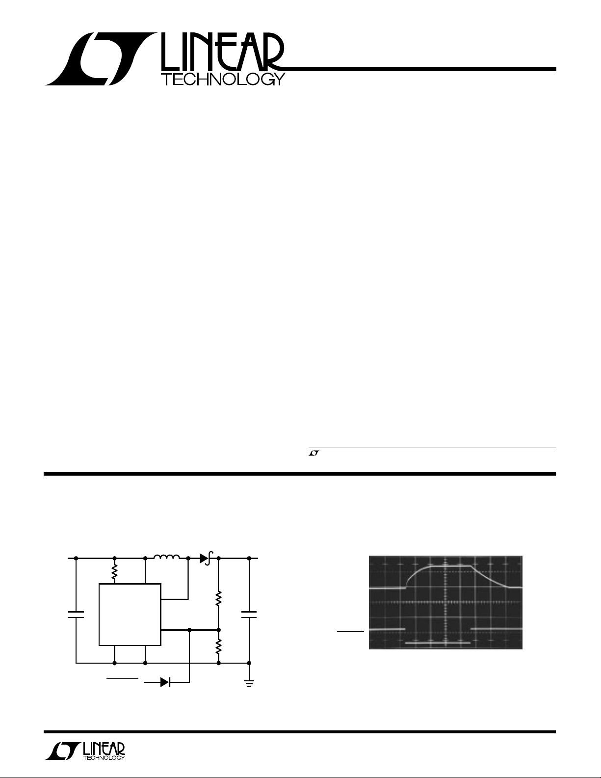
Logic Controlled Flash Memory VPP Generator
5V
IN
+
10 F
µ
*L1 = GOWANDA GA20-103K
COILTRONICS CTX100-4
NO OVERSHOOT
47Ω
V
I
LIM
GND SW2
PROGRAM
IN
LT1173
SW1
100µH
FB
1N4148
L1*
1N5818
EFFICIENCY = 81%
†
= 1% METAL FILM
U
SA
1.07M
124k
VPP Output
12V
100mA
V
OUT
5V/DIV
†
SANYO
+
OS-CON
µ
100 F
†
LT1173 • TA01
0V
PROGRAM
5V/DIV
5ms/DIV
1173 TA02
1
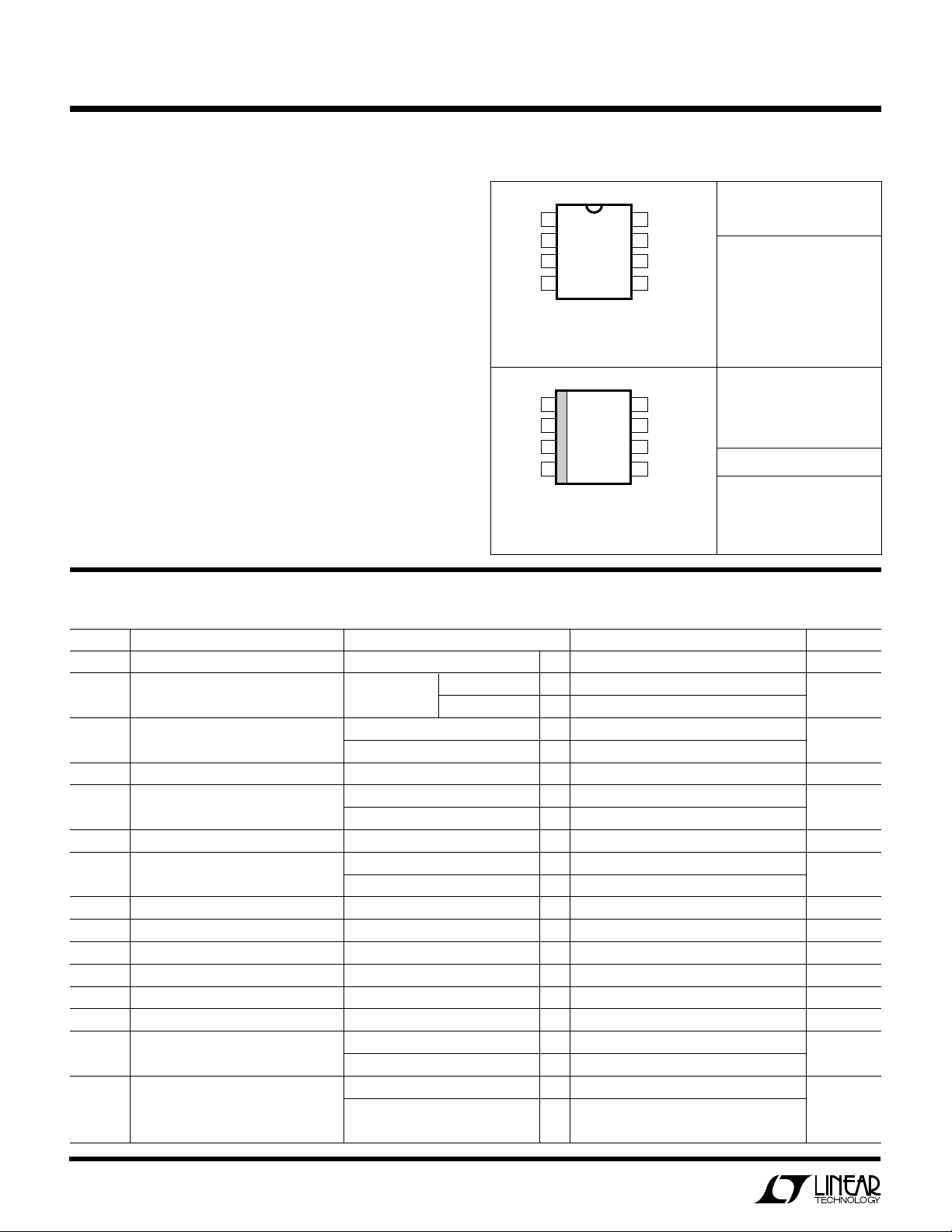
LT1173
WU
U
PACKAGE
/
O
RDER I FOR ATIO
A
W
O
LUTEXI T
S
A
WUW
ARB
U
G
I
S
Supply Voltage (VIN)................................................ 36V
SW1 Pin Voltage (V
SW2 Pin Voltage (V
) .......................................... 50V
SW1
) .............................–0.5V to V
SW2
IN
Feedback Pin Voltage (LT1173) ................................. 5V
Sense Pin Voltage (LT1173, -5, -12) ....................... 36V
Maximum Power Dissipation ............................. 500mW
Maximum Switch Current ....................................... 1.5A
Operating Temperature Range ..................... 0°C to 70°C
Storage Temperature Range .................. –65°C to 150°C
Lead Temperature, (Soldering, 10 sec.)................300°C
Consult factory for Industrial and Military grade parts
I
1
LIM
V
2
IN
SW1
3
SW2
4
N8 PACKAGE
8-LEAD PLASTIC DIP
*FIXED VERSIONS
T
= 90°C, θJA = 130°C/W
JMAX
I
1
LIM
V
2
IN
SW1
3
SW2
4
S8 PACKAGE
8-LEAD PLASTIC SOIC
*FIXED VERSIONS
T
= 90°C, θJA = 150°C/W
JMAX
TOP VIEW
TOP VIEW
FB (SENSE)*
8
SET
7
AO
6
GND
5
FB (SENSE)*
8
SET
7
AO
6
GND
5
ORDER PART
NUMBER
LT1173CN8
LT1173CN8-5
LT1173CN8-12
LT1173CS8
LT1173CS8-5
LT1173CS8-12
S8 PART MARKING
1173
11735
117312
LECTRICAL C CHARA TERIST
E
SYMBOL PARAMETER CONDITIONS MIN TYP MAX UNITS
I
I
V
V
f
t
V
V
Q
Q
IN
OUT
OSC
ON
OL
SAT
Quiescent Current Switch Off ● 110 150 µA
Quiescent Current, Boost No Load LT1173-5 135 µA
Mode Configuration
Input Voltage Step-Up Mode ● 2.0 12.6 V
Comparator Trip Point Voltage LT1173 (Note 1) ● 1.20 1.245 1.30 V
Output Sense Voltage LT1173-5 (Note 2) ● 4.75 5.00 5.25 V
Comparator Hysteresis LT1173 ● 510 mV
Output Hysteresis LT1173-5 ● 20 40 mV
Oscillator Frequency ● 18 23 30 kHz
Duty Cycle Full Load ● 43 51 59 %
Switch ON Time I
Feedback Pin Bias Current LT1173, VFB = 0V ● 10 50 nA
Set Pin Bias Current V
Gain Block Output Low I
Reference Line Regulation 2.0V ≤ VIN ≤ 5V ● 0.2 0.4 %/V
SW
Voltage, Step-Up Mode VIN = 3.0V, ISW = 650mA ● 0.5 0.65 V
SAT
ICS
TA = 25°C, VIN = 3V, unless otherwise noted.
LT1173-12 250 µA
Step-Down Mode ● 30 V
LT1173-12 (Note 2) ● 11.4 12.0 12.6 V
LT1173-12 ● 50 100 mV
tied to V
LIM
SET
SINK
5V ≤ VIN ≤ 30V ● 0.02 0.075 %/V
VIN = 5.0V, ISW = 1A 0.8 1.0 V
IN
= V
REF
= 100µA, V
= 1.00V ● 0.15 0.4 V
SET
● 17 22 32 µs
● 20 100 nA
● 1.4 V
2
LT1173
TEMPERATURE (°C)
–50
FEEDBACK PIN BIAS CURRENT ( A)
14
16
18
–25 0 25 50
LT1173 •TPC05
75
100
125
V = 3V
IN
µ
12
10
8
R ( )
10
100
SWITCH CURRENT (mA)
400
800
1200
100
LT1173 • TPC03
Ω
1000
900
700
600
500
300
200
LIM
1000
1100
2V ≤ VIN ≤ 5V
LECTRICAL C CHARA TERIST
E
ICS
TA = 25°C, V
= 3V, unless otherwise noted.
IN
SYMBOL PARAMETER CONDITIONS MIN TYP MAX UNITS
V
SAT
A
V
SW
Voltage, Step-Down Mode VIN = 12V, ISW = 650mA 1.1 1.5 V
SAT
● 1.7 V
Gain Block Gain RL = 100kΩ (Note 3) ● 400 1000 V/V
Current Limit 220Ω to I
LIM
to V
IN
400 mA
Current Limit Temperature Coeff. ● –0.3 %/°C
Switch OFF Leakage Current Measured at SW1 Pin 1 10 µA
V
SW2
The ● denotes the specifications which apply over the full operating
temperature range.
Note 1: This specification guarantees that both the high and low trip points
of the comparator fall within the 1.20V to 1.30V range.
Maximum Excursion Below GND I
≤ 10µA, Switch Off –400 –350 mV
SW1
Note 2: The output voltage waveform will exhibit a sawtooth shape due to
the comparator hysteresis. The output voltage on the fixed output versions
will always be within the specified range.
Note 3: 100kΩ resistor connected between a 5V source and the AO pin.
UW
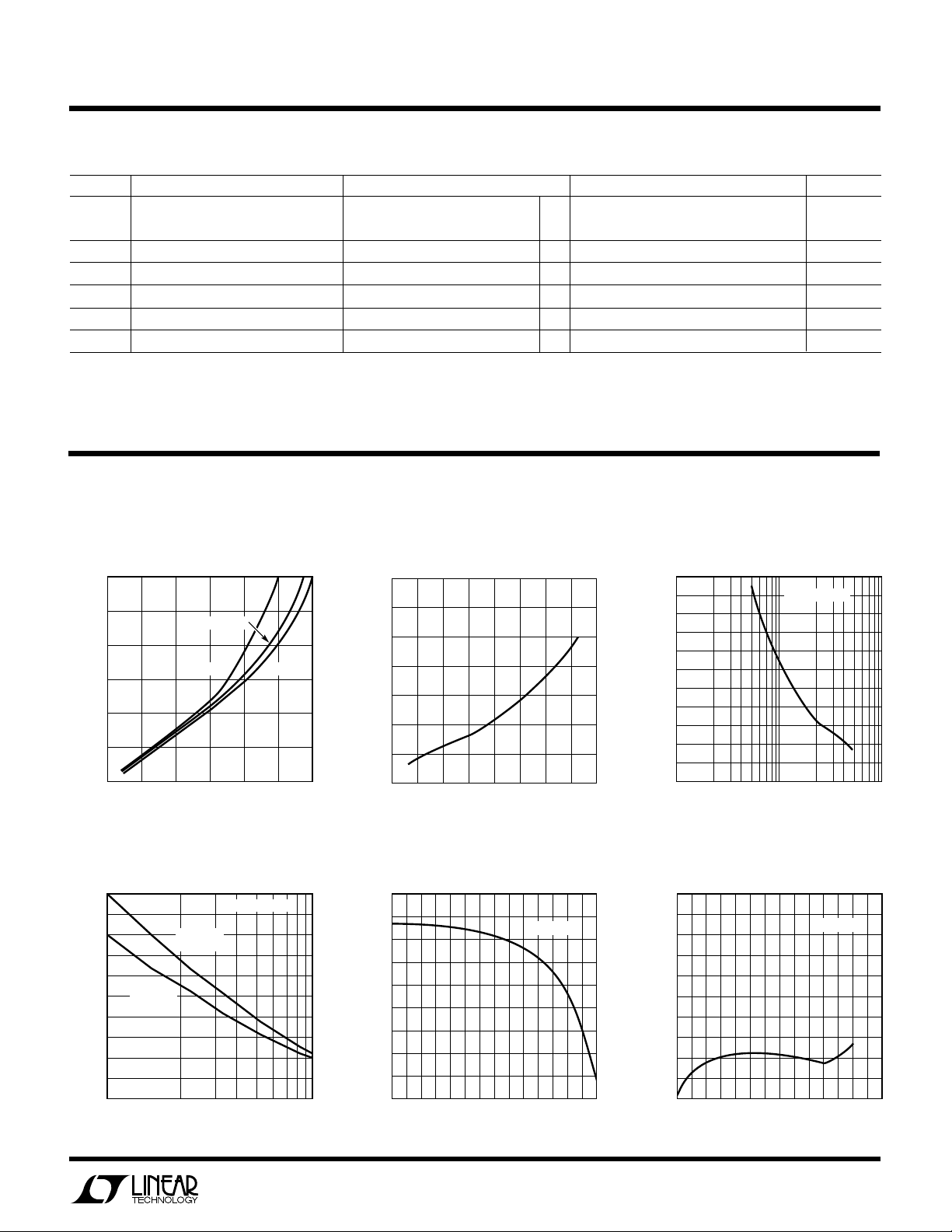
Y
PICA
1.2
LPER
F
O
R
AT
CCHARA TERIST
E
C
ICS
Switch ON Voltage
Saturation Voltage Step-Up Mode Step-Down Mode Maximum Switch Current vs
(SW2 Pin Grounded) (SW1 Pin Connected to VIN)R
1.4
Step-Up Mode
LIM
1.0
0.8
0.6
CESAT
V (V)
0.4
0.2
0
0
0.2 0.4 0.6 0.8
Maximum Switch Current vs Set Pin Bias Current vs Feedback Pin Bias Current vs
R
Step-Down Mode Temperature Temperature
LIM
1000
900
800
700
600
500
400
300
SWITCH CURRENT (mA)
200
100
0
100
= 12V
V
IN
L = 250µH
V = 3.0V
V = 2.0V
IN
I (A)
SWITCH
VIN = 24V
L = 500µH
R ( )
LIM
1.3
IN
V = 5.0V
IN
1.0 1.2
LT1173 • TPC01
V
= 5V
OUT
1000
Ω
LT1173 • TPC09
1.2
1.1
1.0
0.9
SWITCH ON VOLTAGE (V)
0.8
0.7
0.1 0.2 0.3 0.4
0
I (A)
SWITCH
20
15
10
SET PIN BIAS CURRENT (nA)
5
–25 0 25 50
–50
TEMPERATURE (°C)
0.5 0.6
V = 3V
IN
75
0.7 0.8
LT1173 • TPC02
100
LT1173 •TPC04
125
3
LT1173
VIN(V)
0
22.0
F
OSC
(kHz)
22.5
23.0
23.5
24.5
25.0
5101520
LT1173 • TPC08
24.0
25 30
25.5
26.0
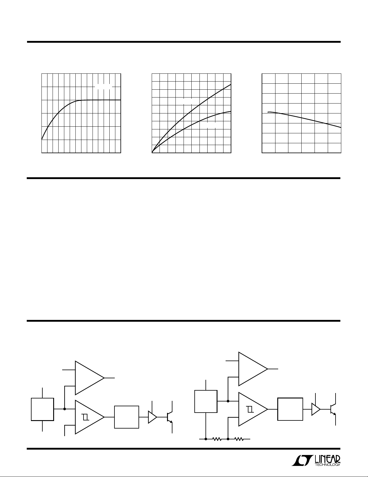
UW
Y
PICA
120
LPER
F
O
R
AT
CCHARA TERIST
E
C
ICS
Quiescent Current vs Temperature Supply Current vs Switch Current Oscillator Frequency
50
V = 3V
IN
40
110
µ
IN
I ( A)
100
90
–25 0 25 50
–50
TEMPERATURE (°C)
U
PI
I
FUUC
(Pin 1): Connect this pin to VIN for normal use. Where
LIM
TI
O
U
S
75
100
LT1173 •TPC06
125
30
20
SUPPLY CURRENT (mA)
10
0
0
V = 5V
200
400 600 800
SWITCH CURRENT (mA)
lower current limit is desired, connect a resistor between
I
and VIN. A 220Ω resistor will limit the switch current
LIM
to approximately 400mA.
V
(Pin 2): Input supply voltage.
IN
SW1 (Pin 3): Collector of power transistor. For step-up
mode connect to inductor/diode. For step-down mode
connect to VIN.
SW2 (Pin 4): Emitter of power transistor. For step-up
mode connect to ground. For step-down mode connect to
inductor/diode. This pin must never be allowed to go more
than a Schottky diode drop below ground.
IN
V = 2V
IN
1000
LT1173 •TPC07
GND (Pin 5): Ground.
AO (Pin 6): Auxiliary Gain Block (GB) output. Open collec-
tor, can sink 100µA.
SET (Pin 7): GB input. GB is an op amp with positive input
connected to SET pin and negative input connected to
1.245V reference.
FB/SENSE (Pin 8): On the LT1173 (adjustable) this pin
goes to the comparator input. On the LT1173-5 and
LT1173-12, this pin goes to the internal application resistor that sets output voltage.
BLOCK
V
IN
1.245V
REFERENCE
GND
4
SET
IDAGRA
A2
GAIN BLOCK/
ERROR AMP
COMPARATOR
FB
LT1173
A1
W
S
AO
OSCILLATOR
I
LIM
DRIVER
SW1
SW2
LT1173 • BD01
REFERENCE
GND
V
IN
1.245V
R1
SET
R2
753k
A2
GAIN BLOCK/
ERROR AMP
Ω
LT1173-5, -12
A1
COMPARATOR
SENSE
LT1173-12:
AO
OSCILLATOR
LT1173-5:
I
DRIVER
R1 = 250k
R1 = 87.4k
LIM
Ω
Ω
SW1
SW2
LT1173 • BD02

LT1173 OPER
I
VV
IN
=
−
()
21
10001Ω
AT
LT1173
U
O
I
The LT1173 is a gated oscillator switcher. This type architecture has very low supply current because the switch is
cycled only when the feedback pin voltage drops below the
reference voltage. Circuit operation can best be understood by referring to the LT1173 block diagram. Comparator A1 compares the feedback pin voltage with the 1.245V
reference voltage. When feedback drops below 1.245V, A1
switches on the 24kHz oscillator. The driver amplifier
boosts the signal level to drive the output NPN power
switch. An adaptive base drive circuit senses switch
current and provides just enough base drive to ensure
switch saturation without overdriving the switch, resulting
in higher efficiency. The switch cycling action raises the
output voltage and feedback pin voltage. When the feedback voltage is sufficient to trip A1, the oscillator is gated
off. A small amount of hysteresis built into A1 ensures loop
stability without external frequency compensation. When
the comparator is low the oscillator and all high current
circuitry is turned off, lowering device quiescent current
to just 110µA, for the reference, A1 and A2.
The oscillator is set internally for 23µs ON time and 19µs
OFF time, optimizing the device for circuits where V
and VIN differ by roughly a factor of 2. Examples include a
3V to 5V step-up converter or a 9V to 5V step-down
converter.
OUT
A2 is a versatile gain block that can serve as a low battery
detector, a linear post regulator, or drive an under voltage
lockout circuit. The negative input of A2 is internally
connected to the 1.245V reference. A resistor divider from
VIN to GND, with the mid-point connected to the SET pin
provides the trip voltage in a low battery detector application. The gain block output (AO) can sink 100µA (use a 47k
resistor pull-up to +5V). This line can signal a microcontroller that the battery voltage has dropped below the
preset level.
A resistor connected between the I
maximum switch current. When the switch current exceeds the set value, the switch cycle is prematurely
terminated. If current limit is not used, I
directly to VIN. Propagation delay through the current limit
circuitry is approximately 2µs.
In step-up mode the switch emitter (SW2) is connected to
ground and the switch collector (SW1) drives the inductor; in step-down mode the collector is connected to V
and the emitter drives the inductor.
The LT1173-5 and LT1173-12 are functionally identical to
the LT1173. The -5 and -12 versions have on-chip voltage
setting resistors for fixed 5V or 12V outputs. Pin 8 on the
fixed versions should be connected to the output. No
external resistors are needed.
pin and VIN sets
LIM
should be tied
LIM
IN
U
O
PPLICATI
A
Measuring Input Current at Zero or Light Load
Obtaining meaningful numbers for quiescent current and
efficiency at low output current involves understanding
how the LT1173 operates. At very low or zero load current,
the device is idling for seconds at a time. When the output
voltage falls enough to trip the comparator, the power
switch comes on for a few cycles until the output voltage
rises sufficiently to overcome the comparator hysteresis.
When the power switch is on, inductor current builds up
to hundreds of milliamperes. Ordinary digital multimeters
are not capable of measuring average current because of
bandwidth and dynamic range limitations. A different
S
I FOR ATIO
WU
U
approach is required to measure the 100µA off-state and
500mA on-state currents of the circuit.
Quiescent current can be accurately measured using the
circuit in Figure 1. V
LT1173. The circuit must be “booted” by shorting V2 to
V
. After the LT1173 output voltage has settled, discon-
SET
nect the short. Input voltage is V2, and average input
current can be calculated by this formula:
is set to the input voltage of the
SET
5
 Loading...