

Linear Technology LT1168 Datasheet
LT1168
Final Electrical Specifications
Low Power, Single
Resistor Gain Programmable, Micropower
FEATURES
■
Supply Current: 530µA Max
■
Meets IEC 1000-4-2 Level 4 ESD Tests with
Two External 5k Resistors
■
Single Gain Set Resistor: G = 1 to 10,000
■
Gain Error: G = 10, 0.4% Max
■
Input Offset Voltage Drift: 0.3µV/°C Max
■
Gain Nonlinearity: G = 10, 20ppm Max
■
Input Offset Voltage: 40µV Max
■
Input Bias Current: 250pA Max
■
PSRR at AV =1: 103dB Min
■
CMRR at AV = 1: 90dB Min
■
Wide Supply Range: ±2.3V to ±18V
■
1kHz Voltage Noise: 10nV/√Hz
■
0.1Hz to 10Hz Noise: 0.28µV
■
Available in 8-Pin PDIP and SO Packages
P-P
U
APPLICATIO S
■
Bridge Amplifiers
■
Strain Gauge Amplifiers
■
Thermocouple Amplifiers
■
Differential to Single-Ended Converters
■
Differential Voltage to Current Converters
■
Data Acquisition
■
Battery-Powered and Portable Equipment
■
Medical Instrumentation
■
Scales
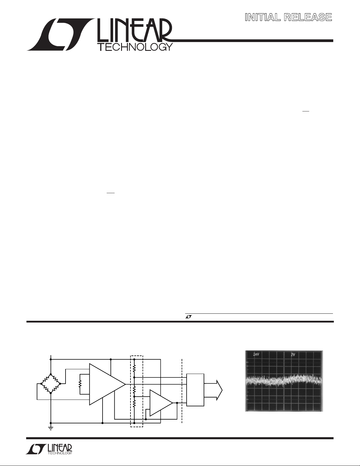
Precision Instrumentation Amplifier
DESCRIPTIO
U
March 2000
The LT®1168 is a micropower, precision instrumentation
amplifier that requires only one external resistor to set gains
of 1 to 10,000. The low voltage noise of 10nV/√Hz (at 1kHz)
is not compromised by low power dissipation (350µA typical
for ±15V supplies). The wide supply range of ±2.3V to ±18V
allows the LT1168 to fit into a wide variety of industrial as well
as battery-powered applications.
The high accuracy of the LT1168 is due to a 20ppm maximum
nonlinearity and 0.4% max gain error (G = 10). Previous
monolithic instrumentation amps cannot handle a 2k load
resistor whereas the nonlinearity of the LT1168 is specified
for loads as low as 2k. The LT1168 is laser trimmed for very
low input offset voltage (40µV max), drift (0.3µV/°C), high
CMRR (90dB, G = 1) and PSRR (103dB, G = 1). Low input
bias currents of 250pA max are achieved with the use of
superbeta processing. The output can handle capacitive
loads up to 1000pF in any gain configuration while the inputs
are ESD protected up to 13kV (human body). The LT1168
with two external 5k resistors passes the IEC 1000-4-2 level
4 specification.
The LT1168 is a pin-for-pin improved second source for the
AD620 and INA118. The LT1168, offered in 8-pin PDIP and
SO packages, requires significantly less PC board area than
discrete op amp resistor designs. These advantages make
the LT1168 the most cost effective solution for precision
instrumentation amplifier applications.
, LTC and LT are registered trademarks of Linear Technology Corporation.
TYPICAL APPLICATIO
5V
1
3.5k
3.5k
*See Theory of Operation section
3.5k
G = 200
3.5k
249Ω
3
8
R1
1
2
U
Single Supply* Pressure Monitor
+
LT1168
–
4
Information furnished by Linear Technology Corporation is believed to be accurate and reliable.
However, no responsibility is assumed for its use. Linear Technology Corporation makes no representation that the interconnection of its circuits as described herein will not infringe on existing patent rights.
BI TECHNOLOGIES
67-8-3 R40KQ, (0.02% RATIO MATCH)
7
5
40k
6
20k
3
+
40k
1/2
LT1112
2
–
REF
IN
1
AGND
LTC
ADC
®
1286
DIGITAL
DATA
OUTPUT
1168 TA01
Gain Nonlinearity
NONLINEARITY (100ppm/DIV)
G = 1000 OUTPUT VOLTAGE (2V/DIV)
RL = 2K
V
= ±10V
OUT
1168 TA01a
1
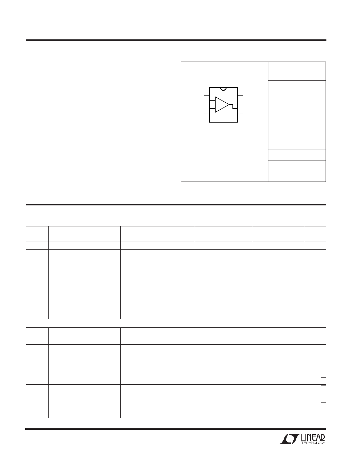
LT1168
1
2
3
4
8
7
6
5
TOP VIEW
R
G
–IN
+IN
–V
S
R
G
+V
S
OUTPUT
REF
N8 PACKAGE
8-LEAD PDIP
S8 PACKAGE
8-LEAD PLASTIC SO
+
–
WW
W
U
ABSOLUTE MAXIMUM RATINGS
(Note 1)
Supply Voltage ...................................................... ±20V
Differential Input Voltage (Within the
Supply Voltage) ..................................................... ±40V
Input Voltage (Equal to Supply Voltage) ................±20V
Input Current (Note 2) ....................................... ±20mA
Output Short-Circuit Duration (Note 3)............ Indefinite
Operating Temperature Range (Note 4) .. – 40°C to 85°C
Specified Temperature Range
LT1168AC/LT1168C (Note 5) ............. – 40°C to 85°C
LT1168AI/LT1168I ............................. –40°C to 85°C
Storage Temperature Range ................. –40°C to 150°C
Lead Temperature (Soldering, 10 sec).................. 300°C
U
W
PACKAGE/ORDER INFORMATION
ORDER PART
NUMBER
LT1168ACN8
LT1168ACS8
LT1168AIN8
LT1168AIS8
LT1168CN8
LT1168CS8
LT1168IN8
LT1168IS8
T
= 150°C, θJA = 130°C/ W (N8)
JMAX
= 150°C, θJA = 190°C/W (S8)
T
JMAX
Consult factory for Military grade parts.
S8 PART MARKING
1168A
1168AI
1168
1168I
U
ELECTRICAL CHARACTERISTICS
SYMBOL PARAMETER CONDITIONS (Note 6) MIN TYP MAX MIN TYP MAX UNITS
G Gain Range G = 1 + (49.4k/RG) 1 10k 1 10k
Gain Error G = 1 0.008 0.02 0.015 0.03 %
G = 10 (Note 7) 0.04 0.4 0.05 0.5 %
G = 100 (Note 7) 0.04 0.5 0.05 0.6 %
G = 1000 (Note 7) 0.08 0.5 0.08 0.6 %
Gain Nonlinearity (Notes 7, 8) VO = ±10V, G = 1 2 6 3 10 ppm
V
= ±10V,G = 10 and 100 10 20 15 25 ppm
O
= ±10V, G = 1000 20 40 25 60 ppm
V
O
VO = ±10V, G = 1, RL = 2k 4 15 5 20 ppm
= ±10V,G = 10 and 100, RL = 2k 20 40 30 60 ppm
V
O
= ±10V, G = 1000, RL = 2k 40 75 50 90 ppm
V
O
V
OST
V
OSI
V
OSO
I
OS
I
B
e
n
i
n
R
IN
2
Total Input Referred Offset Voltage V
Input Offset Voltage G = 1000, VS = ±5V to ±15V 15 40 20 60 µV
Output Offset Voltage G = 1, VS = ±5V to ±15V 40 200 50 300 µV
Input Offset Current 90 300 100 450 pA
Input Bias Current 40 250 80 500 pA
Input Noise Voltage, RTI 0.1Hz to 10Hz, G = 1 2.00 2.00 µV
Input Noise Voltage Density, RTI fO = 1kHz 10 15 10 15 nV/√Hz
Output Noise Voltage Density, RTI fO = 1kHz (Note 9) 165 220 165 220 nV/√Hz
Input Noise Current fO = 0.1Hz to 10Hz 5 5 pA
Input Noise Current Density fO = 10Hz 74 74 fA/√Hz
Input Resistance VIN = ±10V 300 1000 200 1000 GΩ
= V
OST
0.1Hz to 10Hz, G = 1000 0.28 0.28 µV
TA = 25°C. VS = ±15V, VCM = 0V, RL = 10k unless otherwise noted.
LT1168AC/LT1168AI LT1168C/LT1168I
+ V
OSO
/G
OSI
P-P
P-P
P-P
LT1168
ELECTRICAL CHARACTERISTICS
SYMBOL PARAMETER CONDITIONS (Note 6) MIN TYP MAX MIN TYP MAX UNITS
C
IN(DIFF)
C
IN(CM)
V
CM
CMRR Common Mode 1k Source Imbalance,
PSRR Power Supply VS = ±2.3V to ±18V
I
S
V
OUT
I
OUT
BW Bandwidth G = 1 400 400 kHz
SR Slew Rate G = 1, V
REFIN Reference Input Resistance 60 60 kΩ
I
REFIN
V
REF
A
VREF
Differential Input Capacitance fO = 100kHz 1.6 1.6 pF
Common Mode Input fO = 100kHz 1.6 1.6 pF
Capacitance
Input Voltage Range G = 1, Other Input Grounded
= ±2.3V to ±5V –VS + 1.9 +VS – 1.2 –VS + 1.9 +VS – 1.2 V
V
S
V
= ±5V to ±18V –VS + 1.9 +VS – 1.4 –VS + 1.9 +VS – 1.4 V
S
Rejection Ratio V
Rejection Ratio G = 1 103 108 100 108 dB
Supply Current VS = ±2.3V to ±18V 350 530 350 530 µA
Output Voltage Swing RL = 10k
Output Current 20 27 20 27 mA
Settling Time to 0.01% 10V Step
Reference Input Current V
Reference Voltage Range –VS + 1.6 +VS – 1.6 –VS + 1.6 +VS – 1.6 V
Reference Gain to Output 1 ± 0.0001 1 ± 0.0001
= 0V to ±10V
CM
G = 1 90 95 85 95 dB
G = 10 106 115 100 115 dB
G = 100 120 135 110 135 dB
G = 1000 126 140 120 140 dB
G = 10 122 128 118 128 dB
G = 100 131 145 126 145 dB
G = 1000 135 150 130 150 dB
V
= ±2.3V to ±5V –VS + 1.1 +VS – 1.2 –VS + 1.1 +VS – 1.2 V
S
= ±5V to ±18V –VS + 1.2 +VS – 1.3 –VS + 1.2 +VS – 1.3 V
V
S
G = 10 200 200 kHz
G = 100 13 13 kHz
G = 1000 1 1 kHz
OUT
G = 1 to 100 30 30 µs
G = 1000 200 200 µs
= 0V 18 18 µA
REF
TA = 25°C. VS = ±15V, VCM = 0V, RL = 10k unless otherwise noted.
LT1168AC/LT1168AI LT1168C/LT1168I
= ±10V 0.3 0.5 0.3 0.5 V/µs
The ● denotes the specifications which apply over the 0°C ≤ TA ≤ 70°C temperature range. VS = ±15V, VCM = 0V, RL = 10k unless
otherwise noted.
LT1168AC LT1168C
SYMBOL PARAMETER CONDITIONS (Note 6) MIN TYP MAX MIN TYP MAX UNITS
Gain Error G = 1 ● 0.01 0.03 0.012 0.04 %
G = 10 (Note 7)
G = 100 (Note 7)
G = 1000 (Note 7)
Gain Nonlinearity V
(Notes 7, 8) V
G/T Gain vs Temperature G < 1000 (Note 7) ● 100 200 100 200 ppm/°C
= ±10V, G = 1 ● 2 15 3 20 ppm
OUT
= ±10V, G = 10 and 100 ● 7 30 10 35 ppm
OUT
= ±10V, G = 1000 ● 25 60 30 80 ppm
V
OUT
● 0.40 1.5 0.500 1.6 %
● 0.45 1.6 0.550 1.7 %
● 0.50 1.7 0.600 1.8 %
3
LT1168
ELECTRICAL CHARACTERISTICS
The ● denotes the specifications which apply over the 0°C ≤ TA ≤ 70°C
temperature range. VS = ±15V, VCM = 0V, RL = 10k unless otherwise noted.
LT1168AC LT1168C
SYMBOL PARAMETER CONDITIONS (Note 6) MIN TYP MAX MIN TYP MAX UNITS
V
OST
V
OSI
V
OSIH
V
OSO
V
OSOH
V
OSI
V
OSO
I
OS
IOS/T Input Offset Current Drift ● 0.3 0.4 pA/°C
I
B
IB/T Input Bias Current Drift ● 1.4 1.4 pA/°C
V
CM
CMRR Common Mode 1k Source Imbalance,
PSRR Power Supply VS = ±2.3V to ±18V
I
S
V
OUT
I
OUT
SR Slew Rate G = 1, V
V
REF
Total Input Referred Offset Voltage V
OST
= V
OSI
+ V
OSO
/G
Input Offset Voltage VS = ±5V to ±15V ● 18 60 23 80 µV
Input Offset Voltage Hysteresis (Notes 7, 10) ● 3.0 3.0 µV
Output Offset Voltage VS = ±5V to ±15V ● 60 380 70 500 µV
Output Offset Voltage Hysteresis (Notes 7, 10) ● 30 30 µV
/T Input Offset Drift (RTI) (Note 9) ● 0.05 0.3 0.06 0.4 µV/°C
/T Output Offset Drift (Note 9) ● 0.7 3 0.8 4 µV/°C
Input Offset Current ● 100 400 120 550 pA
Input Bias Current ● 65 350 105 600 pA
Input Voltage Range G = 1, Other Input Grounded
V
= ±2.3V to ±5V ● –VS + 2.1 +VS – 1.3 –VS + 2.1 +VS – 1.3 V
S
= ±5V to ±18V ● –VS + 2.1 +VS – 1.4 –VS + 2.1 +VS – 1.4 V
V
S
Rejection Ratio V
Rejection Ratio G = 1
= 0V to ±10V
CM
G = 1
G = 10
G = 100
G = 1000
G = 10
G = 100
G = 1000
● 88 92 83 92 dB
● 100 110 97 110 dB
● 115 120 113 120 dB
● 117 135 114 135 dB
● 102 115 98 115 dB
● 123 130 118 130 dB
● 127 135 124 135 dB
● 129 145 126 145 dB
Supply Current VS = ±2.3V to ±18V ● 390 615 390 615 µA
Output Voltage Swing RL = 10k
= ±2.3V to ±5V ● –VS + 1.4 +VS – 1.3 –VS + 1.4 +VS – 1.3 V
V
S
V
= ±5V to ±18V ● –VS + 1.6 +VS – 1.5 –VS + 1.6 +VS – 1.5 V
S
Output Current ● 16 21 16 21 mA
= ±10V ● 0.25 0.48 0.25 0.48 V/µs
OUT
Voltage Range (Note 9) ● –VS + 1.6 +VS – 1.6 –VS + 1.6 +VS – 1.6 V
The ● denotes the specifications which apply over the –40°C ≤ TA ≤ 85°C temperature range. VS = ±15V, VCM = 0V, RL = 10k unless
otherwise noted. (Note 8)
LT1168AI LT1168I
SYMBOL PARAMETER CONDITIONS (Note 6) MIN TYP MAX MIN TYP MAX UNITS
Gain Error G = 1 ● 0.014 0.04 0.015 0.05 %
G = 10 (Note 7)
G = 100 (Note 7)
G = 1000 (Note 7)
G
N
Gain Nonlinearity VO = ±10V, G = 1 ● 3 20 5 25 ppm
(Notes 7, 8) V
= ±10V, G = 10 and 100 ● 10 35 15 40 ppm
O
VO = ±10V, G = 1000
● 0.600 1.9 0.700 2.0 %
● 0.600 2.0 0.700 2.1 %
● 0.600 2.1 0.700 2.2 %
● 30 70 35 100 ppm
G/T Gain vs Temperature G < 1000 (Note 7) ● 100 200 100 200 ppm/°C
4
LT1168
ELECTRICAL CHARACTERISTICS
The ● denotes the specifications which apply over the –40°C ≤ TA ≤ 85°C temperature range. VS = ±15V, VCM = 0V, RL = 10k unless
otherwise noted. (Note 5)
LT1168AI LT1168I
SYMBOL PARAMETER CONDITIONS (Note 6) MIN TYP MAX MIN TYP MAX UNITS
V
OST
V
OSI
V
OSIH
V
OSO
V
OSOH
V
OSI
V
OSO
I
OS
IOS/T Input Offset Current Drift ● 0.3 0.3 pA/°C
I
B
IB/T Input Bias Current Drift ● 1.4 1.4 pA/°C
V
CM
CMRR Common Mode 1k Source Imbalance,
PSRR Power Supply VS = ±2.3V to ±18V
I
S
V
OUT
I
OUT
SR Slew Rate ● 0.22 0.41 0.22 0.42 V/µs
V
REF
Note 1: Absolute Maximum Ratings are those values beyond which the life
of a device may be imparied.
Note 2: If the input voltage exceeds the supplies, the input current should
be limited to less than 20mA.
Note 3: A heat sink may be required to keep the junction temperature
below absolute maximum.
Note 4: The LT1168AC/LT1168C are guaranteed functional over the
operating temperature range of –40°C and 85°C.
Note 5: The LT1168AC/LT1168C are guaranteed to meet specified
performance from 0°C to 70°C. The LT1168AC/LT1168C are designed,
characterized and expected to meet specified performance from –40°C
and 85°C but are not tested or QA sampled at these temperatures. The
LT1168AI/LT1168I are guaranteed to meet specified performance from
–40°C to 85°C.
Total Input Referred Offset Voltage V
OST
= V
OSI
+ V
OSO
/G
Input Offset Voltage ● 20 75 25 100 µV
Input Offset Voltage Hysteresis (Notes 7, 10) ● 3.0 3.0 µV
Output Offset Voltage ● 180 500 200 600 µV
Output Offset Voltage Hysteresis (Notes 7, 10) ● 30 30 µV
/T Input Offset Drift (RTI) (Note 9) ● 0.05 0.3 0.06 0.4 µV/°C
/T Output Offset Drift (Note 9) ● 0.8 5 1 6 µV/°C
Input Offset Current ● 110 550 120 700 pA
Input Bias Current ● 120 500 220 800 pA
Input Voltage Range VS = ±2.3V to ±5V ● –VS + 2.1 +VS – 1.3 –VS + 2.1 +VS – 1.3 V
V
= ±5V to ±18V ● –VS + 2.1 +VS – 1.4 –VS + 2.1 +VS – 1.4 V
S
Rejection Ratio V
Rejection Ratio G = 1
= 0V to ±10V
CM
G = 1
G = 10
G = 100
G = 1000
G = 10
G = 100
G = 1000
● 86 90 81 90 dB
● 98 105 95 105 dB
● 114 118 112 118 dB
● 116 133 112 133 dB
● 100 112 95 112 dB
● 120 125 115 125 dB
● 125 132 120 132 dB
● 128 140 125 140 dB
Supply Current ● 420 650 420 650 µA
Output Voltage Swing VS = ±2.3V to ±5V ● –VS + 1.4 +VS – 1.3 –VS + 1.4 +VS – 1.3 V
V
= ±5V to ±18V ● –VS + 1.6 +VS – 1.5 –VS + 1.6 +VS – 1.5 V
S
Output Current ● 15 20 15 20 mA
Voltage Range (Note 9) ● –VS + 1.6 +VS – 1.6 –VS + 1.6 +VS – 1.6 V
Note 6: Typical parameters are defined as the 60% of the yield parameter
distribution.
Note 7: Does not include the tolerance of the external gain resistor RG.
Note 8: This parameter is measured in a high speed automatic tester that
does not measure the thermal effects with longer time constants. The
magnitude of these thermal effects are dependent on the package used,
heat sinking and air flow conditions.
Note 9: This parameter is not 100% tested.
Note 10: Hysteresis in offset voltage is created by package stress that
differs depending on whether the IC was previously at a higher or lower
temperature. Offset voltage hysteresis is always measured at 25°C, but
the IC is cycled to 85°C I-grade (or 70°C C-grade) or –40°C I-grade
(0°C C-grade) before successive measurement. 60% of the parts will
pass the typical limit on the data sheet.
5
 Loading...