

Linear Technology LT1167 Datasheet
FEATURES
■
Single Gain Set Resistor: G = 1 to 10,000
■
Gain Error: G = 10, 0.08% Max
■
Gain Nonlinearity: G = 10, 10ppm Max
■
Input Offset Voltage: G = 10, 60µV Max
■
Input Offset Voltage Drift: 0.3µV/°C Max
■
Input Bias Current: 350pA Max
■
PSRR at G = 1: 105dB Min
■
CMRR at G = 1: 90dB Min
■
Supply Current: 1.3mA Max
■
Wide Supply Range: ±2.3V to ±18V
■
1kHz Voltage Noise: 7.5nV/√Hz
■
0.1Hz to 10Hz Noise: 0.28µV
■
Available in 8-Pin PDIP and SO Packages
■
Meets IEC 1000-4-2 Level 4 ESD Tests with
P-P
Two External 5k Resistors
U
APPLICATIONS
■
Bridge Amplifiers
■
Strain Gauge Amplifiers
■
Thermocouple Amplifiers
■
Differential to Single-Ended Converters
■
Medical Instrumentation
LT1167
Single Resistor Gain
Programmable, Precision
Instrumentation Amplifier
U
DESCRIPTION
The LT®1167 is a low power, precision instrumentation
amplifier that requires only one external resistor to set gains
of 1 to 10,000. The low voltage noise of 7.5nV/√Hz (at 1kHz)
is not compromised by low power dissipation (0.9mA typical
for ±2.3V to ±15V supplies).
The high accuracy of 10ppm maximum nonlinearity and
0.08% max gain error (G = 10) is not degraded even for load
resistors as low as 2k (previous monolithic instrumentation
amps used 10k for their nonlinearity specifications). The
LT1167 is laser trimmed for very low input offset voltage
(40µV max), drift (0.3µ V/°C), high CMRR (90dB, G = 1) and
PSRR (105dB, G = 1). Low input bias currents of 350pA max
are achieved with the use of superbeta processing. The
output can handle capacitive loads up to 1000pF in any gain
configuration while the inputs are ESD protected up to 13kV
(human body). The LT1167 with two external 5k resistors
passes the IEC 1000-4-2 level 4 specification.
The LT1167, offered in 8-pin PDIP and SO packages, requires
significantly less PC board area than discrete multi op amp
and resistor designs. These advantages make the LT1167 the
most cost effective solution for precision instrumentation
amplifier applications.
, LTC and LT are registered trademarks of Linear Technology Corporation.
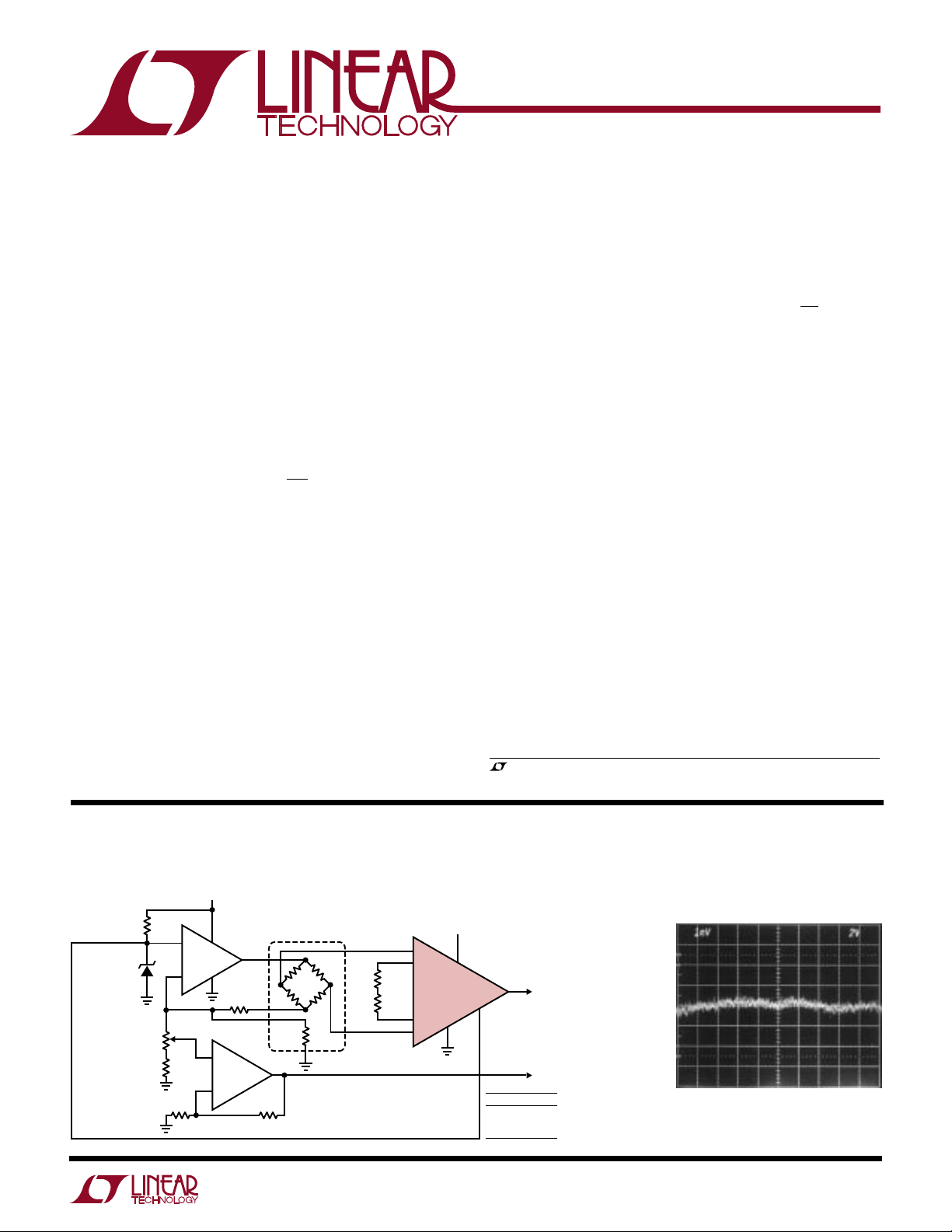
TYPICAL APPLICATION
Single Supply Barometer
V
S
LT1634CCZ-1.25
392k
R5
3
8
+
2
R8
100k
–
1/2
LT1490
5
6
4
+
LT1490
–
50k
50k
1
2
R4
R3
1
R6
1k
1/2
LUCAS NOVA SENOR
NPC-1220-015-A-3L
4
5k
5k
2
6
R
SET
5
7
R7
50k
U
1
–
5k
5k
+
R1
825Ω
R2
12Ω
3
0.2% ACCURACY AT 25°C
1.2% ACCURACY AT 0°C TO 60°C
= 8V TO 30V
V
S
Gain Nonlinearity
V
S
–
2
1
8
3
7
5
VOLTS
2.800
3.000
3.200
6
INCHES Hg
TO
4-DIGIT
DVM
28.00
30.00
32.00
1167 TA01
NONLINEARITY (100ppm/DIV)
G = 1000
R
= 1k
L
V
OUT
OUTPUT VOLTAGE (2V/DIV)
= ±10V
1167 TA02
LT1167
G = 60
+
4
1
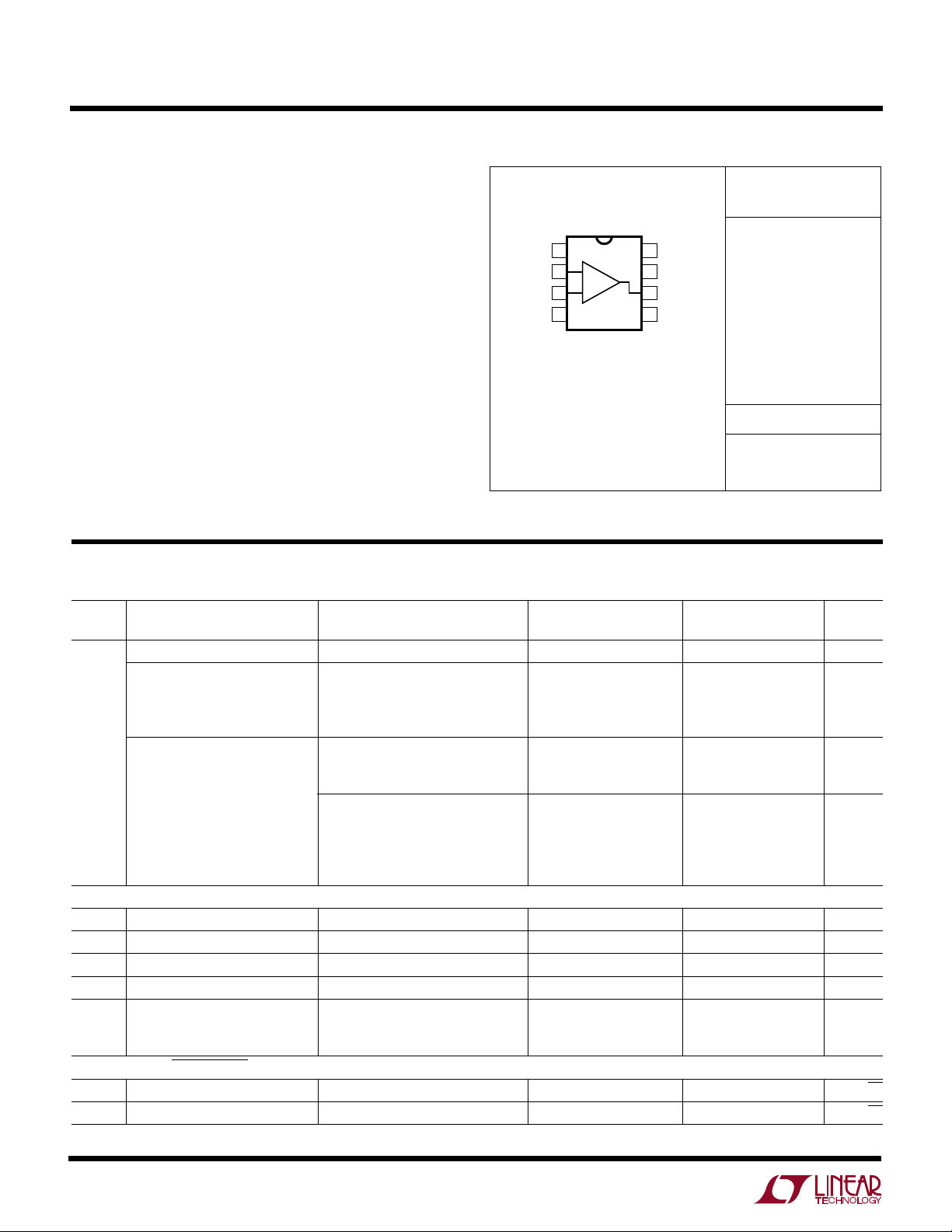
LT1167
1
2
3
4
8
7
6
5
TOP VIEW
R
G
–IN
+IN
–V
S
RG
+V
S
OUTPUT
REF
N8 PACKAGE
8-LEAD PDIP
S8 PACKAGE
8-LEAD PLASTIC SO
+
–
WW
W
U
ABSOLUTE MAXIMUM RATINGS
(Note 1)
Supply Voltage ...................................................... ±20V
Differential Input Voltage (Within the
Supply Voltage) ..................................................... ±40V
Input Voltage (Equal to Supply Voltage) ................ ±20V
Input Current (Note 3) ........................................ ±20mA
Output Short-Circuit Duration ..........................Indefinite
Operating Temperature Range ................ – 40°C to 85°C
Specified Temperature Range
LT1167AC/LT1167C (Note 4) .................. 0°C to 70°C
LT1167AI/LT1167I ............................. –40°C to 85°C
Storage Temperature Range ................. –65°C to 150°C
Lead Temperature (Soldering, 10 sec).................. 300°C
U
W
PACKAGE/ORDER INFORMATION
ORDER PART
NUMBER
LT1167ACN8
LT1167ACS8
LT1167AIN8
LT1167AIS8
LT1167CN8
LT1167CS8
LT1167IN8
LT1167IS8
T
= 150°C, θJA = 130°C/ W (N8)
JMAX
= 150°C, θJA = 190°C/ W (S8)
T
JMAX
Consult factory for Military grade parts.
S8 PART MARKING
1167A
1167AI
1167
1167I
U
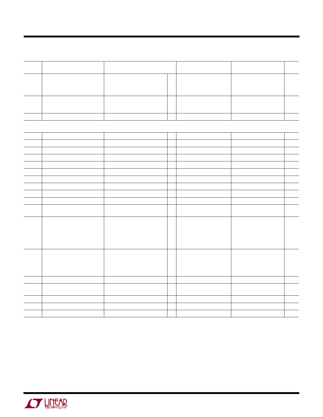
ELECTRICAL CHARACTERISTICS
SYMBOL PARAMETER CONDITIONS (Note 7) MIN TYP MAX MIN TYP MAX UNITS
G Gain Range G = 1 + (49.4k/RG) 1 10k 1 10k
Gain Error G = 1 0.008 0.02 0.015 0.03 %
G = 10 (Note 2) 0.010 0.08 0.020 0.10 %
G = 100 (Note 2) 0.025 0.08 0.030 0.10 %
G = 1000 (Note 2) 0.040 0.10 0.040 0.10 %
Gain Nonlinearity (Note 5) VO = ±10V, G = 1 1 6 1.5 10 ppm
= ±10V, G = 10 and 100 2 10 3 15 ppm
V
O
VO = ±10V, G = 1000 15 40 20 60 ppm
VO = ±10V, G = 1, RL = 600 5 12 6 15 ppm
VO = ±10V, G = 10 and 100, 6 15 7 20 ppm
= 600
R
L
= ±10V, G = 1000, 20 65 25 80 ppm
V
O
= 600
R
L
V
OST
V
OSI
V
OSO
I
OS
I
B
e
n
Total RTI Noise = √e
e
ni
e
no
2
Total Input Referred Offset Voltage V
Input Offset Voltage G = 1000, VS = ±5V to ±15V 15 40 20 60 µV
Output Offset Voltage G = 1, VS = ±5V to ±15V 40 200 50 300 µV
Input Offset Current 90 320 100 450 pA
Input Bias Current 50 350 80 500 pA
Input Noise Voltage, RTI 0.1Hz to 10Hz, G = 1 2.00 2.00 µV
2
+ (eno/G)
ni
Input Noise Voltage Density, RTI fO = 1kHz 7.5 12 7.5 12 nV/√Hz
Output Noise Voltage Density, RTI fO = 1kHz (Note 3) 67 90 67 90 nV/√Hz
2
= V
OST
OSI
0.1Hz to 10Hz, G = 10 0.50 0.50 µV
0.1Hz to 10Hz, G = 100 and 1000 0.28 0.28 µV
VS = ±15V, VCM = 0V, TA = 25°C, RL = 2k, unless otherwise noted.
LT1167C/LT1167I
+ V
OSO
LT1167AC/LT1167AI
/G
P-P
P-P
P-P
LT1167
ELECTRICAL CHARACTERISTICS
SYMBOL PARAMETER CONDITIONS (Note 7) MIN TYP MAX MIN TYP MAX UNITS
i
n
R
IN
C
IN(DIFF)
C
IN(CM)
V
CM
CMRR Common Mode 1k Source Imbalance,
PSRR Power Supply VS = ±2.3 to ±18V
I
S
V
OUT
I
OUT
BW Bandwidth G = 1 1000 1000 kHz
SR Slew Rate G = 1, V
R
REFIN
I
REFIN
V
REF
A
VREF
Input Noise Current fO = 0.1Hz to 10Hz 10 10 pA
Input Noise Current Density fO = 10Hz 124 124 fA/√Hz
Input Resistance VIN = ±10V 200 1000 200 1000 GΩ
Differential Input Capacitance fO = 100kHz 1.6 1.6 pF
Common Mode Input fO = 100kHz 1.6 1.6 pF
Capacitance
Input Voltage Range G = 1, Other Input Grounded
= ±2.3V to ±5V –VS + 1.9 +VS – 1.2 – VS + 1.9 +VS – 1.2 V
V
S
= ±5V to ±18V –VS + 1.9 +VS – 1.4 – VS + 1.9 +VS – 1.4 V
V
S
Rejection Ratio V
Rejection Ratio G = 1 105 120 100 120 dB
Supply Current VS = ±2.3V to ±18V 0.9 1.3 0.9 1.3 mA
Output Voltage Swing RL = 10k
Output Current 20 27 20 27 mA
Settling Time to 0.01% 10V Step
Reference Input Resistance 20 20 kΩ
Reference Input Current V
Reference Voltage Range –VS + 1.6 +VS – 1.6 – VS + 1.6 +VS – 1.6 V
Reference Gain to Output 1 ± 0.0001 1 ± 0.0001
= 0V to ±10V
CM
G = 1 90 95 85 95 dB
G = 10 106 115 100 115 dB
G = 100 120 125 110 125 dB
G = 1000 126 140 120 140 dB
G = 10 125 135 120 135 dB
G = 100 131 140 126 140 dB
G = 1000 135 150 130 150 dB
= ±2.3V to ±5V –VS + 1.1 +VS – 1.2 – VS + 1.1 +VS – 1.2 V
V
S
= ±5V to ±18V –VS + 1.2 +VS – 1.3 – VS + 1.2 +VS – 1.3 V
V
S
G = 10 800 800 kHz
G = 100 120 120 kHz
G = 1000 12 12 kHz
= ±10V 0.75 1.2 0.75 1.2 V/µs
OUT
G = 1 to 100 14 14 µs
G = 1000 130 130 µs
= 0V 50 50 µA
REF
VS = ±15V, VCM = 0V, TA = 25°C, RL = 2k, unless otherwise noted.
LT1167AC/LT1167AI LT1167C/LT1167I
P-P
3
LT1167
ELECTRICAL CHARACTERISTICS
VS = ±15V, VCM = 0V, 0°C ≤ TA ≤ 70°C, RL = 2k, unless otherwise noted.
LT1167AC LT1167C
SYMBOL PARAMETER CONDITIONS (Note 7) MIN TYP MAX MIN TYP MAX UNITS
Gain Error G = 1 ● 0.01 0.03 0.012 0.04 %
● 0.08 0.30 0.100 0.33 %
● 0.09 0.30 0.120 0.33 %
● 0.14 0.33 0.140 0.35 %
Gain Nonlinearity V
G = 10 (Note 2)
G = 100 (Note 2)
G = 1000 (Note 2)
= ±10V, G = 1 ● 1.5 10 2 15 ppm
OUT
V
= ±10V, G = 10 and 100 ● 3 15 4 20 ppm
OUT
= ±10V, G = 1000 ● 20 60 25 80 ppm
V
OUT
G/T Gain vs Temperature G < 1000 (Note 2) ● 20 50 20 50 ppm/°C
V
OST
Total Input Referred V
OST
= V
OSI
+ V
OSO
/G
Offset Voltage
V
V
V
V
V
V
I
OS
OSI
OSIH
OSO
OSOH
OSI
OSO
Input Offset Voltage VS = ±5V to ±15V ● 18 60 23 80 µV
Input Offset Voltage Hysteresis (Notes 3, 6) 3.0 3.0 µV
Output Offset Voltage VS = ±5V to ±15V ● 60 380 70 500 µV
Output Offset Voltage Hysteresis (Notes 3, 6) 30 30 µV
/T Input Offset Drift (RTI) (Note 3) ● 0.05 0.3 0.06 0.4 µV/°C
/T Output Offset Drift (Note 3) ● 0.7 3 0.8 4 µV/°C
Input Offset Current ● 100 400 120 550 pA
IOS/T Input Offset Current Drift ● 0.3 0.4 pA /°C
I
B
Input Bias Current ● 75 450 105 600 pA
IB/T Input Bias Current Drift ● 0.4 0.4 pA/°C
V
CM
Input Voltage Range G = 1, Other Input Grounded
VS = ±2.3V to ±5V ● –VS+2.1 + VS–1.3 –VS+2.1 + VS–1.3 V
= ±5V to ±18V ● –VS+2.1 + VS–1.4 –VS+2.1 + VS–1.4 V
V
S
CMRR Common Mode 1k Source Imbalance,
Rejection Ratio V
= 0V to ±10V
CM
G = 1
G = 10
G = 100
● 88 92 83 92 dB
● 100 110 97 110 dB
● 115 120 113 120 dB
G = 1000 ● 117 135 114 135 dB
PSRR Power Supply Rejection Ratio VS = ±2.3V to ±18V
G = 1
G = 10
G = 100
G = 1000
I
V
I
S
OUT
OUT
Supply Current VS = ±2.3V to ±18V ● 1.0 1.5 1.0 1.5 mA
Output Voltage Swing RL = 10k
= ±2.3V to ±5V ● –VS+1.4 + VS–1.3 –VS+1.4 +VS–1.3 V
V
S
= ±5V to ±18V ● –VS+1.6 + VS–1.5 –VS+1.6 + VS–1.5 V
V
S
Output Current ● 16 21 16 21 mA
SR Slew Rate G = 1, V
V
REF
REF Voltage Range (Note 3) ● –VS+1.6 + VS–1.6 –VS+1.6 + VS–1.6 V
= ±10V ● 0.65 1.1 0.65 1.1 V/µs
OUT
● 103 115 98 115 dB
● 123 130 118 130 dB
● 127 135 124 135 dB
● 129 145 126 145 dB
4
ELECTRICAL CHARACTERISTICS
VS = ±15V, VCM = 0V, –40°C ≤ TA ≤ 85°C, RL = 2k, unless otherwise noted. (Note 4)
LT1167
SYMBOL PARAMETER CONDITIONS (Note 7) MIN TYP MAX MIN TYP MAX UNITS
LT1167AI LT1167I
Gain Error G = 1 ● 0.014 0.04 0.015 0.05 %
G = 10 (Note 2) ● 0.130 0.40 0.140 0.42 %
G = 100 (Note 2)
● 0.140 0.40 0.150 0.42 %
G = 1000 (Note 2) ● 0.160 0.40 0.180 0.45 %
G
N
Gain Nonlinearity (Notes 2, 4) VO = ±10V, G = 1 ● 2 15 3 20 ppm
= ±10V, G = 10 and 100 ● 5 20 6 30 ppm
V
O
VO = ±10V, G = 1000 ● 26 70 30 100 ppm
G/T Gain vs Temperature G < 1000 (Note 2) ● 20 50 20 50 ppm/°C
V
V
V
V
V
V
V
I
OS
OST
OSI
OSIH
OSO
OSOH
OSI
OSO
Total Input Referred V
Offset Voltage
OST
= V
OSI
+ V
OSO
/G
Input Offset Voltage ● 20 75 25 100 µV
Input Offset Voltage Hysteresis (Notes 3, 6) 3.0 3.0 µV
Output Offset Voltage ● 180 500 200 600 µV
Output Offset Voltage Hysteresis (Notes 3, 6) 30 30 µV
/T Input Offset Drift (RTI) (Note 3) ● 0.05 0.3 0.06 0.4 µV/°C
/T Output Offset Drift (Note 3) ● 0.8 5 1 6 µV/°C
Input Offset Current ● 110 550 120 700 pA
IOS/T Input Offset Current Drift ● 0.3 0.3 pA/°C
I
B
Input Bias Current ● 180 600 220 800 pA
IB/T Input Bias Current Drift ● 0.5 0.6 pA/°C
V
CM
Input Voltage Range VS = ±2.3V to ±5V ● –VS + 2.1 +VS – 1.3 – VS + 2.1 +VS – 1.3 V
= ±5V to ±18V ● –VS + 2.1 +VS – 1.4 – VS + 2.1 +VS – 1.4 V
V
S
CMRR Common Mode Rejection Ratio 1k Source Imbalance,
VCM = 0V to ±10V
G = 1
G = 10
● 86 90 81 90 dB
● 98 105 95 105 dB
G = 100 ● 114 118 112 118 dB
G = 1000
● 116 133 112 133 dB
PSRR Power Supply Rejection Ratio VS = ±2.3V to ±18V
G = 1 ● 100 112 95 112 dB
G = 10
● 120 125 115 125 dB
G = 100 ● 125 132 120 132 dB
G = 1000
I
V
I
S
OUT
OUT
Supply Current ● 1.1 1.6 1.1 1.6 mA
Output Voltage Swing VS = ±2.3V to ±5V ● –VS + 1.4 +VS – 1.3 – VS + 1.4 +VS – 1.3 V
VS = ±5V to ±18V ● –VS + 1.6 +VS – 1.5 – VS + 1.6 +VS – 1.5 V
Output Current ● 15 20 15 20 mA
SR Slew Rate G = 1, V
V
REF
REF Voltage Range (Note 3) ● –VS + 1.6 +VS – 1.6 – VS + 1.6 +VS – 1.6 V
= ±10V ● 0.55 0.95 0.55 0.95 V/µs
OUT
● 128 140 125 140 dB
The ● denotes specifications that apply over the full specified
temperature range.
Note 1: Absolute Maximum Ratings are those values beyond which the life
of a device may be imparied.
Note 2: Does not include the effect of the external gain resistor R
.
G
Note 3: This parameter is not 100% tested.
Note 4: The LT1167AC/LT1167C are designed, characterized and expected
to meet the industrial temperature limits, but are not tested at –40°C and
85°C. I-grade parts are guaranteed.
Note 5: This parameter is measured in a high speed automatic tester that
does not measure the thermal effects with longer time constants. The
magnitude of these thermal effects are dependent on the package used,
heat sinking and air flow conditions.
Note 6: Hysteresis in offset voltage is created by package stress that
differs depending on whether the IC was previously at a higher or lower
temperature. Offset voltage hysteresis is always measured at 25°C, but
the IC is cycled to 85°C I-grade (or 70°C C-grade) or –40°C I-grade
(0°C C-grade) before successive measurement. 60% of the parts will
pass the typical limit on the data sheet.
Note 7: Typical parameters are defined as the 60% of the yield parameter
distribution.
5
LT1167
TEMPERATURE (°C)
–50
GAIN ERROR (%)
–0.20
–0.10
–0.05
0
50
0.20
1167 G06
–0.15
0
–25
75
G = 1
25 100
0.05
0.10
0.15
VS = ±15V
V
OUT
= ±10V
R
L
= 2k
*DOES NOT INCLUDE
TEMPERATURE EFFECTS
OF R
G
G = 10*
G = 1000*
G = 100*
UW
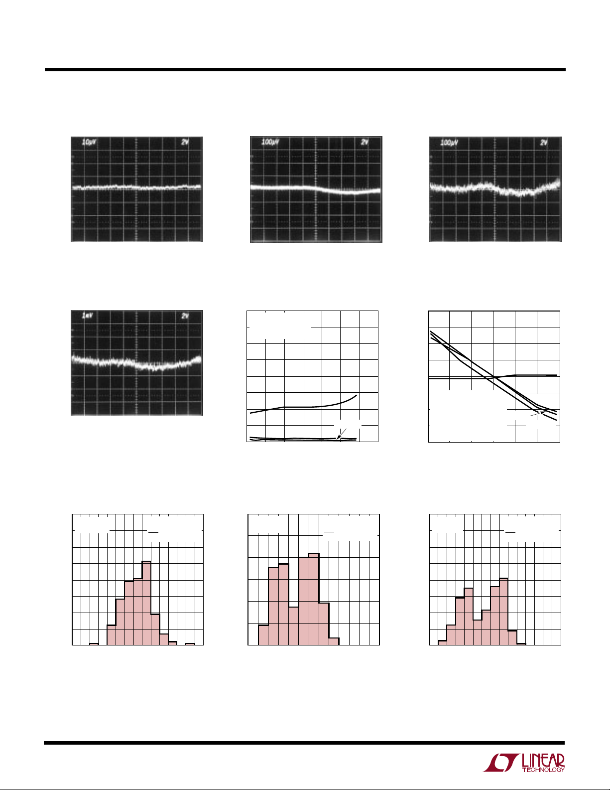
TYPICAL PERFOR A CE CHARACTERISTICS
Gain Nonlinearity, G = 1
NONLINEARITY (1ppm/DIV)
G = 1
R
V
OUTPUT VOLTAGE (2V/DIV)
= 2k
L
= ±10V
OUT
Gain Nonlinearity, G = 1000
NONLINEARITY (100ppm/DIV)
G = 1000
RL = 2k
V
OUTPUT VOLTAGE (2V/DIV)
= ±10V
OUT
1167 G01
1167 G04
Gain Nonlinearity, G = 10
NONLINEARITY (10ppm/DIV)
G = 10
RL = 2k
V
OUTPUT VOLTAGE (2V/DIV)
= ±10V
OUT
Gain Nonlinearity vs Temperature
80
VS = ±15V
= –10V TO 10V
V
OUT
70
= 2k
R
L
60
50
40
30
NONLINEARITY (ppm)
20
10
0
–25 0 50
–50
G = 1000
G = 100
25
TEMPERATURE (°C)
G = 1, 10
75 100 150
1167 G02
1167 G05
Gain Nonlinearity, G = 100
NONLINEARITY (10ppm/DIV)
G = 100
RL = 2k
V
OUTPUT VOLTAGE (2V/DIV)
= ±10V
OUT
Gain Error vs Temperature
1167 G03
6
Distribution of Input
Offset Voltage, TA = –40°C
40
VS = ±15V
G = 1000
35
30
25
20
15
PERCENT OF UNITS (%)
10
5
0
–80
–60 –40 –20 20 40 60
INPUT OFFSET VOLTAGE (µV)
137 N8 (2 LOTS)
165 S8 (3 LOTS)
302 TOTAL PARTS
0
1167 G40
Distribution of Input
Offset Voltage, TA = 25°C
30
VS = ±15V
G = 1000
25
20
15
10
PERCENT OF UNITS (%)
5
0
–60 – 40 –20 0 20 40 60
INPUT OFFSET VOLTAGE (µV)
137 N8 (2 LOTS)
165 S8 (3 LOTS)
302 TOTAL PARTS
1167 G41
Distribution of Input
Offset Voltage, TA = 85°C
40
VS = ±15V
G = 1000
35
30
25
20
15
PERCENT OF UNITS (%)
10
5
0
–80
–60 –40 –20 20 40 60
INPUT OFFSET VOLTAGE (µV)
137 N8 (2 LOTS)
165 S8 (3 LOTS)
302 TOTAL PARTS
0
1167 G42
 Loading...