

Linear Technology LT1125, LT1124 Datasheet
FEATURES
■
100% Tested Low Voltage Noise: 2.7nV/√Hz Typ
4.2nV/√Hz Max
■
Slew Rate: 4.5V/µs Typ
■
Gain Bandwidth Product: 12.5MHz Typ
■
Offset Voltage, Prime Grade: 70µV Max
Low Grade: 100µV Max
■
High Voltage Gain: 5 Million Min
■
Supply Current Per Amplifier: 2.75mA Max
■
Common Mode Rejection: 112dB Min
■
Power Supply Rejection: 116dB Min
■
Available in 8-Pin SO Package
U
APPLICATIO S
■
Two and Three Op Amp Instrumentation Amplifiers
■
Low Noise Signal Processing
■
Active Filters
■
Microvolt Accuracy Threshold Detection
■
Strain Gauge Amplifiers
■
Direct Coupled Audio Gain Stages
■
Tape Head Preamplifiers
■
Infrared Detectors
, LTC and LT are registered trademarks of Linear Technology Corporation.
Protected by U.S. patents 4,775,884 and 4,837,496.
LT1124/LT1125
Dual/Quad Low Noise,
High Speed Precision Op Amps
U
DESCRIPTIO
The LT®1124 dual and LT1125 quad are high performance
op amps that offer higher gain, slew rate and bandwidth
than the industry standard OP-27 and competing OP-270/
OP-470 op amps. In addition, the LT1124/LT1125 have
lower IB and I
than the OP-270/OP-470.
In the design, processing and testing of the device, particular attention has been paid to the optimization of the
entire distribution of several key parameters. Slew rate,
gain bandwidth and 1kHz noise are 100% tested for each
individual amplifier. Consequently, the specifications of
even the lowest cost grades (the LT1124C and the
LT1125C) have been spectacularly improved compared
to equivalent grades of competing amplifiers.
Power consumption of the LT1124 is one half of two
OP-27s. Low power and high performance in an 8-pin SO
package make the LT1124 a first choice for surface mounted
systems and where board space is restricted.
For a decompensated version of these devices, with three
times higher slew rate and bandwidth, please see the
LT1126/LT1127 data sheet.
than the OP-27; lower VOS and noise
OS
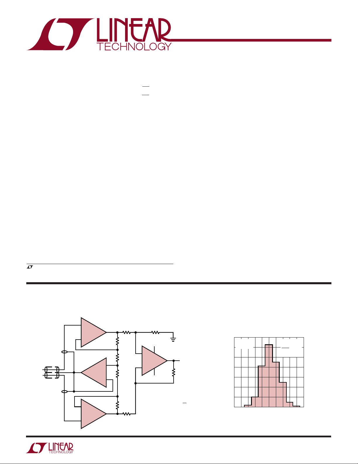
TYPICAL APPLICATIO
Instrumentation Amplifier with Shield Driver
3
INPUT
+
1/4
LT1125
2
–
GUARD
+
8
–
GUARD
13
–
1/4
LT1125
12
+
1/4
LT1125
1
10
+
9
–
14
U
R
F
3.4k
R
G
100Ω
R
G
100Ω
R
F
3.4k
1k
30k1k
15V
5
4
+
1/4
LT1125
6
–
11
–15V
GAIN
POWER BW
SMALL-SIGNAL BW
NOISE
V
7
OUTPUT
30k
= 30 (1 + RF/RG) ≈ 1000
= 170kHz
= 400kHz
= 3.8µV/ Hz AT OUTPUT
√
= 35µV
OS
1124/25 TA01
Input Offset Voltage Distribution
(All Packages, LT1124 and LT1125)
DUALS
VS = ±15V
T
= 25°C
A
30
20
PERCENT OF UNITS
10
0
–60 –20
–100
INPUT OFFSET VOLTAGE (µV)
758
QUADS
200
2316 UNITS
TESTED
60
1124/25 TA02
10020
1
LT1124/LT1125
1
2
3
4
8
7
6
5
TOP VIEW
OUT A
–IN A
+IN A
V
–
V
+
OUT B
–IN B
+IN B
N8 PACKAGE
8-LEAD PDIP
J8 PACKAGE
8-LEAD CERDIP
A
B
1
2
3
4
5
6
7
TOP VIEW
N PACKAGE
14-LEAD PDIP
J PACKAGE
14-LEAD CERDIP
14
13
12
11
10
9
8
OUT A
–IN A
+IN A
V
+
+IN B
–IN B
OUT B
OUT D
–IN D
+IN D
V
–
+IN C
–IN C
OUT C
B
A
C
D
A
W
O
LUTEXI TIS
S
A
WUW
U
(Note 1)
ARB
G
Supply Voltage ..................................................... ±22V
Input Voltages ......................... Equal to Supply Voltage
Output Short-Circuit Duration......................... Indefinite
Differential Input Current (Note 6) ..................... ±25mA
Lead Temperature (Soldering, 10 sec)................. 300°C
Storage Temperature Range ................ –65°C to 150°C
/
PACKAGE
+IN A
–
V
+IN B
–IN B
T
NOTE: THIS PIN CONFIGURATION DIFFERS FROM THE
8-PIN PDIP CONFIGURATION. INSTEAD, IT FOLLOWS
THE INDUSTRY STANDARD LT1013DS8 SO PACKAGE
PIN LOCATIONS
O
RDER I FOR ATIO
TOP VIEW
1
2
A
3
B
4
S8 PACKAGE
8-LEAD PLASTIC SO
= 140°C, θJA = 190°C
JMAX
8
–IN A
OUT A
7
+
V
6
OUT B
5
WU
ORDER PART
NUMBER
LT1124CS8
LT1124AIS8
LT1124IS8
S8 PART MARKING
1124
1124AI
1124I
U
Operating Temperature Range
LT1124AC/LT1124C
LT1125AC/LT1125C (Note 10) .......... – 40°C to 85°C
LT1124AI/LT1124I ............................ –40°C to 85°C
LT1124AM/LT1124M
LT1125AM/LT1125M ...................... –55°C to 125°C
ORDER PART
NUMBER
LT1124CJ8
LT1124ACN8
LT1124CN8
LT1124AMJ8
LT1124MJ8
T
= 160°C, θJA = 100°C (J8)
JMAX
= 140°C, θJA = 130°C (N8)
T
JMAX
TOP VIEW
1
OUT A
2
–IN A
+IN A
+
V
+IN B
–IN B
OUT B
NC
LECTRICAL C CHARA TERIST
E
A
3
4
5
B
6
7
8
SW PACKAGE
16-LEAD PLASTIC (WIDE) SO
T
= 140°C, θJA = 130°C
JMAX
16
OUT D
15
D
C
–IN D
14
+IN D
–
13
V
12
+IN C
11
–IN C
10
OUT C
9
NC
LT1125CS
ICS
TA = 25°C, VS = ±15V, unless otherwise noted.
T
= 160°C, θJA = 80°C (J)
JMAX
T
= 140°C, θJA = 110°C (N)
JMAX
LT1125CJ
LT1125ACN
LT1125CN
LT1125AMJ
LT1125MJ
LT1124AC/AI/AM LT1124/C/I/M
LT1125AC/AM LT1125/C/M
SYMBOL PARAMETER CONDITIONS (Note 2) MIN TYP MAX MIN TYP MAX UNITS
V
OS
∆V
OS
∆Time Voltage Stability
I
OS
2
Input Offset Voltage LT1124 20 70 25 100 µV
LT1125 25 90 30 140 µV
Long Term Input Offset 0.3 0.3 µV/Mo
Input Offset Current LT1124 5 15 6 20 nA
LT1125 6 20 7 30 nA
LT1124/LT1125
LECTRICAL C CHARA TERIST
E
SYMBOL PARAMETER CONDITIONS (Note 2) MIN TYP MAX MIN TYP MAX UNITS
I
B
e
n
i
n
V
CM
CMRR Common Mode Rejection Ratio VCM = ±12V 112 126 106 124 dB
PSRR Power Supply Rejection Ratio VS = ±4V to ±18V 116 126 110 124 dB
A
VOL
V
OUT
SR Slew Rate RL ≥ 2k (Notes 3, 7) 3 4.5 2.7 4.5 V/µs
GBW Gain Bandwidth Product fO = 100kHz (Note 3) 9 12.5 8 12.5 MHz
Z
O
I
S
Input Bias Current ±7 ±20 ±8 ±30 nA
Input Noise Voltage 0.1Hz to 10Hz (Notes 8, 9) 70 200 70 nV
Input Noise Voltage Density fO = 10Hz (Note 4) 3.0 5.5 3.0 5.5 nV/√Hz
f
Input Noise Current Density fO = 10Hz 1.3 1.3 pA/√Hz
f
Input Voltage Range ±12 ±12.8 ±12 ±12.8 V
Large-Signal Voltage Gain RL ≥ 10k, V
R
Maximum Output Voltage Swing RL ≥ 2k ±13 ±13.8 ±12.5 ±13.8 V
Open-Loop Output Resistance V
Supply Current per Amplifier 2.3 2.75 2.3 2.75 mA
Channel Separation f ≤ 10Hz (Note 9) 134 150 130 150 dB
V
ICS
= 1000Hz (Note 3) 2.7 4.2 2.7 4.2 nV/√Hz
O
= 1000Hz 0.3 0.3 pA/√Hz
O
≥ 2k, V
L
= 0, I
OUT
= ±10V, RL = 2k
OUT
TA = 25°C, VS = ±15V, unless otherwise noted.
LT1124AC/AI/AM LT1124C/I/M
LT1125AC/AM LT1125C/M
= ±10V 5 17 3.0 15 V/µV
OUT
= ±10V 2 4 1.5 3 V/µV
OUT
= 0 75 75 Ω
OUT
P-P
The ● denotes the specifications which apply over the –55°C ≤ TA ≤ 125°C temperature range, VS = ±15V, unless otherwise noted.
LT1124AM LT1124M
LT1125AM LT1125M
SYMBOL PARAMETER CONDITIONS (Note 2) MIN TYP MAX MIN TYP MAX UNITS
V
OS
∆V
OS
∆Temp Voltage Drift
I
OS
I
B
V
CM
CMRR Common Mode Rejection Ratio VCM = ±11.3V ● 106 122 100 120 dB
PSRR Power Supply Rejection Ratio VS = ±4V to ±18V ● 110 122 104 120 dB
A
VOL
V
OUT
SR Slew Rate RL ≥ 2k (Notes 3, 7) ● 2.3 3.8 2 3.8 V/µs
I
S
Input Offset Voltage LT1124 ● 50 170 60 250 µV
LT1125
Average Input Offset (Note 5) ● 0.3 1.0 0.4 1.5 µV/°C
Input Offset Current LT1124 ● 18 45 20 60 nA
LT1125
Input Bias Current ● ±18 ±55 ±20 ±70 nA
Input Voltage Range ● ±11.3 ±12 ±11.3 ±12 V
Large-Signal Voltage Gain RL ≥ 10k, V
≥ 2k, V
R
L
Maximum Output Voltage Swing RL ≥ 2k ● ±12.5 ±13.6 ±12 ±13.6 V
Supply Current per Amplifier ● 2.5 3.25 2.5 3.25 mA
= ±10V ● 3 10 2.0 10 V/µV
OUT
= ±10V ● 1 3 0.7 2 V/µV
OUT
● 55 190 70 290 µV
● 18 55 20 70 nA
3
LT1124/LT1125
LECTRICAL C CHARA TERIST
E
ICS
The ● denotes the specifications which apply over the 0°C ≤ TA ≤ 70°C
temperature range, VS = ±15V, unless otherwise noted.
LT1124AC LT1124C
SYMBOL PARAMETER CONDITIONS (Note 2) MIN TYP MAX MIN TYP MAX UNITS
V
OS
∆V
OS
∆Temp Voltage Drift
I
OS
I
B
V
CM
CMRR Common Mode Rejection Ratio VCM = ±11.5V ● 109 125 102 122 dB
PSRR Power Supply Rejection Ratio VS = ±4V to ±18V ● 112 125 107 122 dB
A
VOL
V
OUT
SR Slew Rate RL ≥ 2k (Notes 3, 7) ● 2.6 4 2.4 4 V/µs
I
S
Input Offset Voltage LT1124 ● 35 120 45 170 µV
LT1125 ● 40 140 50 210 µV
Average Input Offset (Note 5) ● 0.3 1 0.4 1.5 µV/°C
Input Offset Current LT1124 ● 625 735 nA
LT1125 ● 735 845 nA
Input Bias Current ● ±8 ±35 ±9 ±45 nA
Input Voltage Range ● ±11.5 ±12.4 ±11.5 ±12.4 V
Large-Signal Voltage Gain RL ≥ 10k, V
Maximum Output Voltage Swing RL ≥ 2k ● ±12.5 ±13.7 ±12 ±13.7 V
Supply Current per Amplifier ● 2.4 3 2.4 3 mA
≥ 2k, V
R
L
= ±10V ● 4.0 15 2.5 14 V/µV
OUT
= ±10V ● 1.5 3.5 1.0 2.5 V/µV
OUT
LT1125AC LT1125C
The ● denotes the specifications which apply over the –40°C ≤ TA ≤ 85°C temperature range, VS = ±15V,
unless otherwise noted. (Note 10)
LT1124AC/AI LT1124C/I
SYMBOL PARAMETER CONDITIONS (Note 2) MIN TYP MAX MIN TYP MAX UNITS
V
OS
∆V
OS
∆Temp Voltage Drift
I
OS
I
B
V
CM
CMRR Common Mode Rejection Ratio VCM = ±11.4V ● 107 124 101 121 dB
PSRR Power Supply Rejection Ratio VS = ±4V to ±18V ● 111 124 106 121 dB
A
VOL
V
OUT
SR Slew Rate RL ≥ 2k (Notes 3, 7) ● 2.4 3.9 2.1 3.9 V/µs
I
S
Note 1: Absolute Maximum Ratings are those values beyond which the life
of a device may be impaired.
Note 2: Typical parameters are defined as the 60% yield of parameter
distributions of individual amplifiers; i.e., out of 100 LT1125s (or 100
LT1124s) typically 240 op amps (or 120) will be better than the indicated
specification.
Note 3: This parameter is 100% tested for each individual amplifier.
Note 4: This parameter is sample tested only.
Note 5: This parameter is not 100% tested.
Note 6: The inputs are protected by back-to-back diodes. Current limiting
resistors are not used in order to achieve low noise. If differential input
voltage exceeds ±1.4V, the input current should be limited to 25mA.
Input Offset Voltage LT1124 ● 40 140 50 200 µV
LT1125 ● 45 160 55 240 µV
Average Input Offset (Note 5) ● 0.3 1 0.4 1.5 µV/°C
Input Offset Current LT1124 ● 15 40 17 55 nA
Input Bias Current ● ±15 ±50 ±17 ±65 nA
Input Voltage Range ● ±11.4 ±12.2 ±11.4 ±12.2 V
Large-Signal Voltage Gain RL ≥ 10k, V
Maximum Output Voltage Swing RL ≥ 2k ● ±12.5 ±13.6 ±12 ±13.6 V
Supply Current per Amplifier ● 2.4 3.25 2.4 3.25 mA
LT1125
≥ 2k, V
R
L
= ±10V ● 3.5 12 2.2 12 V/µV
OUT
= ±10V ● 1.2 3.2 0.8 2.3 V/µV
OUT
● 15 50 17 65 nA
Note 7: Slew rate is measured in AV = –1; input signal is ±7.5V, output
measured at ±2.5V.
Note 8: 0.1Hz to 10Hz noise can be inferred from the 10Hz noise voltage
density test. See the test circuit and frequency response curve for 0.1Hz to
10Hz tester in the Applications Information section of the LT1007 or
LT1028 data sheets.
Note 9: This parameter is guaranteed but not tested.
Note 10: The LT1124C/LT1125C and LT1124AC/LT1125AC are guaranteed
to meet specified performance from 0°C to 70°C and are designed,
characterized and expected to meet these extended temperature limits, but
are not tested at –40°C and 85°C. The LT1124AI and LT1124I are
guaranteed to meet the extended temperature limits.
LT1125AC LT1125C
4
LT1124/LT1125
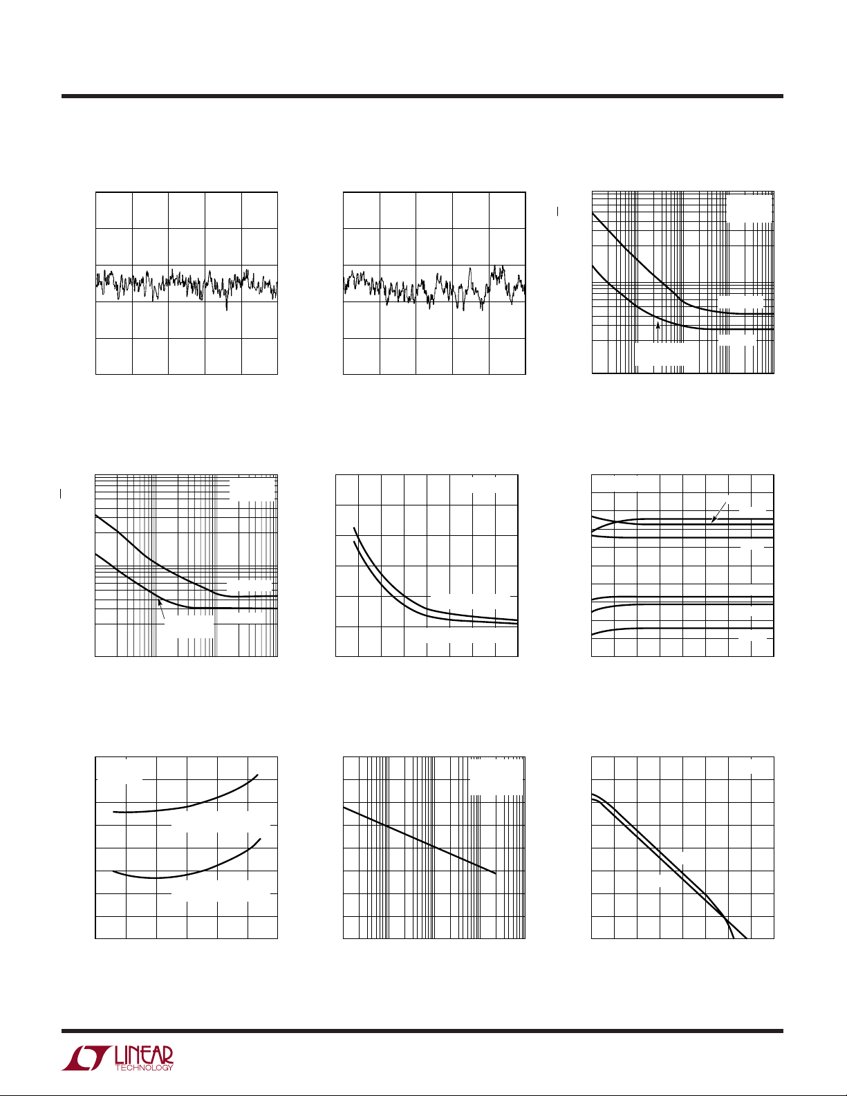
FREQUENCY (Hz)
1
0
POWER SUPPLY REJECTION RATIO (dB)
20
40
120
140
160
10
2
10
8
1124/25 G09
10 10310410510610
7
60
100
80
–PSRR
+PSRR
TA = 25°C
UW
LPER
F
O
R
ATYPICA
0.1Hz to 10Hz Voltage Noise 0.01Hz to 1Hz Voltage Noise Voltage Noise vs Frequency
VOLTAGE NOISE (40nV/DIV)
0
26810
4
TIME (SECONDS)
1124/25 G01
Current Noise vs Frequency vs Temperature vs Time
10.0
√
3.0
1.0
0.3
RMS CURRENT NOISE DENSITY (pA/ Hz)
0.1
10 1k 10k
1/f CORNER
100Hz
100
FREQUENCY (Hz)
VS = ±15V
= 25°C
T
A
MAXIMUM
TYPICAL
1124 G04
CCHARA TERIST
E
C
VOLTAGE NOISE (40nV/DIV)
0
20 60 80 100
Input Bias or Offset Current Output Short-Circuit Current
30
20
10
INPUT BIAS OR OFFSET CURRENT (nA)
0
–75
–25 0 50 100
–50 25 75 125
TEMPERATURE (°C)
40
TIME (SECONDS)
LT1124M/LT1125M
LT1124AM/LT1125AM
ICS
VS = ±15V
1124/25 G02
1124/25 G05
100
√
30
10
3
VS = ±15V
1/f CORNER
2.3Hz
1.0
FREQUENCY (Hz)
1
234
RMS VOLTAGE NOISE DENSITY (nV/ Hz)
1
0.1 10 100 1000
50
40
30
20
10
0
–10
–20
–30
SHORT-CIRCUIT CURRENT (mA)
SINKING SOURCING
–40
–50
0
TIME FROM OUTPUT SHORT TO GND (MINUTES)
VS = ±15V
= 25°C
T
A
MAXIMUM
TYPICAL
1124/25 G03
25°C
–55°C
125°C
125°C
25°C
–55°C
LT1124 G06
Input Bias Current Over the Common Mode Rejection Ratio Power Supply Rejection Ratio
Common Mode Range vs Frequency vs Frequency
20
VS = ±15V
= 25°C
T
A
15
10
5
0
–5
–10
INPUT BIAS CURRENT (nA)
–15
–20
–10 5 15
–15
COMMON MODE INPUT VOLTAGE (V)
DEVICE WITH POSITIVE
INPUT CURRENT
DEVICE WITH NEGATIVE
INPUT CURRENT
–5 10
0
1124/25 G07
160
140
120
100
80
60
40
20
COMMON MODE REJECTION RATIO (dB)
0
1k 100k 1M 10M
10k
FREQUENCY (Hz)
TA = 25°C
V
S
V
CM
= ±15V
= ±10V
1124/25 G08
5
 Loading...