

FEATURES
■
Extremely Low Dropout
■
Low Cost
■
Fixed 5V Output, Trimmed to ±1%
■
700µA Quiescent Current
■
1mV Line Regulation
■
5mV Load Regulation
■
Thermal Limit
■
4A Output Current Guaranteed
■
Available in a 3-Pin TO-92 Package
LT1123
Low Dropout
Regulator Driver
U
DESCRIPTIO
The LT®1123 is a 3-pin bipolar device designed to be used
in conjunction with a discrete PNP power transistor to
form an inexpensive low dropout regulator. The LT1123
consists of a trimmed bandgap reference, error amplifier,
and a driver circuit capable of sinking up to 125mA from
the base of the external PNP pass transistor. The LT1123
is designed to provide a fixed output voltage of 5V.
The drive pin of the device can pull down to 2V at 125mA
(1.4V at 10mA). This allows a resistor to be used to reduce
the base drive available to the PNP and minimize the
power dissipation in the LT1123. The drive current of the
LT1123 is folded back as the feedback pin approaches
ground to further limit the available drive current under
short-circuit conditions.
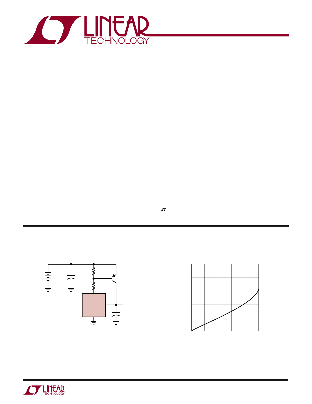
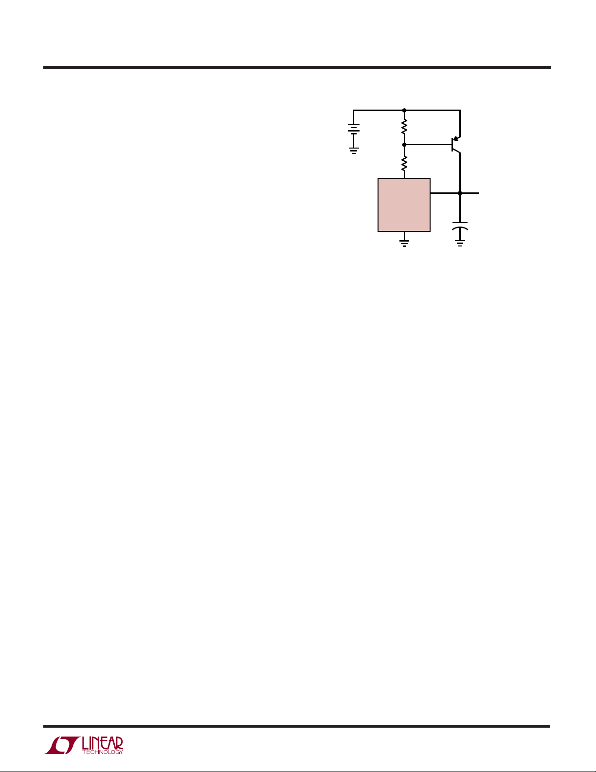
TYPICAL APPLICATIO
5V Low Dropout Regulator Dropout Voltage
SEALED
LEAD ACID
5.4 TO 7.2V
*REQUIRED IF DEVICE IS
MORE THAN 6" FROM MAIN
FILTER CAPACITOR
†
REQUIRED FOR STABILITY
(LARGER VALUES INCREASE
STABILITY)
+
10µF*
DRIVE
LT1123
GND
620Ω
20Ω
FB
U
MOTOROLA
MJE1123
+
LT1123 TA01
OUTPUT = 5V/4A
†
10µF
Total quiescent current for the LT1123 is only 700µA. The
device is available in a low cost TO-92 package.
, LTC and LT are registered trademarks of Linear Technology Corporation.
All other trademarks are the property of their respective owners.
0.5
0.4
0.3
0.2
DROPOUT VOLTAGE (V)
0.1
0
1
0
OUTPUT CURRENT (A)
3
4
2
5
LT1123 TA02
1123fb
1
LT1123
WWWU
ABSOLUTE AXI U RATI GS
(Note 1)
Drive Pin Voltage (V
Feedback Pin Voltage (V
to Ground) ..................... 30V
DRIVE
to Ground) .................... 30V
FB
Storage Temperature Range ................. –65°C to 150°C
Lead Temperature (Soldering, 10 sec)................. 300°C
Operating Junction Temperature Range ... 0°C to 125°C
UU
W
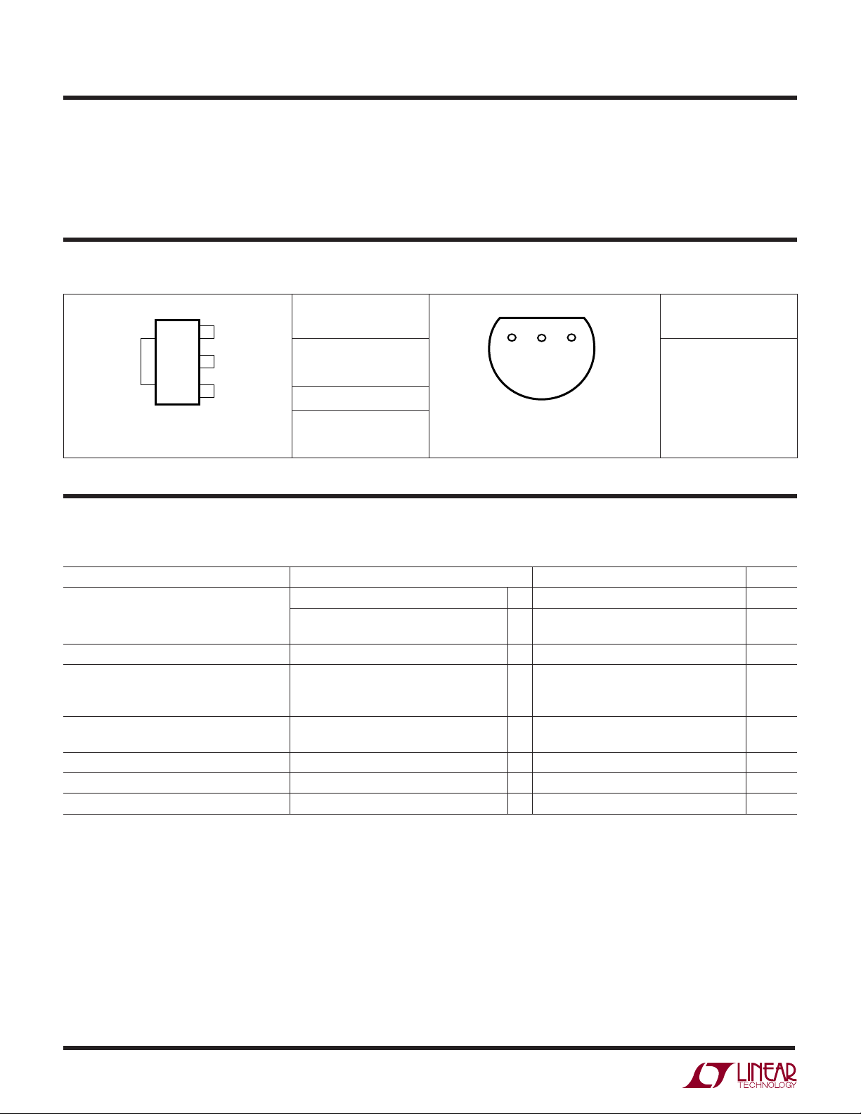
PACKAGE/ORDER I FOR ATIO
FRONT VIEW
3
FB
TAB IS
GND
ST PACKAGE
3-LEAD PLASTIC SOT-223
θJA AT TAB ≈ 20°C/W
Consult LTC Marketing for parts specified with wider operating temperature ranges.
2
GND
1
DRIVE
ORDER PART
NUMBER
LT1123CST
ST PART MARKING
1123
BOTTOM VIEW
DRIVE FB GND
Z PACKAGE
3-LEAD TO-92 PLASTIC
= 125°C, θJA = 220°C/W
T
JMAX
ORDER PART
NUMBER
LT1123CZ
ELECTRICAL CHARACTERISTICS
The ● denotes the specifications which apply over the full operating temperature range, otherwise specifications are at TA = 25°C.
PARAMETER CONDITIONS MIN TYP MAX UNITS
Feedback Voltage I
Feedback Pin Bias Current VFB = 5.00V, 2V ≤ V
Drive Current VFB = 5.20V, 2V ≤ V
Drive Pin Saturation Voltage I
Line Regulation 5V < V
Load Regulation ∆I
Temperature Coefficient of V
OUT
= 10mA, TJ = 25°C 4.90 5.00 5.10 V
DRIVE
5mA ≤ I
3V ≤ V
= 4.80V, V
V
FB
V
= 0.5V, V
FB
DRIVE
I
DRIVE
DRIVE
≤ 100mA
DRIVE
≤ 20V ● 4.80 5.00 5.20 V
DRIVE
≤ 15V ● 300 500 µA
DRIVE
≤ 15V ● 0.45 1.0 mA
DRIVE
= 3V ● 125 170
DRIVE
= 3V, 0°C ≤ TJ ≤ 100°C 25 100 150
DRIVE
= 10mA, VFB = 4.5V 1.4 V
= 125mA, VFB = 4.5V 2.0
< 20V ● 1.0 ±20 mV
DRIVE
= 10 to 100mA ● –5 –50 mV
0.2 mV/°C
Note 1: Absolute Maximum Ratings are those values beyond which the life
of the device may be impaired.
2
1123fb
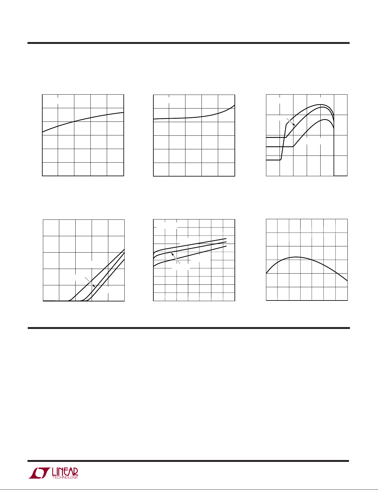
TEMPERATURE (°C)
–50
OUTPUT VOLTAGE (V)
5.01
5.02
5.03
25 75
LT1123 G06
5.00
4.99
–25 0
50 100 125
4.98
4.97
LPER
FEEDBACK PIN VOLTAGE (V)
0
0
DRIVE CURRENT (mA)
50
100
150
1234
LT1123 G03
56
200
TJ = 125°C
TJ = –50°C
TJ = 25°C
V
DRIVE
= 3V
LT1123
UW
R
F
O
ATYPICA
CCHARA TERIST
E
C
ICS
Feedback Pin Bias Current
vs Temperature
400
VFB = 5V
300
200
FEEDBACK PIN BIAS CURRENT (µA)
100
0
25 50 75 100
TEMPERATURE (°C)
Feedback Pin Bias Current
vs Feedback Pin Voltage
500
400
300
200
TJ = 25°C
100
FEEDBACK PIN BIAS CURRENT (µA)
TJ = 125°C
LT1123 G01
TJ = 0°C
125
Minimum Drive Pin Current
vs Temperature
600
V
= 3V
DRIVE
500
400
300
200
100
MINIMUM DRIVE PIN CURRENT (µA)
0
0
25 50 75 100
TEMPERATURE (°C)
Drive Pin Saturation Voltage
vs Drive Current
2.5
VFB = 4.5V
2.0
1.5
1.0
DRIVE PIN VOLTAGE (V)
0.5
TJ = 0°C
TJ = 125°C
TJ = 25°C
Drive Current
vs Feedback Pin Voltage
125
LT1123 G02
Output Voltage vs Temperature
0
PI FU CTIO S
Drive Pin: The drive pin serves two functions. It provides
current to the LT1123 for its internal circuitry including
start-up, bias, current limit, thermal limit and a portion of
the base drive current for the output Darlington. The sum
total of these currents (450µA typical) is equal to the
minimum drive current. This current is listed in the specifications as Drive Current with VFB = 5.2V. This is the
minimum current required by the drive pin of the LT1123.
The second function of the drive pin is to sink the base
drive current of the external PNP pass transistor. The
available drive current is specified for two conditions.
1
0
FEEDBACK PIN VOLTAGE (V)
U
3
2
4
UU
LT1123 G04
0
5
0
40
20
DRIVE CURRENT (mA)
80
60
100
120
LT1123 G05
140
Drive current with VFB = 4.80V gives the range of current
available under nominal operating conditions, when the
device is regulating. Drive current with VFB = 0.5V gives the
range of drive current available with the feedback pin
pulled low as it would be during start-up or during a shortcircuit fault. The drive current available when the feedback
pin is pulled low is less than the drive current available
when the device is regulating (VFB = 5V). This can be seen
in the curve of Drive Current vs VFB Voltage in the Typical
Performance Characteristics curves. This can provide
some foldback in the current limit of the regulator circuit.
1123fb
3
LT1123
U
UU
PI FU CTIO S
All internal circuitry connected to the drive pin is designed
to operate at the saturation voltage of the Darlington
output driver (1.4 to 2V). This allows a resistor to be
inserted between the base of the external PNP device and
the drive pin. This resistor is used to limit the base drive to
the external PNP below the value set internally by the
LT1123, and also to help limit power dissipation in the
LT1123. The operating voltage range of this pin is from
0V to 30V. Pulling this pin below ground by more than one
V
will forward bias the substrate diode of the device.
BE
This condition can only occur if the power supply leads are
W
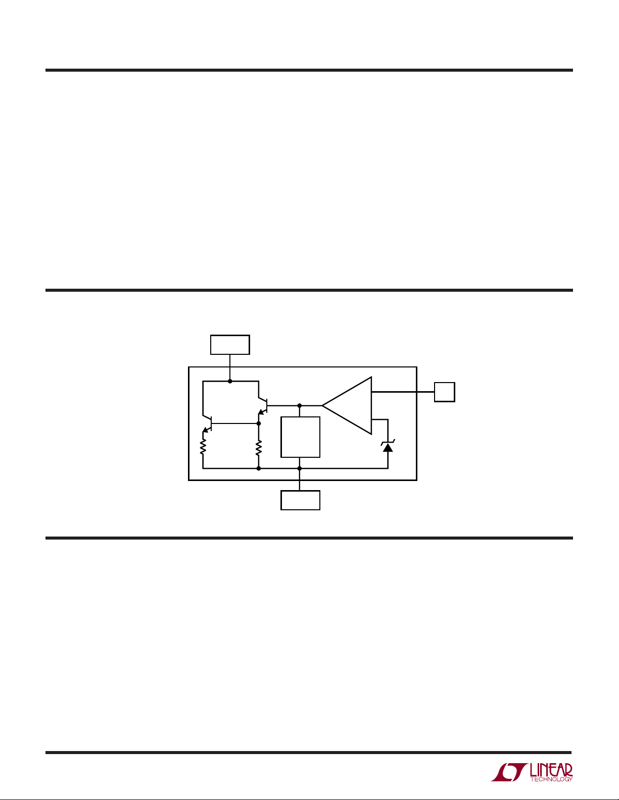
SI PLIFIEDWBLOCK DIAGRA
DRIVE
reversed and will not damage the device if the current is
limited to less than 200mA.
Feedback Pin (V
functions. It provides a path for the bias current of the
reference and error amplifier and contributes a portion of
the drive current for the Darlington output driver. The sum
total of these currents is the Feedback Pin Bias Current
(300µA typical). The second function of this pin is to
provide the voltage feedback to the error amplifier.
): The feedback pin also serves two
FB
CURRENT
LIMIT
THERMAL
LIMIT
GROUND
U
U
U
FU CTIO AL DESCRIPTIO
The LT1123 is a 3-pin device designed to be used in
conjunction with a discrete PNP transistor to form an
inexpensive ultralow dropout regulator. The device incorporates a trimmed 5V bandgap reference, error amplifier,
a current-limited Darlington driver and an internal thermal
limit circuit. The internal circuitry connected to the drive
pin is designed to function at the saturation voltage of the
Darlington driver. This allows a resistor to be inserted in
–
+
5V
LT1123 SBD01
series with the drive pin. This resistor is used to limit the
base drive to the PNP and also to limit the power dissipation in the LT1123. The value of this resistor will be defined
by the operating requirements of the regulator circuit. The
LT1123 is designed to sink a minimum of 125mA of base
current. This is sufficient base drive to form a regulator
circuit which can supply output currents up to 4A at a
dropout voltage of less than 0.75V.
FB
4
1123fb
WUUU
APPLICATIO S I FOR ATIO
LT1123
The LT1123 is designed to be used in conjunction with an
external PNP transistor. The overall specifications of a
regulator circuit using the LT1123 and an external PNP will
be heavily dependent on the specifications of the external
PNP. While there are a wide variety of PNP transistors
available that can be used with the LT1123, the specifications given in typical transistor data sheets are of little use
in determining overall circuit performance.
Linear Technology has solved this problem by cooperating
with Motorola to design and specify the MJE1123. This
transistor is specifically designed to work with the LT1123
as the pass element in a low dropout regulator. The
specifications of the MJE1123 reflect the capability of the
LT1123. For example, the dropout voltage of the MJE1123
is specified up to 4A collector current with base drive
currents that the LT1123 is capable of generating (20mA
to 120mA). Output currents up to 4A with dropout voltages
less than 0.75V can be guaranteed.
The following sections describe how specifications can be
determined for the basic regulator. The charts and graphs
are based on the combined characteristics of the LT1123
and the MJE1123. Formulas are included that will enable
the user to substitute other transistors that have been
characterized. A chart is supplied that lists suggested
resistor values for the most popular range of input voltages and output current.
Basic Regulator Circuit
The basic regulator circuit is shown in Figure 1. The
LT1123 senses the voltage at its feedback pin and drives
the base of the PNP (MJE1123) in order to maintain the
output at 5V. The drive pin of the LT1123 can only sink
current; RB is required to provide pull up on the base of the
PNP. RB must be sized so that the voltage drop caused by
the minimum drive pin current is less than the emitter/
base voltage of the external PNP at light loads. The
recommended value for RB is 620Ω. For circuits that are
required to run at junction temperatures in excess of
100°C the recommended value of RB is 300Ω.
R
DRIVE
LT1123
GND
B
620Ω
R
D
MJE1123
V
FB
+
LT1123 F01
OUT
10µF ALUM
= 5V
V
IN
Figure 1. Basic Regulator Circuit
RD is used to limit the drive current available to the PNP
and to limit the power dissipation in the LT1123. Limiting
the drive current to the PNP will limit the output current of
the regulator which will minimize the stress on the regulator circuit under overload conditions. RD is chosen
based on the operating requirements of the circuit, primarily dropout voltage and output current.
Dropout Voltage
The dropout voltage of an LT1123-based regulator circuit
is determined by the VCE saturation voltage of the discrete
PNP when it is driven with a base current equal to the
available drive current of the LT1123. The LT1123 can sink
up to 150mA of base current (150mA typ, 125mA min)
when output voltage is up near the regulating point (5V).
The available drive current of the LT1123 can be reduced
by adding a resistor (RD) in series with the drive pin (see
the section below on current limit). The MJE1123 is
specified for dropout voltage (VCE sat.) at several values of
output current and up to 120mA of base drive current. The
chart below lists the operating points that can be guaranteed by the combined data sheets of the LT1123 and
MJE1123. Figure 2 illustrates the chart in graphic form.
Although these numbers are only guaranteed by the data
sheet at 25°C, Dropout Voltage vs Temperature (Figure 3)
clearly shows that the dropout voltage is nearly constant
over a wide temperature range.
1123fb
5

LT1123
WUUU
APPLICATIO S I FOR ATIO
Dropout Voltage
DROPOUT VOLTAGE
DRIVE CURRENT OUTPUT CURRENT TYP MAX
20mA 1A 0.16V 0.3V
50mA 1A 0.13V 0.25V
2A 0.25V 0.4V
120mA 1A 0.2V 0.35V
4A 0.45V 0.75V
1.0
BASED ON
MJE1123 SPECS
0.75
I
= 120mA
DRIVE
0.50
I
= 20mA
DRIVE
DROPOUT VOLTAGE (V)
0.25
0
0
I
= 50mA
DRIVE
1
2
OUTPUT CURRENT (A)
3
4
LT1123 F02
Figure 2. Maximum Dropout Voltage
transistor this can be done using the graph of Dropout
Voltage vs Output Current (Figure 2). For example, 20mA
of drive current will guarantee a dropout voltage of 0.3V
at 1A of output current. For circuits using transistors
other than the MJE1123 the user must characterize the
transistor to determine the drive current requirements. In
general it is recommended that the user choose the
lowest value of drive current that will satisfy the output
current requirements. This will minimize the stress on
circuit components during overload conditions.
Figure 4 can be used to select the value of RD based on the
required drive current and the minimum input voltage.
Curves are shown for 20mA, 50mA and 120mA drive
current corresponding to the specified base drive currents
for the MJE1123. The data for the curves was generated
using the following formula:
R
= (VIN – VBE – V
D
DRIVE
)/(I
DRIVE
+ 1mA)
where:
VIN = the minimum input voltage to the circuit
VBE = the maximum emitter/base voltage of the
PNP pass transistor
0.75
0.65
DROPOUT VOLTAGE (V)
0.55
0.45
0.35
0.25
0.15
0.05
IC = 4A, IB = 0.12A
IC = 2A, IB = 0.05A
IC = 1A, IB = 0.02A
20
60
40
CASE TEMPERATURE (°C)
80
100
120
LT1123 F03
Figure 3. Dropout Voltage vs Temperature
Selecting R
D
In order to select RD the user should first choose the value
of drive current that will give the required value of output
current. For circuits using the MJE1123 as a pass
V
= the maximum drive pin voltage of the
DRIVE
LT1123
I
= the minimum drive current required.
DRIVE
The current through RB is assumed to be 1mA
1k
I
= 20mA
DRIVE
I
= 50mA
D
100
R
10
715
5
6
8
Figure 4. RD Resistor Value
DRIVE
I
= 120mA
DRIVE
9
10
V
IN
131211
14
LT1123 F04
1123fb
6

I
B
(A)
0
0
I
C
(A)
1
3
4
5
0.10
9
LT1123 F06
2
0.05 0.15
6
7
8
WUUU
APPLICATIO S I FOR ATIO
LT1123
The following assumptions were made in calculating the
data for the curves. Resistors are 5% tolerance and the
values shown on the curve are nominal.
For 20mA drive current assume:
= 0.95V at IC = 1A
V
BE
V
= 1.75V
DRIVE
For 50mA drive current assume:
= 1.2V at IC = 2A
V
BE
V
= 1.9V
DRIVE
For 120mA drive current assume:
VBE = 1.4V at IC = 4A
V
= 2.1V
DRIVE
The RD Selection Chart lists the recommended values for
RD for the most useful range of input voltage and output
current. The chart includes a number for power dissipation for the LT1123 and RD.
RD Selection Chart
INPUT
VOLTAGE
5.5V R
6.0V R
7.0V R
8.0V R
9.0V R
10.0V R
Note that in some conditions RD may be replaced with a
short. This is possible in circuits where an overload is
unlikely and the input voltage and drive requirements are
low. See the section on Thermal Considerations for more
information.
OUTPUT CURRENT:
DROPOUT VOLTAGE:
D
Power (LT1123) 0.05W 0.14W ––
Power (R
D
Power (LT1123) 0.05W 0.15W 0.37W
Power (RD) 0.13W 0.35W 0.76W
D
Power (LT1123) 0.06W 0.14W 0.38W
Power (RD) 0.16W 0.36W 0.89W
D
Power (LT1123) 0.06W 0.15W 0.38W
Power (R
D
Power (LT1123) 0.20W 0.16W 0.41W
Power (RD) 0.07W 0.47W 1.11W
D
Power (LT1123) 0.22W 0.17W 0.43W
Power (RD) 0.07W 0.52W 1.25W
) 0.12W 0.32W ––
D
) 0.17W 0.42W 0.97W
D
0A to 1A
0.3V
120Ω 43Ω ––
150Ω 51Ω 20Ω
180Ω 75Ω 27Ω
240Ω 91Ω 36Ω
270Ω 110Ω 43Ω
330Ω 130Ω 51Ω
0A to 2A
0.4V
0A to 4A
0.75V
Current Limit
For regulator circuits using the LT1123, current limiting is
achieved by limiting the base drive to the external PNP
pass transistor. This means that the actual system current
limit will be a function of both the current limit of the
LT1123 and the Beta of the external PNP. Beta-based
current limit schemes are normally not practical because
of uncertainties in the Beta of the pass transistor. Here the
drive characteristics of the LT1123 combined with the
Beta characteristics of the MJE1123 can provide reliable
Beta-based current limiting. This is shown in Figure 5
where the current limit of 30 randomly selected transistors is plotted. The spread of current limit is reasonably
well controlled.
15
14
13
12
11
10
9
8
7
6
5
NUMBER OF UNITS
4
3
2
1
0
4.00
4.25 4.50
5.00
4.75 5.25 6.00
OUTPUT CURRENT (A)
5.50 5.75
LT1123 F05
Figure 5. Short-Circuit Current for 30 Random Devices
Figure 6. MJE1123 IC vs I
B
1123fb
7
LT1123
WUUU
APPLICATIO S I FOR ATIO
The curve in Figure 6 can be used to determine the range
of current limit of an LT1123 regulator circuit using an
MJE1123 as a pass transistor. The curve was generated
using the Beta versus IC curve of the MJE1123. The
minimum and maximum value curves are extrapolated
from the minimum and maximum Beta specifications.
Thermal Conditions
The thermal characteristics of three components need to
be considered; the LT1123, the pass transistor and RD.
Power dissipation should be calculated based on the
worst-case conditions seen by each component during
normal operation.
The worst-case power dissipation in the LT1123 is a
function of drive current, supply voltage and the value of
R
. Worst-case dissipation for the LT1123 occurs when
D
the drive current is equal to approximately one half of its
maximum value. Figure 7 plots the worst-case power
dissipation in the LT1123 versus RD and VIN. The graph
was generated using the following formula:
D
2
;R 10
D
> Ω
V–V
()
P
IN BE
=
D
4R
where:
VBE = the emitter/base voltage of the PNP pass
transistor (assumed to be 0.6V)
1k
0.1W
0.2W
For some operating conditions R
may be replaced with a
D
short. This is possible in applications where the operating
requirements (input voltage and drive current) are at the
low end and the output will not be shorted. For RD = 0 the
following formula may be used to calculate the maximum
power dissipation in the LT1123.
PD = (VIN – VBE)(I
DRIVE
)
where:
VIN = maximum input voltage
V
= emitter/base voltage of PNP
BE
I
= required maximum drive current
DRIVE
The maximum junction temperature rise above ambient
for the LT1123 will be equal to the worst-case power
dissipation multiplied by the thermal resistance of the
device. The thermal resistance of the device will depend
upon how the device is mounted, and whether a heat sink
is used. Measurements show that one of the most effective
ways of heat sinking the TO-92 package is by utilizing the
PC board traces attached to the leads of the package. The
table below lists several methods of mounting and the
measured value of thermal resistance for each method. All
measurements were done in still air.
THERMAL
RESISTANCE
Package alone ............................................................................. 220°C/W
Package soldered into PC board with plated through
holes only ................................................................................ 175°C/W
Package soldered into PC board with 1/4 sq. in. of copper trace
per lead .................................................................................... 145°C/W
Package soldered into PC board with plated through holes in
board, no extra copper trace, and a clip-on type heat sink:
Thermalloy type 2224B .................................................... 160°C/W
Aavid type 5754 ................................................................ 135°C/W
8
100
(Ω)
D
R
0.3W
0.4W
0.5W
0.7W
10
5
715
6
9
10
8
VIN (V)
131211
14
LT1123 F07
The maximum operating junction temperature of the
LT1123 is 125°C. The maximum operating ambient temperature will be equal to 125°C minus the maximum
junction temperature rise above ambient.
The worst-case power dissipation in RD needs to be
calculated so that the power rating of the resistor can be
determined. The worst-case power in the resistor will
occur when the drive current is at a maximum. Figure 8
plots the required power rating of RD versus supplyFigure 7. Power in LT1123
1123fb

WUUU
APPLICATIO S I FOR ATIO
LT1123
voltage and resistor value. Power dissipation can be
calculated using the following formula:
V–V –V
()
P
RD
IN BE DRIVE
=
R
2
where:
VBE = emitter/base voltage of the PNP pass transistor
V
= voltage at the drive pin of the LT1123
DRIVE
of the drive pin in the worst case
= V
SAT
The worst-case power dissipation in the PNP pass transistor is simply equal to:
P
= (VIN – V
MAX
OUT
)(I
OUT
)
where
VIN = Maximum V
I
= Maximum I
OUT
IN
OUT
The thermal resistance of the MJE1123 is equal to:
70°C/W Junction to Ambient (no heat sink)
1.67°C/W Junction to Case
The PNP will normally be attached to either a chassis or a
heat sink so the actual thermal resistance from junction to
ambient will be the sum of the PNP’s junction to case
thermal resistance and the thermal resistance of the heat
sink or chassis. For nonstandard heat sinks the user will
need to determine the thermal resistance by experiment.
The maximum junction temperature rise above ambient
for the PNP pass transistor will be equal to the maximum
power dissipation times the thermal resistance, junction
to ambient, of the PNP. The maximum operating junction
temperature of the MJE1123 is 150°C. The maximum
operating ambient temperature for the MJE1123 will be
equal to 150°C minus the maximum junction temperature
rise.
The SOT-223 package is designed to be surface mounted.
Heat sinking is accomplished by using the heat spreading
capabilities of the PC board and its copper traces. The
thermal resistance from junction to ambient can be as low
as 50°C/ W. This requires a reasonably sized PC board with
at least one layer of copper to spread the heat across the
board and couple it into the surrounding air.
The table below can be used as a guideline in estimating
thermal resistance. Data for the table was generated using
1/16" FR-4 board with 1oz copper foil.
Table 1.
Copper Area
Topside* Backside Board Area (Junction to Ambient)
2500 sq. mm 2500 sq. mm 2500 sq. mm 50°C/W
1000 sq. mm 2500 sq. mm 2500 sq. mm 50°C/W
225 sq. mm 2500 sq. mm 2500 sq. mm 58°C/W
100 sq. mm 2500 sq. mm 2500 sq. mm 64°C/W
1000 sq. mm 1000 sq. mm 1000 sq. mm 57°C/W
1000 sq. mm 0 1000 sq. mm 60°C/W
* Tab of device attached to topside copper
Thermal Resistance
1k
0.25W
For the LT1123 the tab is ground so that plated through
holes can be used to couple the tab both electrically and
thermally to the ground plane layer of the board. This will
0.5W
1W
100
(Ω)
D
R
2W
help to lower the thermal resistance.
Thermal Limiting
The thermal limit of the LT1123 can be used to protect both
the LT1123 and the PNP pass transistor. This is accomplished by thermally coupling the LT1123 to the power
10
5
715
6
9
10
8
VIN (V)
131211
14
LT1123 F08
transistor. There are clip type heat sinks available for the
TO-92 package that will allow the LT1123 to be mounted
to the same heat sink as the PNP pass transistor. One
example is manufactured by IERC (part #RUR67B1CB).
Figure 8. Power in R
D
The LT1123 should be mounted as close as possible to the
1123fb
9

LT1123
WUUU
APPLICATIO S I FOR ATIO
PNP. If the output of the regulator circuit can be shorted,
heat sinking must be adequate to limit the rate of temperature rise of the power device to approximately 50°C/
minute. This can be accomplished with a fairly small heat
sink, on the order of 3 to 4 square inches of surface area.
Design Example
Given the following operating requirements:
5.5V < V
I
OUTMAX
Max ambient temperature = 70°C
V
OUT
1.
The first step is to determine the required drive current.
This can be found from the Maximum Dropout Voltage
curve. 50mA of drive current will guarantee 0.4V dropout at an output current of 2A. This satisfies our
requirements.
I
DRIVE
2. The next step is to determine the value of RD. Based on
50mA of drive current and a minimum input voltage of
5.5V, we can select RD from the graph of Figure 4. From
the graph the value of RD is equal to 50Ω, so we should
use the next lowest 5% value which is 47Ω.
RD = 47Ω
3. We can now look at the thermal requirements of the
circuit.
Worst-case power in the LT1123 will be equal to:
V–V
()
IN(MAX) BE
Given: V
Then: P
< 7V
IN
= 1.5A
= 5V
= 50mA
2
4R
D
IN(MAX)
MAX
= 7V, VBE = 0.6V, RD = 47Ω
(LT1123) = 0.22W.
Assuming a thermal resistance of 150°C/W, the maximum
junction temperature rise above ambient will be equal to
(P
)(150°C/W) = 33°C. The maximum operating junc-
MAX
tion temperature will be equal to the maximum ambient
temperature plus the junction temperature rise above
ambient. In this case we have (maximum ambient = 70°C)
plus (junction temperature rise = 33°C) is equal to 103°C.
This is well below the maximum operating junction temperature of 125°C for the LT1123.
The power rating for RD can be found from the plot of
Figure 8 using VIN = 7V and RD = 47Ω. From the plot, R
should be sized to dissipate a minimum of 1/2W.
The worst-case power dissipation, for normal operation,
in the MJE1123 will be equal to:
(V
The maximum operating junction temperature of the
MJE1123 is 150°C. The difference between the maximum
operating junction temperature of 150°C and the maximum ambient temperature of 70°C is 80°C. The device
must be mounted to a heat sink which is sized such that the
thermal resistance from the junction of the MJE1123 to
ambient is less than 80°C/3W = 26.7°C/W.
It is recommended that the LT1123 be thermally coupled
to the MJE1123 so that the thermal limit circuit of the
LT1123 can protect both devices. In this case the ambient
temperature for the LT1123 will be equal to the temperature of the heat sink. The heat sink temperature, under
normal operating conditions, will have to be limited such
that the maximum operating junction temperature of the
LT1123 is not exceeded.
Refer to Linear Technology’s list of Suggested Manufacturers of Specialized Components for information on
where to find the required heat sinks, resistors and capacitors. This listing is available through Linear Technology’s
marketing department.
INMAX
– V
OUT
)(I
OUTMAX
) = (7V – 5V)(1.5A) = 3W
D
10
1123fb
TYPICAL APPLICATIO S
LT1123 TA08
600Ω
100µF
OR LARGER
REMOTE
LOAD
75Ω
7V
100Ω
100Ω
DRIVE
LT1123
GND
FB
+
MJE1123
LT1123
U
Isolated Feedback for Switching Regulators
V
IN
SWITCHING
REGULATOR
DRIVE
FB
LT1123
GND
5V/2A Regulator with Remote Sensing
1k
5V
OUTPUT
LT1123 TA03
5V Regulator with Antisat Miminizes
Ground Pin Current in Dropout
V
IN
620Ω
MJE1123
2N2907
LT1123
DRIVE
GND
1N4148
1N4148
1k
FB
5V
OUTPUT
+
10µF
ALUM
LT1123 TA04
1123fb
11
LT1123
U
TYPICAL APPLICATIO S
5V/1A Regulator with Shutdown
6V
GEL CELL
HI = ON
LO = OFF
MM74C906
(OPEN COLLECTOR
OUTPUT)
1/6
50k
MPSA12
DRIVE
LT1123
GND
620Ω
FB
Undervoltage Indicator On for VIN < (VZ +5V)
1k
V
IN
2.4k
MJE1123
+
10µF
ALUM
LT1123 TA09
V
Z
+
5V/1A
OUTPUT
10µF
ALUM
DRIVE
FB
LT1123
GND
470k
LT1123 TA12
5V Shunt Regulator or Voltage Clamp
1k
IRL510
DRIVE
FB
LT1123
GND
+
LT1123 TA11
10µF
ALUM
1123fb
12

U
TYPICAL APPLICATIO S
INTERNAL
BATTERY
6V
GEL CELL
Battery Backup Regulator
+
10µF
620Ω
ALUM
MJE1123
1N4148
DRIVE
LT1123
GND
1N4148
20Ω
FB
LT1123
EXTERNAL
POWER
+
620Ω
5V OUTPUT
+
10µF
ALUM
LT1123 TA07
10µF
ALUM
MJE1123
Adjusting V
> V
V
IN
OUT
620Ω
R
DRIVE
LT1123
GND
Adjusting V
> V
V
IN
OUT
620Ω
R
DRIVE
LT1123
GND
OUT
MJE1123
V
10µF
ALUM
LT1123 TA14
OUT
*
D
I
FB
FB
*V
OUT
I
FB
+
R
X
= (5V + (IFB • RX))
≈ 300µA
OUT
MJE1123
V
10µF
ALUM
LT1123 TA13
OUT
*
D
FB
*V
OUT
+
V
Z
= (5V + VZ)
1123fb
13

LT1123
PACKAGE DESCRIPTIO
U
ST Package
3-Lead Plastic SOT-223
(Reference LTC DWG # 05-08-1630)
.264 – .287
(6.70 – 7.30)
.130 – .146
(3.30 – 3.71)
.071
(1.80)
MAX
.0905
(2.30)
BSC
.248 – .264
(6.30 – 6.71)
.114 – .124
(2.90 – 3.15)
.024 – .033
(0.60 – 0.84)
.181
(4.60)
BSC
.033 – .041
(0.84 – 1.04)
.012
(0.31)
MIN
.059 MAX
10°
MAX
.129 MAX
.059 MAX
.181 MAX
RECOMMENDED SOLDER PAD LAYOUT
10° – 16°
.0008 – .0040
(0.0203 – 0.1016)
.248 BSC
.039 MAX
.090
BSC
.010 – .014
(0.25 – 0.36)
10° – 16°
ST3 (SOT-233) 0502
14
1123fb

PACKAGE DESCRIPTIO
LT1123
U
Z Package
3-Lead Plastic TO-92 (Similar to TO-226)
(Reference LTC DWG # 05-08-1410)
.060 ± .005
(1.524± 0.127)
DIA
.180 ± .005
(4.572 ± 0.127)
.500
(12.70)
MIN
.050
(1.27)
BSC
321
.180 ± .005
(4.572 ± 0.127)
(2.286)
NOM
.050
UNCONTROLLED
LEAD DIMENSION
(1.270)
MAX
.016 ± .003
(0.406 ± 0.076)
.060 ± .010
(1.524 ± 0.254)
.90
.140 ± .010
(3.556 ± 0.127)
5°
NOM
.015 ± .002
(0.381 ± 0.051)
Z3 (TO-92) 0801
.098 +.016/–.04
(2.5 +0.4/–0.1)
2 PLCS
TO-92 TAPE AND REEL
REFER TO TAPE AND REEL SECTION OF
LTC DATA BOOK FOR ADDITIONAL INFORMATION
10° NOM
Information furnished by Linear Technology Corporation is believed to be accurate and reliable.
However, no responsibility is assumed for its use. Linear Technology Corporation makes no representation that the interconnection of circuits as described herein will not infringe on existing patent rights.
1123fb
15

LT1123
TYPICAL APPLICATIO S
5V/1A Regulator with Shutdown 5V Regulator Powered by Multiple Battery Packs*
U
6V
GEL CELL
HI = ON
LO = OFF
*P-CHANNEL, LOGIC LEVEL
1/6
MM74C906
(OPEN COLLECTOR
OUTPUT)
1M
DRIVE
LT1123
GND
620Ω
Si9400DY*
68Ω
FB
5-CELL NiCd
BATTERY PACK
5V/1A OUTPUT
+
10µF
ALUM
LT1123 TA10
(6V)
DRIVE
LT1123
GND
FB
R1
1.5k
R2
820Ω
+
10µF
R3
10V
1.5k
R4
820Ω
+
10µF
10V
*PACKS WILL SHARE CURRENT
R5
1.5k
R6
820Ω
+
MJE1123MJE1123MJE1123
LT1123 TA06
10µF
10V
5V/1A
OUTPUT
+
10µF
10V
RELATED PARTS
PART NUMBER DESCRIPTION COMMENTS
LT1083/4/5 7.5A, 5A, 3A Low Dropout Positive Regulators 1.5V Dropout Voltage, 0.1% Load Regulator, 1.25V
LT1117 800mA Low Dropout Regulator SOT-223 Package, 0.4% Load Regulator
LT1121 150mA, Low Dropout LDO 0.4V Dropout Voltage, IQ = 30µA
LT1761 100mA, Low Noise LDO 300mV Dropout Voltage, IQ = 20µA
LT1763 1.5A, Low Noise, Fast Transient Response LDO Optimized for Hot Response
REF
16
Linear Technology Corporation
1630 McCarthy Blvd., Milpitas, CA 95035-7417
(408) 432-1900 ● FAX: (408) 434-0507
●
www.linear.com
1123fb
LT/LWI/LT 0505 REV B • PRINTED IN USA
© LINEAR TECHNOLOGY CORPORATION 1992
 Loading...