

Linear Technology LT1123 Datasheet
LT1123
Low Dropout
Regulator Driver
EATU
F
■
Extremely Low Dropout
■
Low Cost
■
Fixed 5V Output, Trimmed to ±1%
■
700µA Quiescent Current
■
3-Pin TO-92 Package
■
1mV Line Regulation
■
5mV Load Regulation
■
Thermal Limit
■
4A Output Current Guaranteed
RE
S
A
PPLICATITYPICAL
O
DUESCRIPTIO
The LT1123 is a 3-pin bipolar device designed to be used
in conjunction with a discrete PNP power transistor to
form an inexpensive low dropout regulator. The LT1123
consists of a trimmed bandgap reference, error amplifier,
and a driver circuit capable of sinking up to 125mA from
the base of the external PNP pass transistor. The LT1123
is designed to provide a fixed output voltage of 5V.
The drive pin of the device can pull down to 2V at 125mA
(1.4V at 10mA). This allows a resistor to be used to reduce
the base drive available to the PNP and minimize the
power dissipation in the LT1123. The drive current of the
LT1123 is folded back as the feedback pin approaches
ground to further limit the available drive current under
short circuit conditions.
Total quiescent current for the LT1123 is only 700µA. The
device is available in a low cost TO-92 package.
U
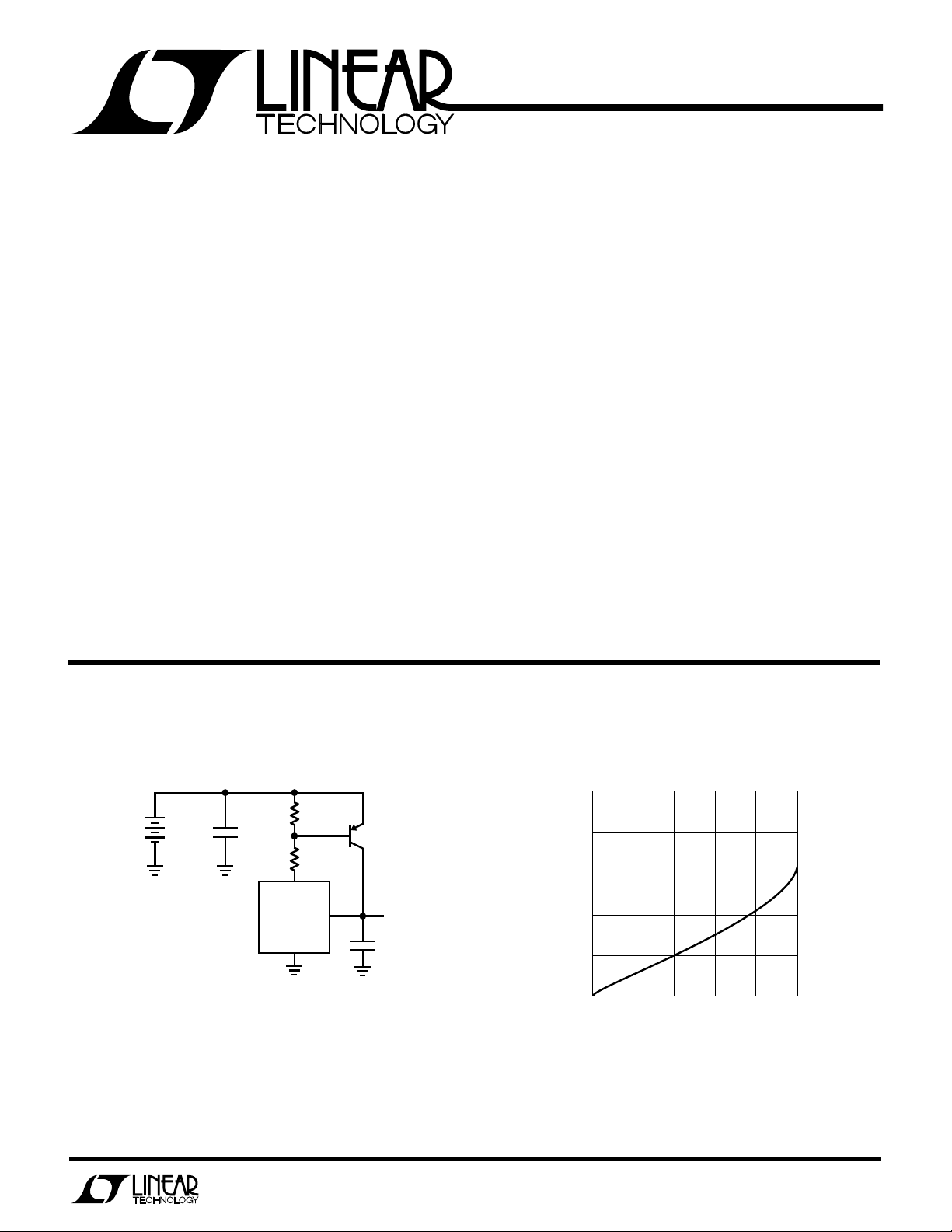
5V Low Dropout Regulator Dropout Voltage
SEALED
LEAD ACID
5.4 – 7.2V
* REQUIRED IF DEVICE IS
MORE THAN 6" FROM MAIN
FILTER CAPACITOR
†
REQUIRED FOR STABILITY
(LARGER VALUES INCREASE
STABILITY)
0.5
DRIVE
LT1123
GND
620Ω
20Ω
FB
MOTOROLA
MJE1123
+
OUTPUT = 5V/4A
†
10µF
LT1123 TA01
0.4
0.3
0.2
DROPOUT VOLTAGE (V)
0.1
0
1
0
OUTPUT CURRENT (A)
3
4
2
5
LT1123 TA02
+
10µF*
1
LT1123
WU
U
PACKAGE
/
O
RDER I FOR ATIO
W
O
A
LUTEXI T
S
Drive Pin Voltage (V
Feedback Pin Voltage (V
Operating Junction Temperature Range ... 0°C to 125°C
Storage Temperature Range ................ –65°C to 150°C
A
DRIVE
WUW
ARB
U
G
I
S
to Ground) ..................... 30V
to Ground) .................... 30V
FB
BOTTOM VIEW
3
DRIVE FB GND
ORDER PART
12
NUMBER
LT1123CZ
Lead Temperature (Soldering, 10 sec.)................ 300°C
Z PACKAGE
3-LEAD TO-92 PLASTIC
LECTRICAL C CHARA TERIST
E
PARAMETER CONDITIONS MIN TYP MAX UNITS
Feedback Voltage I
Feedback Pin Bias Current V
Drive Current VFB = 5.20V, 2V ≤ V
Drive Pin Saturation Voltage I
Line Regulation 5V < V
Load Regulation ∆I
Temperature Coefficient of V
OUT
ICS
= 10mA, TJ = 25°C 4.90 5.00 5.10 V
DRIVE
5mA ≤ I
3V ≤ V
= 5.00V, 2V ≤ V
FB
= 4.80V, V
V
FB
= 0.5V, V
V
FB
DRIVE
I
DRIVE
DRIVE
≤ 100mA
DRIVE
≤ 20V ● 4.80 5.00 5.20 V
DRIVE
≤ 15V ● 300 500 µA
DRIVE
≤ 15V ● 0.45 1.0 mA
DRIVE
= 3V ● 125 170
DRIVE
= 3V, ≤ TJ ≤ 100°C 25 100 150
DRIVE
= 10mA, VFB = 4.5V 1.4 V
= 125mA, VFB = 4.5V 2.0
< 20V ● 1.0 ±20 mV
DRIVE
= 10 to 100mA ● –5 –50 mV
0.2 mV/°C
The ● indicates specifications which apply over the full operating temperature range.
W
SPL
I
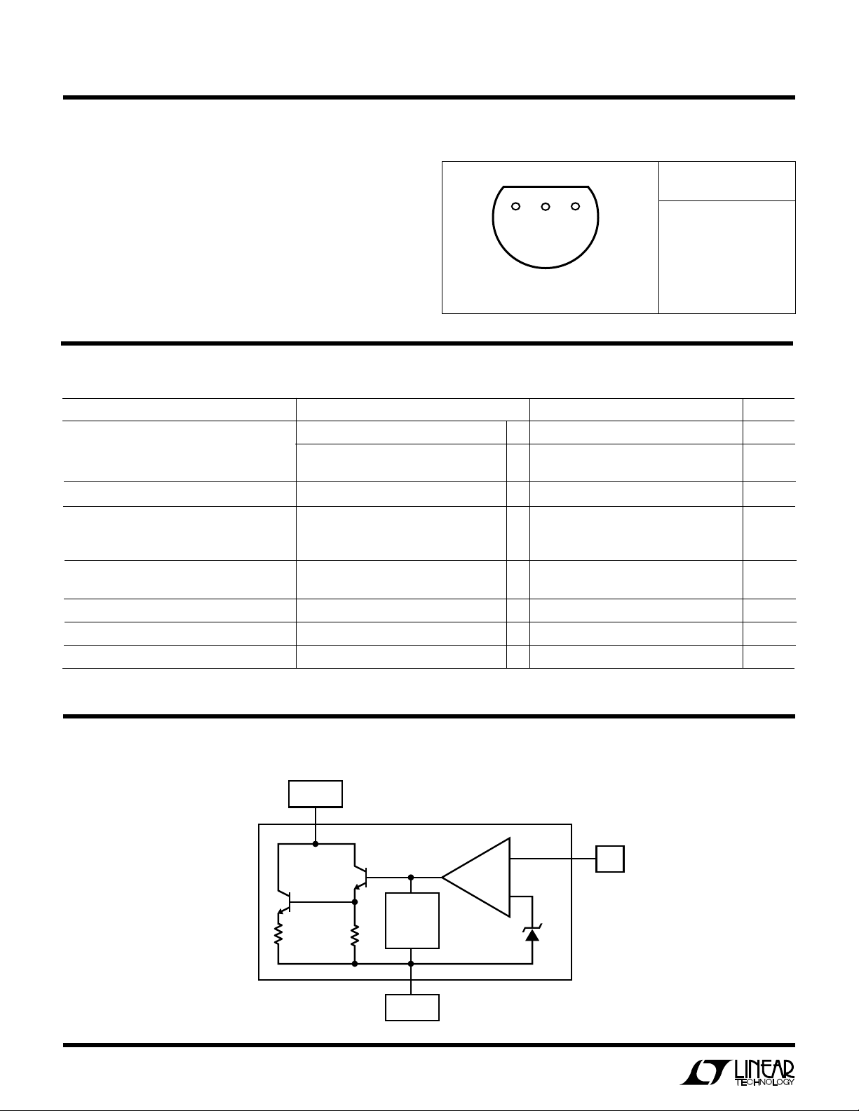
2
IIFED BLOCK
IDAGRA
W
DRIVE
CURRENT
LIMIT
THERMAL
LIMIT
GROUND
–
+
5V
FB
LT1123 SBD01
LPER
FEEDBACK PIN VOLTAGE (V)
0
0
DRIVE CURRENT (mA)
50
100
150
1234
LT1123 G03
56
200
TJ = 125°C
TJ = –50°C
TJ = 25°C
V
DRIVE
= 3V
F
O
R
ATYPICA
UW
CCHARA TERIST
E
C
LT1123
ICS
Feedback Pin Bias Current vs
Temperature
400
VFB = 5V
300
200
FEEDBACK PIN BIAS CURRENT (µA)
100
0
25 50 75 100
TEMPERATURE (°C)
Feedback Pin Bias Current vs
Feedback Pin Voltage
500
400
300
200
100
FEEDBACK PIN BIAS CURRENT (µA)
TJ = 125°C
TJ = 25°C
TJ = 0°C
LT1123 G01
125
Minimum Drive Pin Current vs
Temperature
600
V
= 3V
DRIVE
500
400
300
200
100
MINIMUM DRIVE PIN CURRENT (µA)
0
0
25 50 75 100
TEMPERATURE (°C)
Drive Pin Saturation Voltage vs
Drive Current
2.5
VFB = 4.5V
2.0
1.5
1.0
DRIVE PIN VOLTAGE (V)
0.5
TJ = 0°C
TJ = 125°C
TJ = 25°C
LT1123 G02
125
Drive Current vs Feedback Pin
Voltage
Output Voltage vs Temperature
5.03
5.02
5.01
5.00
4.99
OUTPUT VOLTAGE (V)
4.98
0
FU CTIO AL DESCRIPTIO
The LT1123 is a three pin device designed to be used in
conjunction with a discrete PNP transistor to form an
inexpensive ultra-low dropout regulator. The device incorporates a trimmed 5V bandgap reference, error amplifier,
a current-limited Darlington driver, and an internal thermal limit circuit. The internal circuitry connected to the
drive pin is designed to function at the saturation voltage
of the Darlington driver. This allows a resistor to be
1
0
FEEDBACK PIN VOLTAGE (V)
2
0
3
4
5
LT1123 G04
0
40
20
DRIVE CURRENT (mA)
80
60
100
120
LT1123 G05
140
4.97
–50
–25 0
50 100 125
25 75
TEMPERATURE (°C)
LT1123 G06
U UU
inserted in series with the drive pin. This resistor is used
to limit the base drive to the PNP and also to limit the power
dissipation in the LT1123. The value of this resistor will be
defined by the operating requirements of the regulator
circuit. The LT1123 is designed to sink a minimum of
125mA of base current. This is sufficient base drive to
form a regulator circuit which can supply output currents
up to 4A at a dropout voltage of less than 0.75V.
3

LT1123
U
UU
PI FU CTIO S
Drive Pin: The drive pin serves two functions. It provides
current to the LT1123 for its internal circuitry including
startup, bias, current limit, thermal limit and a portion of
the base drive current for the output Darlington. The sum
total of these currents (450µA typical) is equal to the
minimum drive current. This current is listed in the specifications as Drive Current with VFB = 5.2V. This is the
minimum current required by the drive pin of the LT1123.
The second function of the drive pin is to sink the base
drive current of the external PNP pass transistor. The
available drive current is specified for two conditions.
Drive current with VFB = 4.80V gives the range of current
available under nominal operating conditions, when the
device is regulating. Drive current with VFB = 0.5V gives the
range of drive current available with the feedback pin
pulled low as it would be during startup or during a short
circuit fault. The drive current available when the feedback
pin is pulled low is less than the drive current available
when the device is regulating (VFB = 5V). This can be seen
in the curve of Drive Current vs VFB Voltage in the Typical
Performance Characteristic curves. This can provide some
foldback in the current limit of the regulator circuit.
All internal circuitry connected to the drive pin is designed
to operate at the saturation voltage of the Darlington
output driver (1.4 – 2V). This allows a resistor to be
inserted between the base of the external PNP device and
the drive pin. This resistor is used to limit the base drive to
the external PNP below the value set internally by the
LT1123, and also to help limit power dissipation in the
LT1123. The operating voltage range of this pin is from
0V to 30V. Pulling this pin below ground by more than one
VBE will forward bias the substrate diode of the device.
This condition can only occur if the power supply leads are
reversed and will not damage the device if the current is
limited to less than 200mA.
Feedback Pin (VFB): The feedback pin also serves two
functions. It provides a path for the bias current of the
reference and error amplifier and contributes a portion of
the drive current for the Darlington output driver. The sum
total of these currents is the Feedback Pin Bias Current
(300µA typical). The second function of this pin is to
provide the voltage feedback to the error amplifier.
U
O
PPLICATI
A
The LT1123 is designed to be used in conjunction with an
external PNP transistor. The overall specifications of a
regulator circuit using the LT1123 and an external PNP will
be heavily dependent on the specifications of the external
PNP. While there are a wide variety of PNP transistors
available that can be used with the LT1123, the specifications given in typical transistor data sheets are of little use
in determining overall circuit performance.
Linear Technology has solved this problem by cooperating with Motorola to design and specify the MJE1123. This
transistor is specifically designed to work with the LT1123
as the pass element in a low dropout regulator. The
specifications of the MJE1123 reflect the capability of the
LT1123. For example, the dropout voltage of the MJE1123
is specified up to 4A collector current with base drive
currents that the LT1123 is capable of generating (20mA
S
I FOR ATIO
WU
U
to 120mA). Output currents up to 4A with dropout voltages less than 0.75V can be guaranteed.
The following sections describe how specifications can be
determined for the basic regulator. The charts and graphs
are based on the combined characteristics of the LT1123
and the MJE1123. Formulas are included that will enable
the user to substitute other transistors that have been
characterized. A chart is supplied that lists suggested
resistor values for the most popular range of input voltages and output current.
BASIC REGULATOR CIRCUIT
The basic regulator circuit is shown in Figure 1. The
LT1123 senses the voltage at its feedback pin and drives
the base of the PNP (MJE1123) in order to maintain the
4
 Loading...