

Linear Technology LT1120 Datasheet
FEATURES
LT1120
Micropower Regulator with
Comparator and Shutdown
U
DESCRIPTIO
■
40µA Supply Current
■
125mA Output Current
■
2.5V Reference Voltage
■
Reference Output Sources 2mA and Sinks 2mA
■
Open Collector
■
Comparator Sinks 10mA
■
Logic Shutdown
■
0.2V Dropout Voltage
■
Thermal Limiting
■
Available in 8-Lead DIP, SO and Metal Can Packages
U
APPLICATIO S
■
Battery Systems
■
Battery-Backup System
■
Portable Terminals
■
Portable Instruments
■
Memory Keep-Alive
U
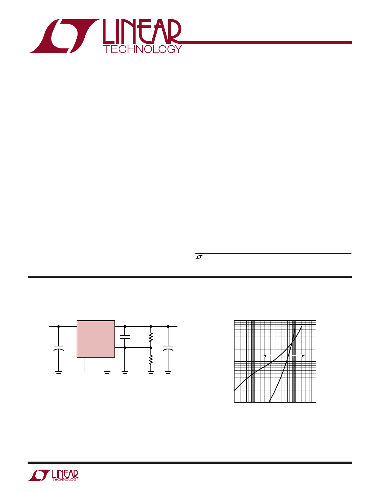
TYPICAL APPLICATIO
The LT®1120 is a combination micropower positive regulator and free collector comparator on a single monolithic
chip. With only 40µA supply current, the LT1120 can
supply over 125mA of output current. Input voltage range
is from 4.5V to 36V and dropout voltage is 0.6V at 125mA.
Dropout voltage decreases with lower load currents. Also
included on the chip is a class B output 2.5V reference that
can either source or sink current. A shutdown pin allows
logic shutdown of the output.
The comparator can be used for system or battery monitoring. For example, the comparator can be used to warn
of low system voltage. Frequency compensation of the
comparator for amplifier applications can be obtained by
adding external output capacitance.
The 2.5V reference will source or sink current. This allows
it to be used as a supply splitter or auxiliary output.
, LTC and LT are registered trademarks of Linear Technology Corporation.
V
IN
I
Q
> 5.2V
= 40µA
5V Regulator
5
V
IN
+ +
10µF
LT1120
SHUTDOWN
4
V
OUT
0.001µF1M
2
FB
GNDSHDN
13
1M
25µF
1120 TA01
Dropout Voltage and Supply Current
5V
1.00
0.10
DROPOUT VOLTAGE (V)
0.01
0.1 1
OUTPUT CURRENT (mA)
10 100 1000
10
SUPPLY CURRENT (mA)
1
0.1
1120 TA02
1
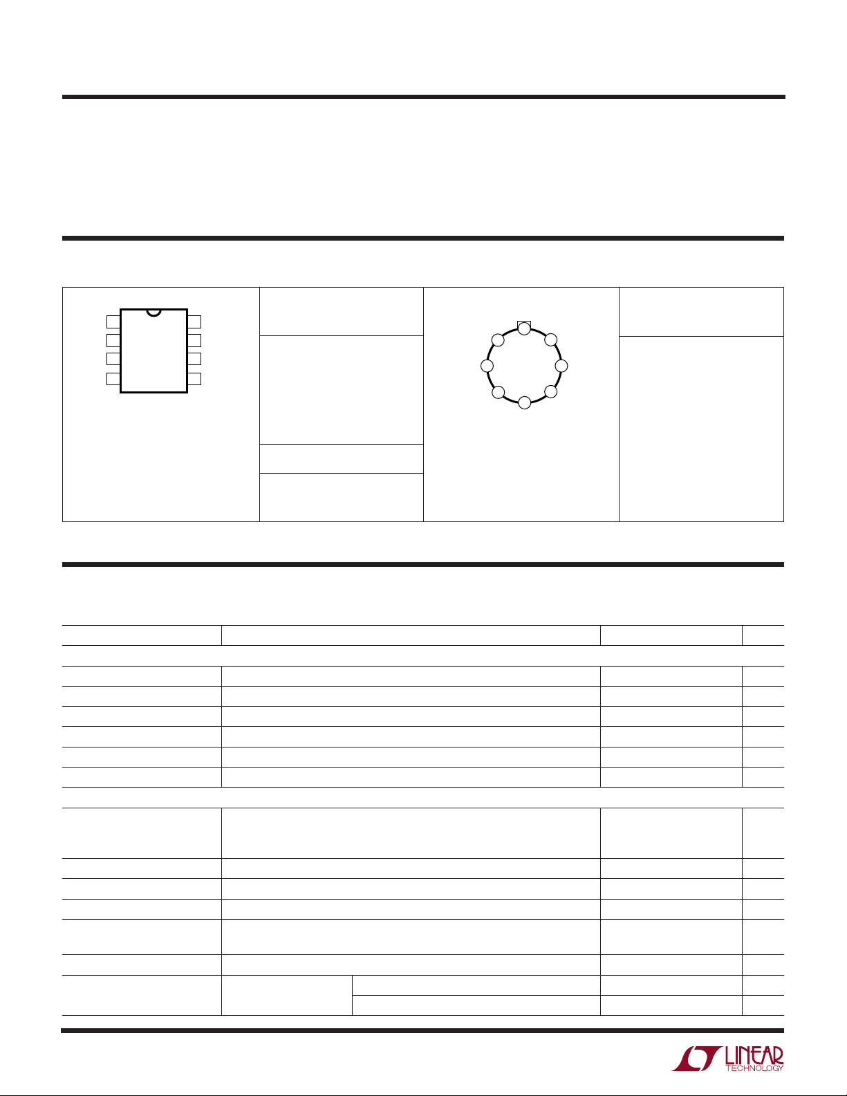
LT1120
TOP VIEW
COMPOUT
–INPUT
GND
FB REF
V
IN
SHDN
V
OUT
8
7
6
5
3
2
1
4
H PACKAGE
8-LEAD TO-5 METAL CAN
WW
W
ABSOLUTE AXI U RATI GS
U
(Note 1)
Input Voltage ........................................................... 36V
NPN Collector Voltage ............................................. 36V
Output Short-Circuit Duration.......................... Indefinite
Power Dissipation............................... Internally Limited
UUW
PACKAGE/ORDER I FOR ATIO
GND
1
FB
2
SHDN
3
V
4
OUT
J8 PACKAGE
8-LEAD CERDIP
S8 PACKAGE
8-LEAD PLASTIC SO
T
= 150°C, θJA = 100°C/W (J)
JMAX
= 110°C, θJA = 130°C/W (N)
T
JMAX
= 110°C, θJA = 150°C/W (S)
T
JMAX
TOP VIEW
N8 PACKAGE
8-LEAD PDIP
–INPUT
8
COMPOUT
7
REF
6
V
5
IN
ORDER PART
NUMBER
LT1120CJ8
LT1120CN8
LT1120CS8
LT1120IN8
LT1120IS8
S8 PART MARKING
1120
1120I
Operating Temperature Range
LT1120C................................................ 0°C to 100°C
LT1120I ................................................ –40 to 100°C
Storage Temperature Range ................. –65°C to 150°C
ORDER PART
NUMBER
LT1120CH
T
= 150°C, θJA = 150°C/W, θJC = 45°C/W
JMAX
Consult factory for Military grade parts.
ELECTRICAL CHARACTERISTICS
operating temperature range, otherwise specifications are at T
PARAMETER CONDITIONS MIN TYP MAX UNITS
Reference
Reference Voltage 4.5V ≤ VIN ≤ 36V 2.46 2.50 2.54 V
Line Regulation 4.5V ≤ VIN ≤ 36V 0.01 0.015 %/V
Load Regulation –2mA ≤ I
Output Source Current VIN = 5V 2 4 mA
Output Sink Current VIN = 5V 2 4 mA
Temperature Stability 1%
Regulator
Supply Current VIN = 6V, I
Output Current (VIN – V
Load Regulation (VIN – V
Line Regulation 6V ≤ VIN ≤ 36V 0.01 0.015 %/V
Dropout Voltage I
Feedback Sense Voltage VIN = 12V 2.44 2.5 2.56 V
Shutdown Pin Voltage Normal 0.4 V
The ● denotes the specifications which apply over the full
= 25°C. Tj = 25°C
A
≤ 2mA, VIN = 12V 0.3 0.6 %
REF
≤ 100µA4580µA
OUT
= 36V, I
V
IN
V
= 12V, I
IN
= 100µA 0.02 0.05 V
OUT
I
= 125mA 0.4 0.65 V
OUT
V
≤ 0.5V Shutdown 2.2 1.4 V
OUT
≤ 100µA 75 100 µA
OUT
= 125mA 11 20 mA
OUT
) ≥ 1V, VIN ≥ 6V 125 mA
OUT
) ≥ 1V, VIN ≥ 6V 0.2 0.5 %
OUT
2
LT1120
ELECTRICAL CHARACTERISTICS
operating temperature range, otherwise specifications are at T
PARAMETER CONDITIONS MIN TYP MAX UNITS
Shutdown Pin Current VIN = 1.4V 25 µA
Feedback Bias Current 15 40 nA
Minimum Load Current VIN = 36V 15 µA
Short-Circuit Current VIN = 36V 300 400 mA
Comparator
Offset Voltage VIN = 36V 37mV
Bias Current VIN = 36V (Note 2) 15 40 nA
Gain ∆V
Power Supply Rejection 4.5V ≤ VS ≤ 36V 80 96 dB
Output Sink Current VIN = 4.5V 10 18 mA
Saturation Voltage I
Input Voltage Range 0V
Response Time 5 µs
Leakage Current 2 µA
= 29V, RL = 20k 2000 10000 V/V
OUT
= 1mA 0.4 0.6 V
OUT
The ● denotes the specifications which apply over the full
= 25°C. Tj = 25°C
A
– 1 V
IN
ELECTRICAL CHARACTERISTICS
The ● denotes the specifications which apply over the full operating temperature range, otherwise specifications are at TA = 25°C.
PARAMETER CONDITIONS MIN TYP MAX UNITS
Reference
Reference Voltage 4.5V ≤ VIN ≤ 36V ● 2.40 2.50 2.55 V
Line Regulation 4.5V ≤ VIN ≤ 36V ● 0.01 0.02 %/V
Load Regulation –2mA ≤ I
Output Source Current VIN = 5V ● 2mA
Output Sink Current VIN = 5V ● 2mA
Regulator
Supply Current VIN = 6V, I
= 36V, I
V
IN
V
= 12V, I
IN
Output Current (VIN – V
Load Regulation (VIN – V
Line Regulation 6V ≤ VIN ≤ 36V ● 0.02 %/V
Dropout Voltage I
Feedback Sense Voltage VIN = 12V ● 2.38 2.5 2.57 V
Feedback Bias Current ● 50 nA
Minimum Load Current VIN = 36V ● 50 µA
Short-Circuit Current VIN = 36V ● 300 400 mA
OUT
I
OUT
≤ 2mA, VIN = 12V ● 0.4 0.8 %
REF
≤ 100µA ● 65 95 µA
OUT
≤ 100µA ● 85 100 µA
OUT
= 125mA ● 11 20 mA
OUT
) ≥ 1V, VIN ≥ 6V ● 125 mA
OUT
) ≥ 1V, VIN ≥ 6V ● 1%
OUT
= 100µA ● 0.06 V
= 125mA ● 0.85 V
3
LT1120
ELECTRICAL CHARACTERISTICS
The ● denotes the specifications which apply over the full operating temperature range, otherwise specifications are at TA = 25°C.
PARAMETER CONDITIONS MIN TYP MAX UNITS
Comparator
Offset Voltage ● 10 mV
Bias Current VIN = 36V (Note 2) ● 15 60 nA
Gain ∆V
Output Sink Current VIN = 4.5V (Note 3) ● 510 mA
Leakage Current VIN = 36V ● 8 µA
= 29V, RL = 20k ● 1000 V/V
OUT
Note 1: Absolute Maximum Ratings are those values beyond which the life
a device may be impaired.
Note 2: TA > 85°C, I bias maximum is 100nA.
Note 3: For TA ≤ –40°C output current sink drops to 2.5mA.
UW
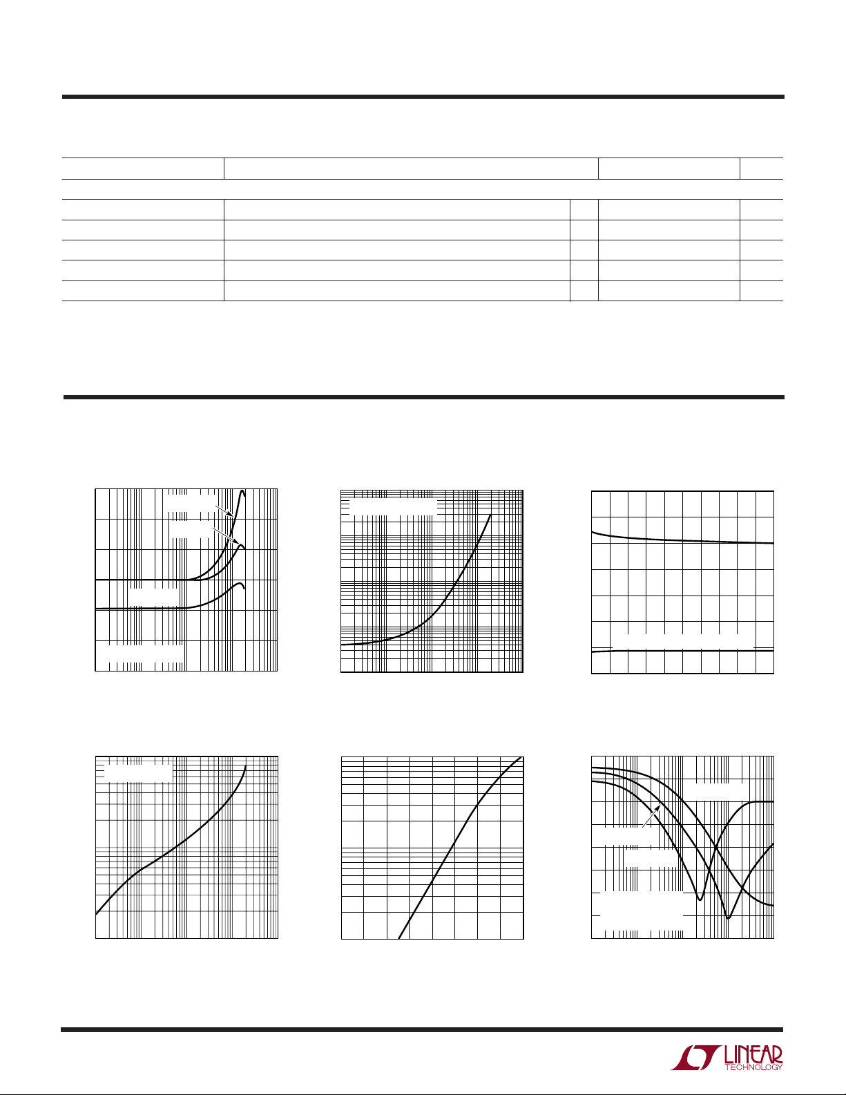
TYPICAL PERFOR A CE CHARACTERISTICS
Regulator Load Regulation Supply Current Regulator Short-Circuit Current
0.3
0.2
0.1
0
–0.1
OUTPUT VOLTAGE CHANGE (%)
–0.2
PRELOAD = 100µA
–0.3
0.1 10 100 1000
TJ = –55°C
TJ = 25°C
TJ = 125°C
1
OUTPUT CURRENT (mA)
1120 G01
100
TJ = –55°C TO 125°C
10
1
SUPPLY CURRENT (mA)
0.1
0.01
0.1 1
REGULATOR OUTPUT CURRENT (mA)
10 100 1000
1120 G02
350
300
250
200
150
100
SHORT-CIRCUIT CURRENT (mA)
CURRENT LIMIT TIED TO GROUND
50
0
–50 –10 30 70 110 150
TEMPERATURE (°C)
1120 G03
Dropout Voltage
1
∆V
= 100mV
OUT
0.1
REGULATOR INPUT-OUTPUT DIFFERENTIAL (V)
0.01
0.1 1
REGULATOR OUTPUT CURRENT (mA)
10 100 1000
4
1120 G04
Regulator Minimum Load Current Regulator Ripple Rejection
100
10
MINIMUM LOAD CURRENT (µA)
1
70 80 90 100 110 120 130 140 150
TEMPERATURE (°C)
1120 G05
70
65
60
55
I
= 10mA
OUT
50
45
RIPPLE REJECTION (dB)
40
35
30
10 1k 10k 100k
I
= 1mA
OUT
VIN = 10VDC, 1V
V
= 5V
OUT
= 10µF
C
OUT
100
RIPPLE FREQUENCY (Hz)
P–P
I
OUT
= 100mA
1120 G06
 Loading...