

Linear Technology LT1110 Datasheet
L T1110
LOAD CURRENT (mA)
0
EFFICIENCY (%)
50
60
70
80
85
90
10 20 30 40
LT1110 • TA02
75
65
55
5152535
V
IN
= 1.50V
VIN = 1.25V
VIN = 1.00V
Micropower
DC-DC Converter
Adjustable and Fixed 5V, 12V
EATU
F
■
Operates at Supply Voltages From 1.0V to 30V
■
Works in Step-Up or Step-Down Mode
■
Only Three External Off-the-Shelf Components
RE
S
Required
■
Low-Battery Detector Comparator On-Chip
■
User-Adjustable Current Limit
■
Internal 1A Power Switch
■
Fixed or Adjustable Output Voltage Versions
■
Space-Saving 8-Pin MiniDIP or S8 Package
U
O
PPLICATI
A
■
Pagers
■
Cameras
■
Single-Cell to 5V Converters
■
Battery Backup Supplies
■
Laptop and Palmtop Computers
■
Cellular Telephones
■
Portable Instruments
■
Laser Diode Drivers
■
Hand-Held Inventory Computers
S
DUESCRIPTIO
The LT1110 is a versatile micropower DC-DC converter.
The device requires only three external components to
deliver a fixed output of 5V or 12V. The very low minimum
supply voltage of 1.0V allows the use of the LT1110 in
applications where the primary power source is a single
cell. An on-chip auxiliary gain block can function as a low
battery detector or linear post regulator.
The 70kHz oscillator allows the use of surface mount
inductors and capacitors in many applications. Quiescent
current is just 300µA, making the device ideal in remote or
battery powered applications where current consumption
must be kept to a minimum.
The device can easily be configured as a step-up or
step-down converter, although for most step-down
applications or input sources greater than 3V, the LT1111
is recommended. Switch current limiting is user-adjustable
by adding a single external resistor. Unique reverse battery
protection circuitry limits reverse current to safe, nondestructive levels at reverse supply voltages up to 1.6V.
A
PPLICATITYPICAL
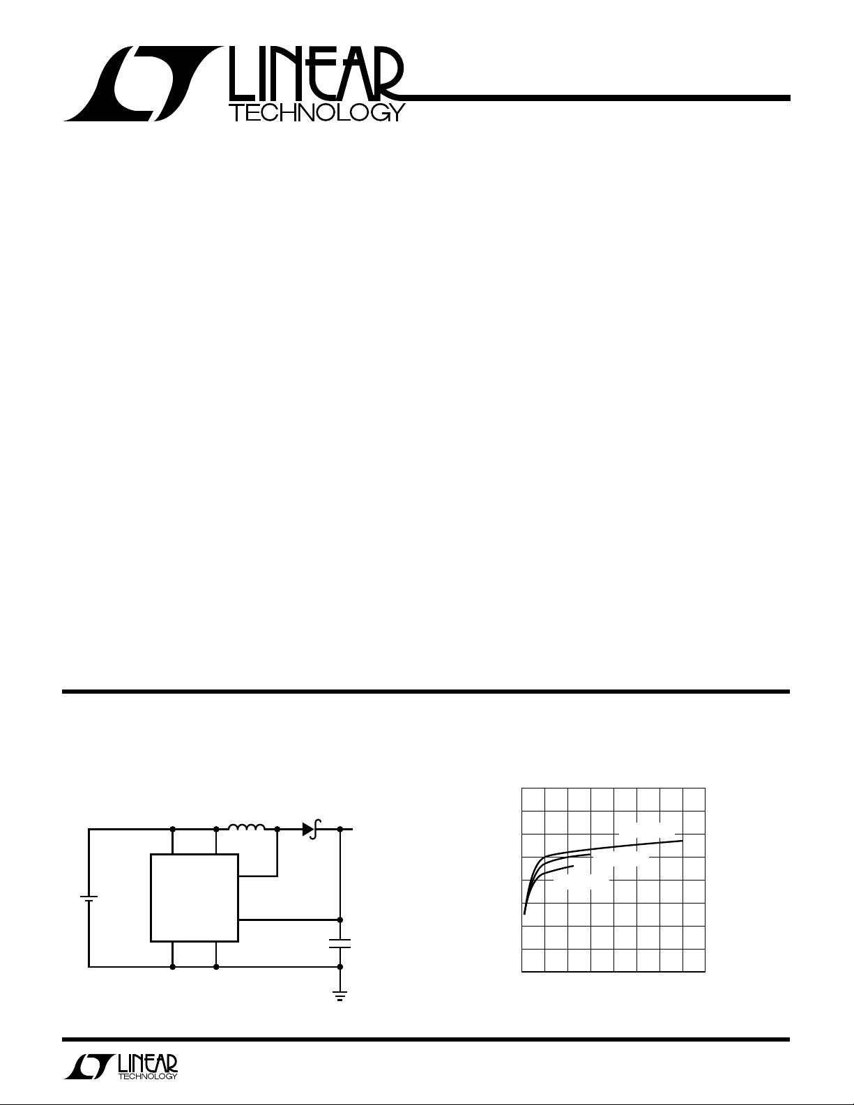
All Surface Mount
Single Cell to 5V Converter
SUMIDA
CD54-470K
47µH
1
I
LIM
1.5V
AA CELL*
OPERATES WITH CELL VOLTAGE 1.0V
*ADD 10 F DECOUPLING CAPACITOR IF BATTERY
µ
IS MORE THAN 2" AWAY FROM LT1110.
LT1110-5
GND SW2
54
V
SENSE
IN
2
SW1
≥
3
8
U
O
MBRS120T3
+
5V
15µF
TANTALUM
LT1110 • TA01
Efficiency
1
LT1110
WU
U
PACKAGE
/
O
RDER I FOR ATIO
A
W
O
LUTEXI T
S
A
WUW
ARB
U
G
I
S
Supply Voltage, Step-Up Mode................................ 15V
Supply Voltage, Step-Down Mode ........................... 36V
SW1 Pin Voltage...................................................... 50V
SW2 Pin Voltage.........................................– 0.5V to V
Feedback Pin Voltage (LT1110) .............................. 5.5V
Switch Current........................................................ 1.5A
Maximum Power Dissipation ............................. 500mW
Operating Temperature Range .....................0°C to 70°C
Storage Temperature Range ..................–65°C to 150°C
Lead Temperature (Soldering, 10 sec.).................300°C
TOP VIEW
I
1
LIM
V
2
IN
Consult factory for Industrial and Military grade parts.
IN
SW1
3
SW2
4
N8 PACKAGE
8-LEAD PLASTIC DIP
*FIXED VERSIONS
T
= 90°C, θJA = 130°C/W
JMAX
I
1
LIM
V
2
IN
SW1
3
SW2
4
S8 PACKAGE
8-LEAD PLASTIC SOIC
*FIXED VERSIONS
T
= 90°C, θJA = 150°C/W
JMAX
TOP VIEW
FB (SENSE)*
8
SET
7
A0
6
GND
5
FB (SENSE)*
8
SET
7
A0
6
GND
5
ORDER PART
NUMBER
LT1110CN8
LT1110CN8-5
LT1110CN8-12
LT1110CS8
LT1110CS8-5
LT1110CS8-12
S8 PART MARKING
1110
11105
11012
LECTRICAL C CHARA TERIST
E
SYMBOL PARAMETER CONDITIONS MIN TYP MAX UNITS
I
Q
V
IN
V
OUT
f
OSC
DC Duty Cycle Full Load (VFB < V
t
ON
I
FB
I
SET
V
AO
Quiescent Current Switch Off ● 300 µA
Input Voltage Step-Up Mode ● 1.15 12.6 V
Step-Down Mode ● 30 V
Comparator Trip Point Voltage LT1110 (Note 1) ● 210 220 230 mV
Output Sense Voltage LT1110-5 (Note 2) ● 4.75 5.00 5.25 V
LT1110-12 (Note 2) ● 11.4 12.00 12.6 V
Comparator Hysteresis LT1110 ● 48 mV
Output Hysteresis LT1110-5 ● 90 180 mV
LT1110-12 ● 200 400 mV
Oscillator Frequency ● 52 70 90 kHz
Switch ON Time ● 7.5 10 12.5 µs
Feedback Pin Bias Current LT1110, VFB = 0V ● 70 150 nA
Set Pin Bias Current V
AO Output Low I
Reference Line Regulation 1.0V ≤ VIN ≤ 1.5V ● 0.35 1.0 %/V
AO
1.5V ≤ VIN ≤ 12V ● 0.05 0.1 %/V
ICS
= V
SET
REF
= –300µA, V
TA = 25°C, VIN = 1.5V, unless otherwise noted.
1.0 12.6 V
) ● 62 69 78 %
REF
● 100 300 nA
= 150mV ● 0.15 0.4 V
SET
2
L T1110
LECTRICAL C CHARA TERIST
E
SYMBOL PARAMETER CONDITIONS MIN TYP MAX UNITS
V
CESAT
A
V
I
REV
I
LIM
I
LEAK
V
SW2
The ● denotes the specifications which apply over the full operating
temperature range.
Note 1: This specification guarantees that both the high and low trip point
of the comparator fall within the 210mV to 230mV range.
Note 2: This specification guarantees that the output voltage of the fixed
versions will always fall within the specified range. The waveform at the
sense pin will exhibit a sawtooth shape due to the comparator hysteresis.
Switch Saturation Voltage VIN = 1.5V, ISW = 400mA 300 400 mV
Step-Up Mode ● 600 mV
VIN = 1.5V, ISW = 500mA 400 550 mV
VIN = 5V, ISW = 1A 700 1000 mV
A2 Error Amp Gain RL = 100kΩ (Note 3) ● 1000 5000 V/V
Reverse Battery Current (Note 4) 750 mA
Current Limit 220Ω Between I
Current Limit Temperature – 0.3 %/°C
Coefficient
Switch OFF Leakage Current Measured at SW1 Pin 1 10 µA
Maximum Excursion Below GND I
SW1
TA = 25°C, V
ICS
LIM
≤ 10µA, Switch Off – 400 – 350 mV
= 1.5V, unless otherwise noted.
IN
● 750 mV
and V
IN
Note 3: 100kΩ resistor connected between a 5V source and the AO pin.
Note 4: The LT1110 is guaranteed to withstand continuous application of
+1.6V applied to the GND and SW2 pins while VIN, I
grounded.
400 mA
, and SW1 pins are
LIM
UW
Y
PICA
100
90
80
70
60
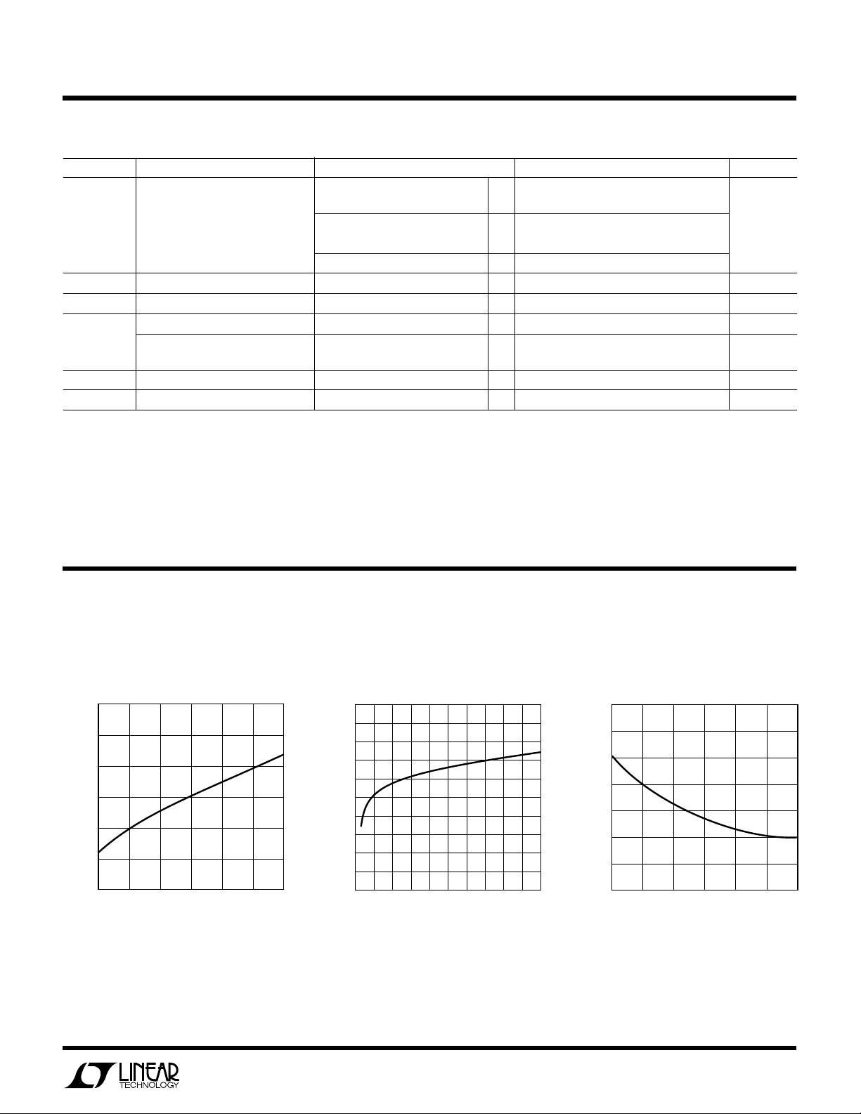
OSCILLATOR FREQUENCY (KHz)
50
40
LPER
F
O
R
AT
Oscillator Frequency Oscillator Frequency Switch On Time
–50
–25 0
TEMPERATURE (°C)
25
50
75
LT1110 • TPC01
CCHARA TERIST
E
C
80
78
76
74
72
70
68
FREQUENCY (KHz)
66
64
62
100
60
36
0
ICS
15 18 21
912
INPUT VOLTAGE (V)
242730
LT1110 • TPC02
14
13
12
11
10
ON TIME (µs)
9
8
7
–50 –25 0 25
50 75 100
TEMPERATURE (°C)
LT1110 • TPC03
3
LT1110
I (A)
0
0
V (V)
0.2
0.4
0.6
1.2
1.4
0.2 0.4 0.8 1.2
LT1110 • TPC06
1.0
1.4 1.6
SWITCH
CESAT
V
IN
= 1.0V
V = 1.2V
IN
V
IN
= 1.5V
V
IN
= 5.0V
V = 2.0V
IN
0.6 1.0
0.8
V
IN
= 3.0V
INPUT VOLTAGE (V)
QUIESCENT CURRENT (µA)
0
LT1110 • TPC09
3
400
380
360
340
320
280
260
6
240
220
200
300
912151821242730
R
LIM
(Ω)
SWITCH CURRENT (A)
10
LT1110 • TPC12
100
1.5
1.3
1.1
0.9
1000
0.7
0.5
0.3
0.1
STEP-DOWN MODE
V
IN
= 12V
UW
Y
PICA
78
76
74
72
70
68
66
DUTY CYCLE (%)
64
62
60
58
–50 –25 0 25
1.4
1.2
1.0
0.8
0.6
ON VOLTAGE (V)
0.4
0.2
0
LPER
F
O
R
AT
CCHARA TERIST
E
C
ICS
Saturation Voltage
Duty Cycle Switch Saturation Voltage Step-Up Mode
50 75 100
TEMPERATURE (°C)
LT1110 • TPC04
500
VIN = 1.5V
450
400
350
300
(mV)
250
CESAT
200
V
150
100
50
0
= 500mA
I
SW
–50 – 25 0 25
50 75 100
TEMPERATURE (°C)
LT1110 • TPC05
Switch On Voltage Minimum/Maximum Frequency vs
Step-Down Mode On Time Quiescent Current
VIN = 12V
0 0.2 0.4 0.6
I
(A)
SWITCH
0.8 1.0
LT1110 • TPC07
100
95
90
85
80
75
70
65
60
55
OSCILLATOR FREQUENCY (KHz)
50
45
40
7
9
8
10
SWITCH ON TIME (µs)
0°C ≤ TA ≤ 70°C
11
12
LT1110 • TPC08
13
500
450
400
350
300
250
200
QUIESCENT CURRENT (µA)
150
100
–50
4
Quiescent Current R
–25
0 25 50 75 100
TEMPERATURE (°C)
LT1110 • TPC10
1.5
1.3
1.1
0.9
0.7
0.5
SWITCH CURRENT (A)
0.3
0.1
Maximum Switch Current vs Maximum Switch Current vs
Step-Up R
LIM
STEP-UP MODE
≤ 5V
V
IN
10
100
R
(Ω)
LIM
1000
LT1110 • TPC11
Step-Down
LIM
UW
Y
PICA
160
140
120
100
80
60
BIAS CURRENT (nA)
40
20
0
–50
LPER
Set Pin Bias Current FB Pin Bias Current Reference Voltage
–25
0 25 50 75 100
TEMPERATURE (°C)
F
O
R
AT
LT1110 • TPC13
CCHARA TERIST
E
C
120
110
100
90
80
70
60
50
40
BIAS CURRENT (nA)
30
20
10
0
–25
–50
ICS
0 25 50 75 100
TEMPERATURE (°C)
LT1110 • TPC14
226
224
222
220
(mV)
REF
218
V
216
214
212
–50 –25 0 25
50 75 100
TEMPERATURE (°C)
L T1110
LT1110 • TPC15
U
PI
I
FUUC
(Pin 1): Connect this pin to VIN for normal use. Where
LIM
TI
O
U
S
lower current limit is desired, connect a resistor between
I
and VIN. A 220Ω resistor will limit the switch current
LIM
to approximately 400mA.
V
(Pin 2): Input supply voltage.
IN
SW1 (Pin 3): Collector of power transistor. For step-up
mode connect to inductor/diode. For step-down mode
connect to VIN.
SW2 (Pin 4): Emitter of power transistor. For step-up
mode connect to ground. For step-down mode connect to
inductor/diode. This pin must never be allowed to go more
than a Schottky diode drop below ground.
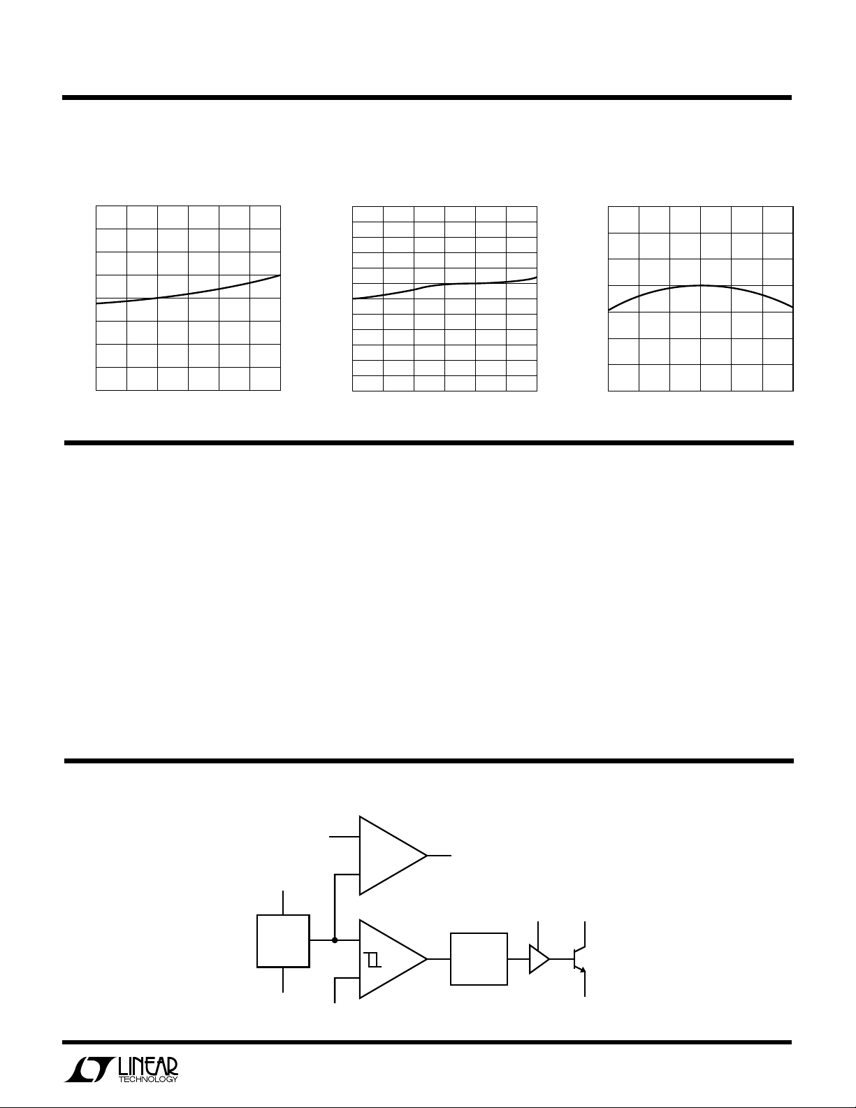
W
LT
1110
BLOCK
IDAGRA
V
IN
SET
+
A2
–
GAIN BLOCK/ERROR AMP
GND (Pin 5): Ground.
AO (Pin 6): Auxiliary Gain Block (GB) output. Open collector,
can sink 300µA.
SET (Pin 7): GB input. GB is an op amp with positive input
connected to SET pin and negative input connected to
220mV reference.
FB/SENSE (Pin 8): On the LT1110 (adjustable) this pin
goes to the comparator input. On the LT1110-5 and
LT1110-12, this pin goes to the internal application resistor
that sets output voltage.
AO
220mV
REFERENCE
GND
I
LIM
A1
COMPARATOR
FB
OSCILLATOR
DRIVER
SW1
Q1
SW2
LT1110 • BD01
5
 Loading...