

Linear Technology LT1108 Datasheet
LT1108
Micropower
DC/DC Converter
Adjustable and Fixed 5V, 12V
EATU
F
■
Operates at Supply Voltages from 2V to 30V
■
Consumes Only 110µA Supply Current
■
Works in Step-Up or Step-Down Mode
■
Only Four External Components Required
■
Low Battery Detector Comparator On-Chip
■
User Adjustable Current Limit
■
Internal 1A Power Switch
■
Fixed or Adjustable Output Voltage Versions
■
Space Saving 8-Pin MiniDIP or S8 Package
PPLICATI
A
■
Palmtop Computers
■
3V to 5V, 5V to 12V Converters
■
9V to 5V, 12V to 5V Converters
■
LCD Bias Generators
■
Peripherals and Add-On Cards
■
Battery Backup Supplies
■
Cellular Telephones
■
Portable Instruments
RE
S
O
U
S
DUESCRIPTIO
The LT1108 is a versatile micropower DC/DC converter.
The device requires only four external components to
deliver a fixed output of 5V or 12V. Supply voltage ranges
from 2V to 12V in step-up mode and to 30V in step-down
mode. The LT1108 functions equally well in step-up, stepdown, or inverting applications.
The LT1108 is pin-for-pin compatible with the LT1173, but
has a duty cycle of 70%, resulting in increased output
current in many applications. The LT1108 can deliver
150mA at 5V from a 2 AA cell input and 5V at 300mA from
9V in step-down mode. Quiescent current is just 110µA,
making the LT1108 ideal for power conscious batteryoperated systems.
Switch current limit can be programmed with a single
resistor. An auxiliary gain block can be configured as a low
battery detector, linear post regulator, undervoltage lockout circuit, or error amplifier.
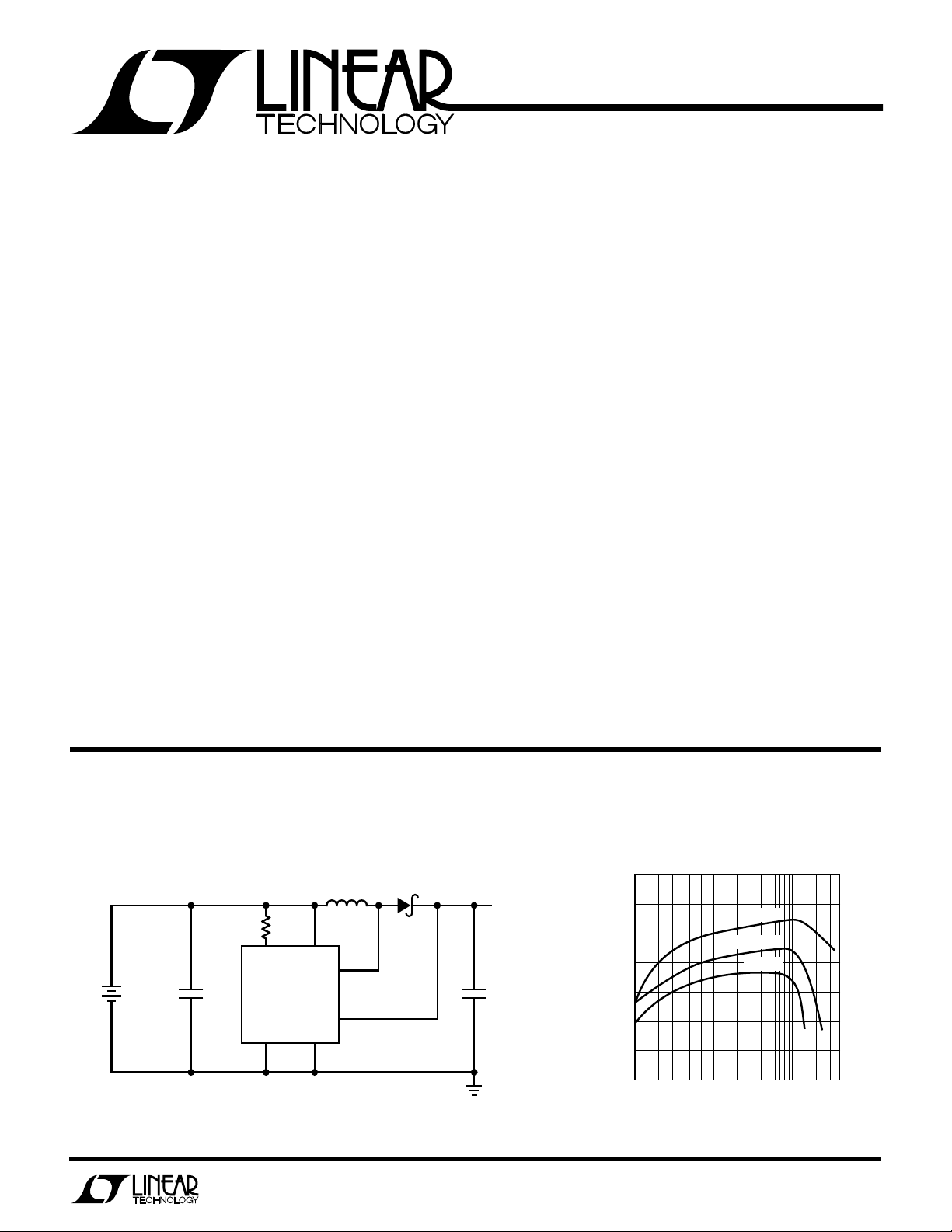
A
2 × AA
CELLS
*L1 =
+
GOWANDA GA20-103K
COILTRONICS CTX100-4
SUMIDA CD105-101K
U
O
PPLICATITYPICAL
EfficiencyPalmtop Computer Logic Supply
84
82
80
78
76
EFFICIENCY (%)
74
72
70
1
VIN = 3V
VIN = 2.5V
V
= 2V
IN
10 100
LOAD CURRENT (mA)
LT1108 • TA02
100µF
47Ω
I
LIM
GND SW2
V
LT1108-5
SENSE
IN
SW1
L1*
100µH
1N5817
+
5V
150mA
AVX
TPS
330µF
6.3V
LT1108 • TA01
1
LT1108
A
W
O
LUTEXI T
S
A
WUW
ARB
U
G
I
S
Supply Voltage (VIN)............................................... 36V
SW1 Pin Voltage (V
SW2 Pin Voltage (V
) ......................................... 50V
SW1
) ............................ –0.5V to V
SW2
Feedback Pin Voltage (LT1108) ............................. 5.5V
Sense Pin Voltage (LT1108, -5, -12) ...................... 36V
WU
/
PACKAGE
I
LIM
V
IN
SW1
SW2
T
JMAX
O
RDER I FOR ATIO
TOP VIEW
1
2
3
4
N8 PACKAGE
8-LEAD PLASTIC DIP
*FIXED VERSIONS
= 90°C, θJA = 130°C/W
FB (SENSE*)
8
SET
7
A0
6
GND
5
ORDER PART
NUMBER
LT1108CN8
LT1108CN8-5
LT1108CN8-12
Maximum Power Dissipation ............................ 500mW
Maximum Switch Current ...................................... 1.5A
Operating Temperature Range .................... 0°C to 70°C
IN
Storage Temperature Range ................ –65°C to 150°C
Lead Temperature (Soldering, 10 sec)................. 300°C
U
ORDER PART
I
1
LIM
V
2
IN
SW1
3
SW2
4
S8 PACKAGE
8-LEAD PLASTIC SOIC
*FIXED VERSIONS
T
= 90°C, θJA = 150°C/W
JMAX
TOP VIEW
FB (SENSE*)
8
SET
7
A0
6
GND
5
NUMBER
LT1108CS8
LT1108CS8-5
LT1108CS8-12
S8 PART MARKING
1108
10805
10812
LECTRICAL C CHARA TERIST
E
SYMBOL PARAMETER CONDITIONS MIN TYP MAX UNITS
I
V
V
f
t
V
V
Q
IN
OUT
OSC
ON
OL
SAT
Quiescent Current Switch OFF ● 110 150 µA
Quiescent Current, Boost Mode Configuration No Load LT1108-5 135 µA
Input Voltage Step-Up Mode ● 2 12.6 V
Comparator Trip Point Voltage LT1108 (Note 1) ● 1.2 1.245 1.3 V
Output Sense Voltage LT1108-5 (Note 2) ● 4.75 5 5.25 V
Comparator Hysteresis LT1108 ● 510 mV
Output Hysteresis LT1108-5 ● 20 40 mV
Oscillator Frequency ● 14 19 25 kHz
Duty Cycle Full Load, Step-Up Mode ● 63 70 78 %
Switch-ON Time I
Feedback Pin Bias Current LT1108, VFB = 0V ● 10 50 nA
Set Pin Bias Current V
Gain Block Output Low I
Reference Line Regulation 2V ≤ VIN ≤ 5V ● 0.20 0.400 %/V
SW
Voltage, Step-Up Mode VIN = 3V, ISW = 650mA ● 0.5 0.65 V
SAT
ICS
TA = 25°C, VIN = 3V, unless otherwise noted.
LT1108-12 250 µA
Step-Down Mode ● 30.0 V
LT1108-12 (Note 2) ● 11.4 12 12.6 V
LT1108-12
Tied to VIN, Step-Up Mode ● 28 36 48 µs
LIM
= V
SET
REF
= 100µA, V
SINK
5V ≤ V
≤ 30V ● 0.02 0.075 %/V
IN
VIN = 5V, ISW = 1A 0.8 1.00 V
= 1V ● 0.15 0.4 V
SET
● 50 100 mV
● 20 100 nA
2
LT1108
R
LIM
(Ω)
10
SWITCH CURRENT (mA)
100 1000
LT1108 • TPC03
1000
1200
1100
900
800
700
600
500
400
300
200
100
2V ≤ VIN ≤ 5V
LECTRICAL C CHARA TERIST
E
ICS
TA = 25°C, VIN = 3V, unless otherwise noted.
SYMBOL PARAMETER CONDITIONS MIN TYP MAX UNITS
V
SAT
A
V
SW
Voltage, Step-Down Mode VIN = 12V, ISW = 650mA 1.1 1.5 V
SAT
● 1.7 V
Gain Block Gain RL = 100k (Note 3) ● 400 1000 V/V
Current Limit 220Ω from I
LIM
to V
IN
400 mA
Current Limit Temperature Coefficient ● –0.3 %/°C
Switch OFF Leakage Current Measured at SW1 Pin 1 10 µA
V
SW2
● denotes specifications which apply over the full operating
The
temperature range.
Note 1: This specification guarantees that both the high and low trip points
of the comparator fall within the 1.2V to 1.3V range.
Maximum Excursion Below GND I
≤ 10µA, Switch OFF –400 –350 mV
SW1
Note 2: The output voltage waveform will exhibit a sawtooth shape due to
the comparator hysteresis. The output voltage on the fixed output versions
will always be within the specified range.
Note 3: 100k resistor connected between a 5V source and the A0 pin.
UW
Y
PICA
1.2
LPER
F
O
R
AT
Saturation Voltage Step-Up Mode
(SW2 Pin Grounded)
CCHARA TERIST
E
C
Switch ON Voltage
Step-Down Mode
(SW1 Pin Connected to VIN)
1.4
ICS
Maximum Switch Current
vs R
LIM
1.0
0.8
(V)
0.6
CESAT
V
0.4
0.2
0
0
Saturation Voltage Step-Up Mode
(SW2 Pin Grounded)
1000
900
800
700
600
500
400
300
SWITCH CURRENT (mA)
200
100
0
100
VIN = 3V
VIN = 2V
0.4 0.6 0.8
0.2
SWITCH CURRENT (A)
VIN = 24V
L = 500µH
VIN = 12V
L = 250µH
R
(Ω)
LIM
VIN = 5V
1.0 1.2
LT1108 • TPC01
V
= 5V
OUT
LT1108 • TPC04
1000
1.3
1.2
1.1
1.0
0.9
SWITCH ON VOLTAGE (V)
0.8
0.7
0.1 0.3 0.7
0.2 0.4 0.8
0
SWITCH CURRENT (A)
0.5
0.6
LT1108 • TPC02
Supply Current vs Switch Current Quiescent Current
50
40
30
20
SUPPLY CURRENT (mA)
10
0
VIN = 5V
200
0
SWITCH CURRENT (mA)
VIN = 2V
400
600
800
LTC1108 • TPC05
1000
120
115
110
105
100
95
90
QUIESCENT CURRENT (µA)
85
80
–25 0 50
–50
25
TEMPERATURE (°C)
75
LT1108 • TPC06
3
100
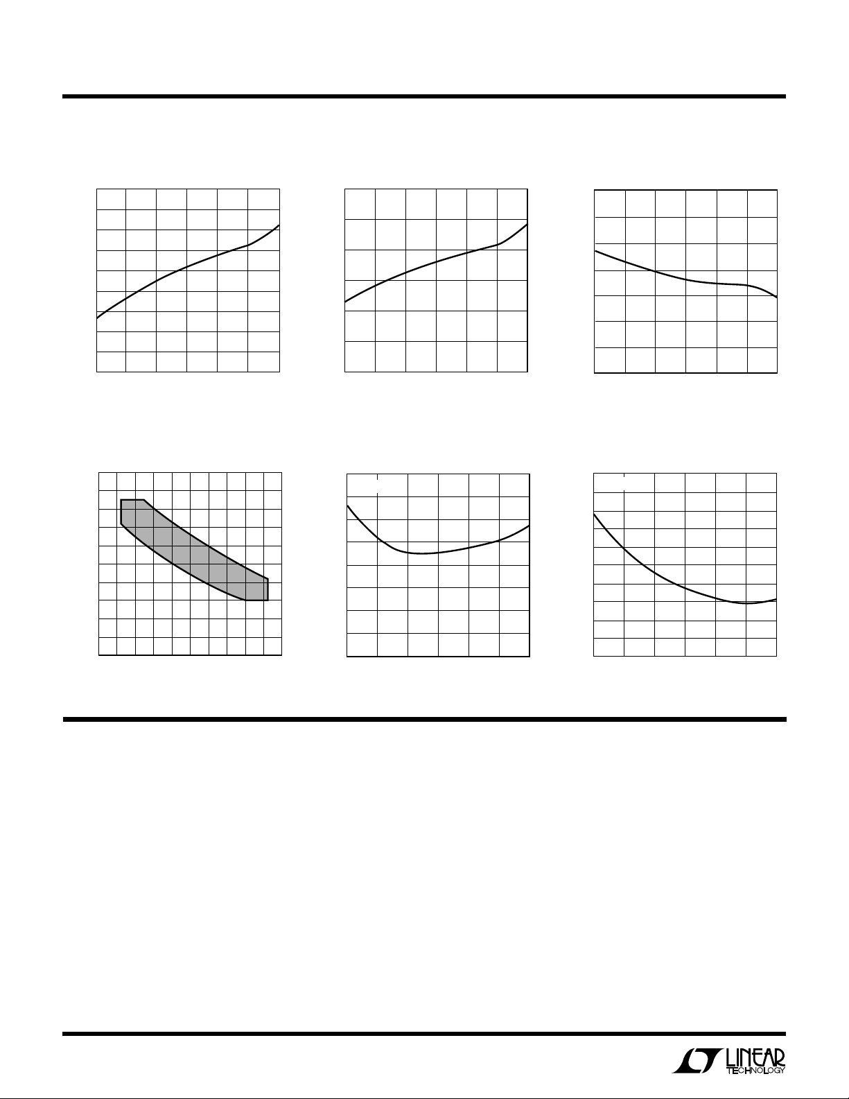
LT1108
TEMPERATURE (˚C)
–50
38
40
42
25 75
LT1108 • TPC09
36
34
–25 0
50 100
32
30
SWITCH-ON TIME (µs)
44
Y
PICA
LPER
F
O
R
AT
UW
CCHARA TERIST
E
C
ICS
Oscillator Frequency Duty Cycle Switch-ON Time
22
21
20
19
18
17
16
FREQUENCY (kHz)
15
14
13
–25 0 50
–50
25
TEMPERATURE (°C)
75
LT1108 • TPC07
100
80
75
70
65
DUTY CYCLE (%)
60
55
50
–25 0 50
–50
25
TEMPERATURE (°C)
75
LT1108 • TPC08
100
Minimum/Maximum Frequency Switch Saturation Voltage Switch Saturation Voltage
vs ON-Time Step-Up Mode Step-Down Mode
28
26
24
22
20
18
16
FREQUENCY (kHz)
14
12
10
0
30
25
40
35
ON-TIME (µs)
45
LT1108 • TPC10
0.8
ISW = 650mA
0.7
0.6
0.5
(V)
0.4
CESAT
V
0.3
0.2
0.1
50
0
–25 0 50
–50
25
TEMPERATURE (°C)
75
LT1108 • TPC11
100
(V)
SAT
V
1.8
1.6
1.5
1.4
1.2
0.8
1.7
1.3
1.1
1.0
0.9
–50
ISW = 650mA
–25
0
TEMPERATURE (°C)
25 50
75
LT1108 • TPC12
100
U
PI
I
lower current limit is desired, connect a resistor between
I
to approximately 400mA.
V
SW1 (Pin 3): Collector of power transistor. For step-up
mode connect to inductor/diode. For step-down mode
connect to VIN.
SW2 (Pin 4): Emitter of power transistor. For step-up
mode connect to ground. For step-down mode connect to
inductor/diode. This pin must never be allowed to go more
FUUC
(Pin 1): Connect this pin to VIN for normal use. Where
LIM
and VIN. A 220Ω resistor will limit the switch current
LIM
(Pin 2): Input supply voltage.
IN
TI
O
U
S
GND (Pin 5): Ground.
AO (Pin 6): Auxiliary gain block (GB) output. Open collector,
can sink 100µA.
SET (Pin 7): GB input. GB is an op amp with positive input
connected to SET pin and negative input connected to
1.245V reference.
FB/SENSE (Pin 8): On the LT1108 (adjustable) this pin
goes to the comparator input. On the LT1108-5 and
LT1108-12, this pin goes to the internal application resistor
that sets output voltage.
than a Schottky diode drop below ground.
4
 Loading...