


LT1106
LOAD CURRENT (mA)
1
70
EFFICIENCY (%)
72
74
76
78
86
10 100
LT1106 • TA02
80
82
84
VIN = 5V
VIN = 5V
VIN = 3.3V
VIN = 3.3V
D1 = MBR0530
D1 = 4 BAT54Cs
IN PARALLEL
Micropower Step-Up
DC/DC Converter for
PCMCIA Card Flash Memory
EATU
F
■
60mA Output Current at 12V from 3V Supply
■
Shutdown to 10µA
■
Programmable 12V or 5V Output
■
Up to 85% Efficiency
■
Quiescent Current: 750µA
■
Low V
■
Uses Low Value, Thin, Surface Mount Inductors
■
Ultra-Thin 20-Lead TSSOP Package
PPLICATI
A
■
PCMCIA Card Flash Memory VPP Generator
■
Portable Computers
■
Portable Instruments
■
DC/DC Converter Module Replacements
S
RE
Switch: 300mV at 0.5A Typical
CESAT
U
O
S
DUESCRIPTIO
The LT®1106 is the industry’s first DC/DC converter
designed for use on Type I and Type II PCMCIA cards. The
device senses the VPP1 and VPP2 lines at the PCMCIA
socket and generates a regulated 12V, 60mA programming supply if the socket does not provide it. Internal logic
simplifies the interface to PCMCIA card microcontrollers.
One input selects a 12V or 5V regulated output, while
another input controls micropower shutdown. Two logic
outputs indicate when the selected programming voltage
is valid and whether the input supply is 3.3V or 5V.
The regulator features Burst ModeTM operation with a 0.5A,
300mV switch for efficiency up to 85%. High frequency
500kHz switching permits the use of small value, flat
inductors that fit neatly on PCMCIA cards. The device
requires just 1µF of output capacitance.
Quiescent current is 750µA which drops to 350µA when
the card runs off the socket supply. The shutdown pin
reduces supply current to only 10µ A. The device includes
a soft start feature which limits supply current transients
when the card is inserted into a hot socket.
, LTC and LT are registered trademarks of Linear Technology Corporation.
Burst Mode is a trademark of Linear Technology Corporation.
V
CC
3.3V/5V
+
VPP1
VPP2
DALE ILS-3825-01 OR
*
COILTRONICS CTX02-11238-3
MOTOROLA MBR0530
**
U
O
A
PPLICATITYPICAL
12V, 60mA Flash Memory Programming Supply
4.7µF
TANT
ALUM
0.1µF
0.1µF
POWER ON
D
BSS84
S
0.1µF
BSS84
L1*
10µH
V
CC
VPP1
D
G1
LT1106
S
VPP2
G2
ON/OFF
VPP VALID
3/5 DETECT
SOFT START
GNDPGND
SW
AVPP
12/5
D1**
1M 0.1µF
1µF
470pF
LT1106 • TA01
12V Output Efficiency
12V/60mA
VPP VALID
3/5
1
LT1106
A
W
O
LUTEXI T
S
A
WUW
ARB
U
G
I
S
VCC Voltage............................................................... 7V
VSW Voltage............................................................ 20V
AVPP Voltage ......................................................... 20V
VPP1, VPP2 Voltage ............................................... 20V
G1, G2 Voltage ....................................................... 20V
V
V
I
LIM
Voltage......................................................... 7V
ON/OFF
Voltage ............................................................. 7V
SEL
Voltage .............................................................. 7V
Maximum Power Dissipation ............................ 500mW
Operating Temperature Range ..................... 0°C to 70°C
Storage Temperature Range ................. – 65°C to 150°C
Lead Temperature (Soldering, 10 sec).................. 300°C
LECTRICAL C CHARA TERIST
E
ICS
TA = 25°C, VCC = 5V, V
/
PACKAGE
SELECT 12/5
SOFT START
V
CC
V
CC
3/5
PGND
PGND
NC
V
SW
V
SW
T
Consult factory for Industrial and Military grade parts
O
RDER I FOR ATIO
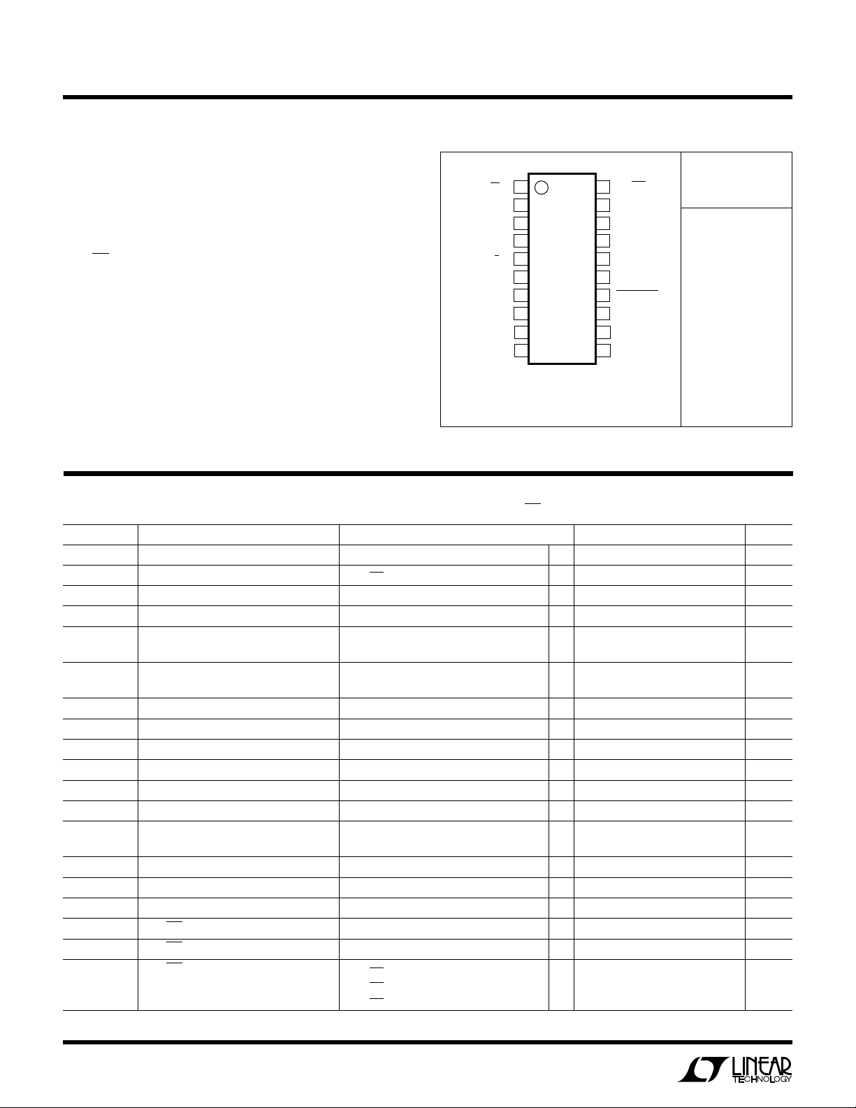
TOP VIEW
1
2
3
4
5
6
7
8
9
10
F PACKAGE
20-LEAD PLASTIC TSSOP
= 100°C, θJA = 90°C/W
JMAX
= 3V, unless otherwise noted.
ON/OFF
20
19
18
17
16
15
14
13
12
11
ON/OFF
AVPP
VPP1
VPP2
G1
G2
VPP VALID
GND
NC
V
SW
WU
ORDER PART
NUMBER
LT1106CF
U
SYMBOL PARAMETER CONDITIONS MIN TYP MAX UNITS
I
Q
f
OSC
DC Maximum Duty Cycle ● 80 85 92 %
t
ON
V
CESAT
Quiescent Current V
Quiescent Current, Shutdown V
“Doze” Mode Current V
Input Voltage Range 2 6 V
Output Sense Voltage V
Output Referred V
Comparator Hysteresis V
Oscillator Frequency Current Limit Not Asserted 400 500 700 kHz
Switch On-Time 1.7 µs
Reference Line Regulation 2V < VIN < 6V 0.06 0.15 %/V
Switch Saturation Voltage ISW = 0.5A 230 350 mV
Switch Leakage Current VSW = 12V, Switch Off 0.1 10 µA
Switch Current Limit VIN = 5V, Soft Start Floating 450 600 900 mA
Soft Start Pin Current Soft Start Grounded 80 120 µA
Select Input Voltage Low 0.8 V
Select Input Voltage High 1.6 V
ON/OFF Input Voltage Low 0.8 V
ON/OFF Input Voltage High 1.6 V
ON/OFF Bias Current V
= 0.2V, AVPP = 12V 750 900 µA
SEL
= 0.2V 9 15 µA
ON/OFF
= 0.2V, VPP1 or VPP2 = 12V 320 µA
SEL
= 3V, VPP1 and VPP2 Floating ● 4.75 5 5.25 V
SEL
= 0.2V, VPP1 and VPP2 Floating ● 11.50 12 12.60 V
V
SEL
= 3V 15 mV
SEL
= 0.2V 35 mV
SEL
= 3V, Soft Start Floating 500 650 950 mA
V
IN
= 5V 16.0 24.0 µA
ON/OFF
= 3V 8.0 14.0 µA
V
ON/OFF
= 0V 0.1 1.1 µA
V
ON/OFF
2
LT1106
LECTRICAL C CHARA TERIST
E
ICS
TA = 25°C, VCC = 5V, V
= 3V, unless otherwise noted.
ON/OFF
SYMBOL PARAMETER CONDITIONS MIN TYP MAX UNITS
Select Pin Bias Current 0V < V
< 5V 0.1 1 µA
SEL
VPP1/VPP2 Input Sense Threshold 11.0 11.5 11.9 V
AVPP Pin Input Current 50 90 µA
= 0.2V 0.1 1 µA
V
ON/OFF
VPP1/VPP2 Pin Input Current 50 90 µA
= 0.2V 0.1 1 µA
V
ON/OFF
VPP VALID Threshold AVPP Rising (High to Low Transition) ● 11.4 12 V
VPP VALID Output Voltage Low I
VPP VALID Output Voltage High I
= 100µA 0.13 0.3 V
SINK
= 2.5µA 4 4.5 V
SOURCE
3/5 Comparator Threshold ● 3.6 3.75 4.2 V
3/5 Comparator Output High I
3/5 Comparator Output Low I
= 50µA 3.65 3.8 V
LOAD
= 50µA 0.75 0.9 V
LOAD
Off State Current at G1/G2 VPP1 = 10V, VG1 = 12V or VPP2 = 10V, 0.1 1 µA
VG2 = 12V or V
ON/OFF
= 0V
The ● denotes specifications which apply over the full operating
temperature range.
W
U
TYPICAL PERFORMANCE CHARACTERISTICS
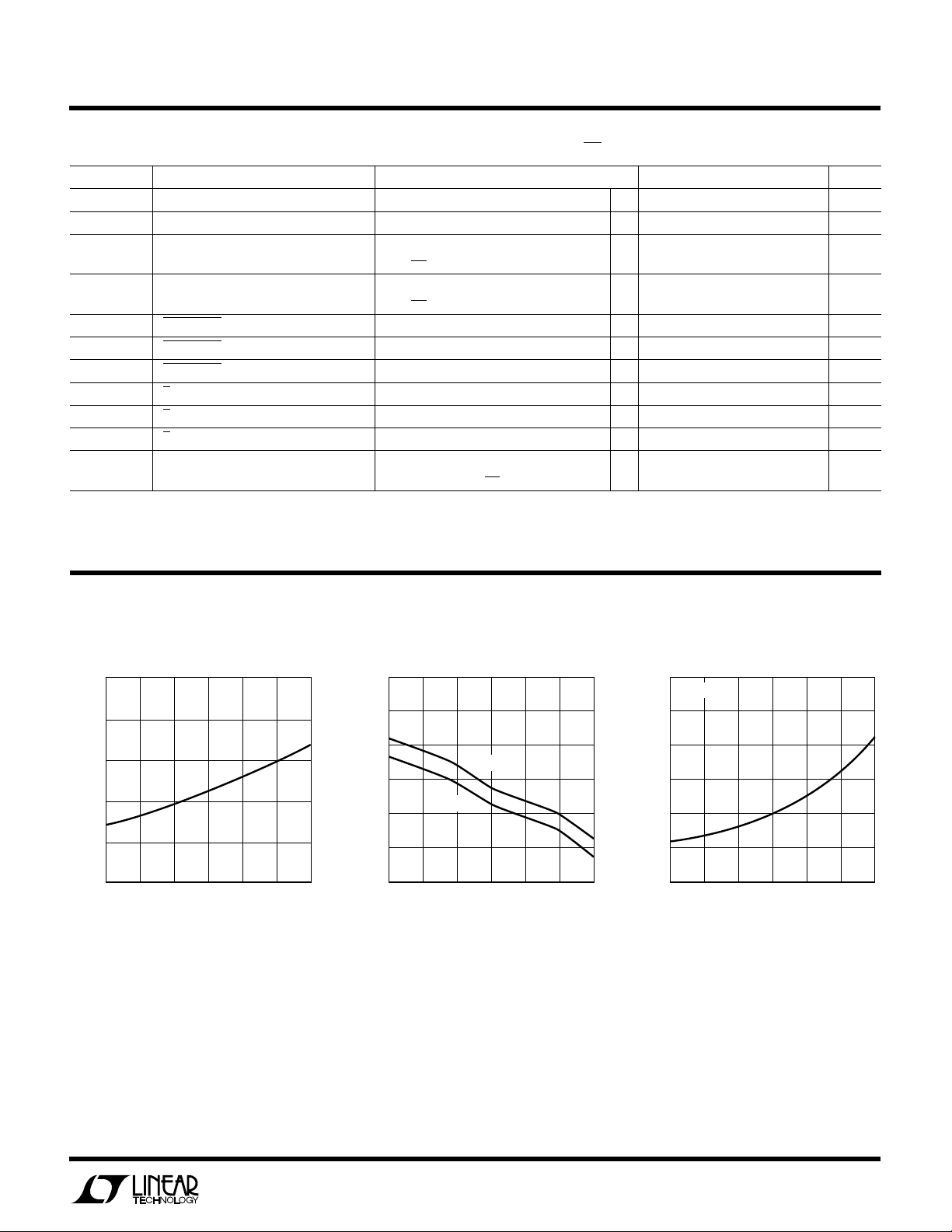
Oscillator Frequency Switch Current Limit Switch Saturation Voltage
800
700
600
500
400
OSCILLATOR FREQUENCY (kHz)
300
–50
02550
–25
TEMPERATURE (°C)
75 100
LT1106 • TPC01
1000
900
800
700
600
SWITCH CURRENT (mA)
500
400
–50
VCC = 5V
02550
–25
TEMPERATURE (°C)
VCC = 3V
75 100
LT1106 • TPC02
250
ISW = 500mA
225
200
175
150
125
SWITCH SATURATION VOLTAGE (mV)
100
–50
02550
–25
TEMPERATURE (°C)
75 100
LT1106 • TPC03
3
 Loading...