

Linear Technology LT1105IN8, LT1105IN, LT1105CN8, LT1105CN, LT1103CT7 Datasheet

OBSOLETE:
FOR INFORMATION PURPOSES ONLY
Contact Linear Technology for Potential Replacement
FEATURES
■
±1% Line and Load Regulation with No Optocoupler
■
Switch Frequency Up to 200kHz
■
Internal 2A Switch and Current Sense (LT1103)
■
Internal 1A Totem-Pole Driver (LT1105)
■
Start-Up Mode Draws Only 200µA
■
Fully Protected Against Overloads
■
Overvoltage Lockout of Main Supply
■
Protected Against Underdrive or Overdrive to FET
■
Operates in Continuous or Discontinuous Mode
■
Ideal for Flyback and Forward Topologies
■
Isolated Flyback Mode Has Fully Floating Outputs
U
APPLICATIONS
■
Up to 250W Isolated Mains Converter
■
Up to 50W Isolated Telecom Converter
■
Fully Isolated Multiple Outputs
■
Distributed Power Conversion Networks
LT1103/LT1105
Offline Switching Regulator
U
DESCRIPTION
The LT®1103 Offline Switching Regulator is designed for
high input voltage applications using an external FET
switch whose source is driven by the open collector output
of the LT1103. The LT1103 is optimized for 15W to 100W
applications. For higher power applications or additional
switch current flexibility, the LT1105 is available and its
totem pole output drives the gate of an external FET.
Unique design of the LT1103/LT1105 eliminates the need
for an optocoupler while still providing ±1% load and line
regulation in a magnetic flux-sensed converter. This significantly simplifies the design of offline power supplies
and reduces the number of components which must cross
the isolation barrier to one, the transformer.
The LT1103/LT1105 current mode switching techniques
are well suited to transformer isolated flyback and forward
topologies while providing ease of frequency compensation with a minimum of external components. Low external part count for a typical application combines with a
, LTC and LT are registered trademarks of Linear Technology Corporation.
TYPICAL APPLICATION
Fully Isolated Flyback 100kHz 50W Converter with Load Regulation Compensation
85V
TO 270V
AC
AC
+
–
BRIDGE
RECTIFIER
+
LINE
FILTER
+
220µF
385V
BAV21
13k
1%
4.75k
1%
499Ω
1000pF
18.7k
0.047µF
100Ω
BAV21
1N4148
Danger!! Lethal Voltages Present – See Text
39µF
35V
+
220k
1W
0.047µF
V
FB
GND
IN
U
DANGER!!
HIGH VOLTA
1N4148
V
SW
LT1103
15V
V
OSC
C
330Ω
0.1µF
G
390pF
E!!
1.5KE300A
5W
MUR150
BUK426-800A
10Ω
+
1µF
25V
OPTIONAL OUTPUT FILTER
MBR2045
*OUTPUT CAPACITOR IS THREE 1200µF,
50V CAPACITORS IN PARALLEL TO
ACHIEVE REQUIRED RIPPLE CURRENT
RATING AND LOW ESR.
TRANSFORMER DATA:
COILTRONICS CTX110228-3
L
= 1.6mH
(PRI)
N
PRI:NSEC
N
BIAS:NSEC
LT1103 TA13
+
*50V
3600µF
WINDINGS FOR
OPTIONAL
OUTPUTS
±12V
DC
= 1:0.05
= 1:0.27
10µH
+
50V
470µF
5V
10A
Load Regulation
5.25
5.20
5.15
5.10
5.05
(V)
5.00
OUT
V
4.95
4.90
4.85
4.80
4.75
0
270V
2
3
1
220V
AC
110V
AC
AC
579
6
4
I
OUT
8
(A)
85V
AC
LT1103 TA02
10
1

LT1103/LT1105
U
DESCRIPTION
200kHz maximum switching frequency to achieve high
power density. Performance at switching frequencies
above 100kHz may be degraded due to internal timing
constraints associated with fully isolated flyback mode.
Included are the oscillator, control, and protection circuitry such as current limit and overvoltage lockout.
Switch frequency and maximum duty cycle are adjustable.
Bootstrap circuitry draws 200µA for start-up of isolated
topologies. A 5V reference as well as a 15V gate bias are
available to power external primary-side circuitry. No
external current sense resistor is necessary with LT1103
because it is integrated with the high current switch. The
LT1105 brings out the input to the current limit amplifier
and requires the use of an external sense resistor.
The LT1103/LT1105 have unique features not found on
other offline switching regulators. Adaptive antisat switch
drive allows wide ranging load currents while maintaining
high efficiency. The external FET is protected from insufficient or excessive gate drive voltage with a drive detection circuit. An externally activated shutdown mode
reduces total supply current to less than 200µA, typical for
standby operation. Fully isolated and regulated outputs
can be generated in the optional isolated flyback mode
without the need for optocouplers or other isolated feedback paths.
U
U
WAR I G!
DANGEROUS AND LETHAL POTENTIALS ARE
PRESENT IN OFFLINE CIRCUITS!
BEFORE PROCEEDING ANY FURTHER, THE
READER IS WARNED THAT CAUTION MUST
BE USED IN THE CONSTRUCTION, TESTING
AND USE OF OFFLINE CIRCUITS. HIGH
VOLTAGE, AC LINE-CONNECTED POTENTIALS
ARE PRESENT IN THESE CIRCUITS. EXTREME
CAUTION MUST BE USED IN WORKING WITH
AND MAKING CONNECTIONS TO THESE
CIRCUITS. REPEAT: OFFLINE CIRCUITS
CONTAIN DANGEROUS, AC LINE-CONNECTED
HIGH VOLTAGE POTENTIALS. USE CAUTION.
ALL TESTING PERFORMED ON AN OFFLINE
CIRCUIT MUST BE DONE WITH AN ISOLATION
TRANSFORMER CONNECTED BETWEEN THE
OFFLINE CIRCUIT'S INPUT AND THE AC LINE.
USERS AND CONSTRUCTORS OF OFFLINE
CIRCUITS MUST OBSERVE THIS PRECAUTION
WHEN CONNECTING TEST EQUIPMENT TO
THE CIRCUIT TO AVOID ELECTRIC SHOCK.
REPEAT: AN ISOLATION TRANSFORMER
MUST BE CONNECTED BETWEEN THE CIRCUIT
INPUT AND THE AC LINE IF ANY TEST
EQUIPMENT IS TO BE CONNECTED.
WW
W
ABSOLUTE MAXIMUM RATINGS
VIN.......................................................................... 30V
V
Output Voltage (LT1103)................................. 50V
SW
VSW Output Current (200ns)(LT1105) ................. ±1.5A
VC, FB, OSC, SS ........................................................ 6V
I
(LT1105) ........................................................... 3V
LIM
0VLO Input Current ............................................... 1mA
Lead Temperature (Soldering, 10 sec.)................ 300°C
U
(Note 1)
2
Maximum Operating Ambient Temperature Range
LT1103C .............................................. 0°C to 70°C
LT1105C .............................................. 0°C to 70°C
Maximum Operating Junction Temperature Range
LT1103C ............................................. 0°C to 100°C
LT1105C ............................................ 0°C to 100°C
LT1105I ......................................... –40°C to 125°C
Storage Temperature Range ................. –65°C to 150°C
LT1103/LT1105
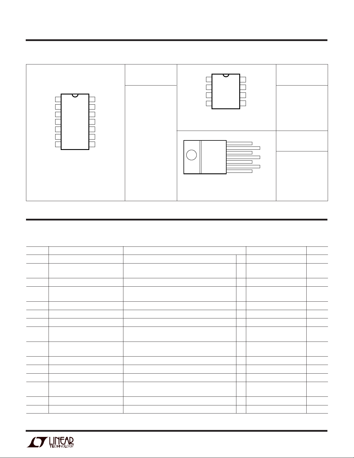
U
W
PACKAGE/ORDER INFORMATION
ORDER PART
NUMBER
TOP VIEW
PWRGND
1
2
OVLO
3
FB
4
V
C
5
5V
6
SS
7
GND
N PACKAGE
14-LEAD PDIP
PINS 1 AND 7 MUST BE TIED TOGETHER
T
= 100°C, θJA = 100°C/W
JMAX
V
14
SW
NC
13
NC
12
15V
11
V
10
IN
OSC
9
I
8
LIM
Consult factory for Military grade parts.
LT1105CN
LT1105IN
U
TOP VIEW
GND
1
I
2
LIM
3
FB
45
V
C
N8 PACKAGE
8-LEAD PDIP
T
= 100°C, θJA = 130°C/W
JMAX
FRONT VIEW
7
6
5
4
3
2
1
T7 PACKAGE
CASE IS CONNECTED TO GROUND. LEADS ARE FORMED
7-LEAD TO-220
= 100°C, θJA = 50°C/W
T
JMAX
ORDER PART
8
V
SW
15V
7
6
V
IN
OSC
NUMBER
LT1105CN8
LT1105IN8
ORDER PART
15V
V
IN
OSC
GND
V
C
FB
V
SW
NUMBER
LT1103CT7
ELECTRICAL CHARACTERISTICS
VIN = 20V, VC = 0.85V, OVLO = 0V, VSW Open, TA = 25°C, unless otherwise noted.
SYMBOL PARAMETER CONDITIONS MIN TYP MAX UNITS
I
Q
I
START
V
REF
V
GATE
SF Oscillator Scaling Factor FB = 4V, VC = Open, Measured at VSW, ISW = 25mA, 36 40 44 Hz • µF
Supply Current 8V < VIN < 30V, After Device Has Started ● 10 20 30 mA
Start-Up Current VIN < VIN Start Threshold ● 200 400 µA
Industrial Grade
● 450 µA
VIN Start Threshold ● 14.5 16.0 17.5 V
VIN Shutdown Threshold Note: Switching Stops When VSW < 10V (LT1103) ● 5.0 7.0 8.0 V
Note: Switching Stops When V
< 10V (LT1105)
GATE
5V Reference Voltage ● 4.80 4.95 5.20 V
V
Line Regulation 10V < VIN < 30V ● 0.025 0.1 %/ V
REF
V
Load Regulation 0mA < IL < 20mA ● 0.025 0.05 %/mA
REF
V
Short-Circuit Current Commercial Grade ● 25 60 110 mA
REF
Industrial Grade
● 20 120 mA
15V Short-Circuit Current Commercial Grade ● 30 130 mA
Industrial Grade
● 25 140 mA
15V Gate Bias Reference 17 < VIN < 30V, 0mA < IL < 30mA ● 13.8 15.0 16.2 V
15V Dropout Voltage VIN = 15V, IL = 30mA ● 2.0 2.5 V
15V Short-Circuit Current ● 30 70 130 mA
OVLO = 5V, f
OSC
= SF/C
OSC,
40kHz < f
< 200kHz ● 32 40 48 Hz • µF
OSC
Oscillator Valley Voltage 2.0 V
Oscillator Peak Voltage 4.5 V
3
LT1103/LT1105
ELECTRICAL CHARACTERISTICS
VIN = 20V, VC = 0.85V, OVLO = 0V, VSW Open, TA = 25°C, unless otherwise noted.
SYMBOL PARAMETER CONDITONS MIN TYP MAX UNIT
DC Preset Max Switch Duty Cycle FB = 4V, VC = Open, f
(LT1103) Note: Maximum Duty Cycle Can Be Altered at OSC Pin
Preset Max Switch Duty Cycle FB = 4V, VC = Open, f
(LT1105) Note: Maximum Duty Cycle Can Be Altered at OSC Pin
Industrial Grade ● 55 75 %
OVLO Threshold Overvoltage Lockout Threshold at Which Switching is Inhibited ● 2.3 2.5 2.7 V
Industrial Grade
OVLO Input Bias Current OVLO = 2V, Measured Out of Pin (Note 2) ● 1.0 3.0 µA
V
FB
gm Error Amp Transconductance ∆I(VC) = ±50µA 9000 12000 17500 µmho
A
V
BV Switch Breakdown Voltage ISW = 5mA ● 50 70 V
∆I
IN
∆I
SW
FB Threshold Voltage I(VC) = 0mA 4.425 4.50 4.575 V
FB Input Bias Current FB = VFB (Note 3) ● 51020 µA
Industrial Grade
Change in FB Input FB = VFB, VC = 1V to 4V (Note 3) 8 11 13 µA/V
Bias Current with Change in V
FB Threshold Line Regulation 10V < VIN < 30V ● 0.025 0.10 %/V
Error Amp Voltage Gain 1V < VC < 3V ● 500 1250 V/V
VC Switching Threshold Switch Duty Cycle = 0% ● 0.85 1.25 1.4 V
Shutdown Threshold Voltage ● 50 150 250 mV
Error Amp Source Current ● 150 275 µA
Error Amp Sink Current ● 1.5 3 4.5 mA
Error Amp Clamp Voltage FB = 4.75V ● 0.3 0.7 0.9 V
Soft-Start Charging Current SS = 0V ● 25 40 60 µA
Soft-Start Reset Current VIN = 6V, SS = 0.3V ● 12 mA
Output Switch Leakage VSW = 45V ● 500 µA
(LT1103) V
(LT1103)
VSW Current Limit (LT1103) Duty Cycle = 25% (Note 4) ● 2.0 2.5 3.0 A
Output Switch On Resistance ● 0.4 0.75 Ω
(LT1103)
IQ Increase During Switch On Time ISW = 0.5A to 1.5A ● 30 50 mA/A
(LT1103)
Switch Output High Level ISW = 200mA, V
(LT1105) I
Switch Output High Level I
Industrial Grade I
C
Industrial Grade
Industrial Grade
Industrial Grade
Industrial Grade
Industrial Grade
FB = 4.0V
Industrial Grade
= 15V ● 200 µA
SW
= 750mA, V
SW
= 200mA, V
SW
= 750mA, V
SW
= 40kHz, ISW = 25mA, ● 58 65 72 %
OSC
= 40kHz, ISW = 25mA, ● 56 63 70 %
OSC
● 2.2 2.8 V
● 4.400 4.50 4.600 V
● 422µA
● 71114 µA/V
● 615µA/V
● 6000 12000 20000 µmho
● 5000 24000 µmho
● 450 V/V
● 50 300 mV
● 0.7 4.5 mA
● 4.2 4.4 4.6 V
● 20 75 µA
= 15V ● 13.00 13.5 V
GATE
= 15V ● 12.50 13.2 V
GATE
= 15V ● 12.75 V
GATE
= 15V ● 12.25 V
GATE
4
LT1103/LT1105
ELECTRICAL CHARACTERISTICS
VIN = 20V, VC = 0.85V, OVLO = 0V, VSW Open, TA = 25°C, unless otherwise noted.
SYMBOL PARAMETER CONDITONS MIN TYP MAX UNIT
Switch Output Low Level ISW = 200mA ● 0.25 0.50 V
(LT1105) I
Rise Time (LT1105) CL = 1000pF 50 ns
Fall Time (LT1105) CL = 1000pF 20 ns
I
Threshold Voltage (LT1105) Duty Cycle = 25% (Note 5) ● 300 375 450 mV
LIM
Low Switch Drive Lockout Measured at VSW (LT1103) ● 9.0 9.5 10.5 V
Threshold Measured at 15V Gate Bias Reference (LT1105)
High Switch Drive Lockout Measured at VSW (LT1103) ● 17.0 18.5 20.0 V
Threshold Measured at 15V Gate Bias Reference (LT1105)
= 750mA ● 0.75 1.50 V
SW
The ● denotes specifications which apply over the full operating
temperature range.
Note 1: Absolute Maximum Ratings are those values beyond which the life
of a device may be impaired.
Note 2: The OVLO pin is clamped with a 5.5V Zener and can sink a
maximum input current of 1mA.
Note 3: FB input bias current changes as a function of the V
Rate of change of FB input bias current is 11µA/V of change on V
pin voltage.
C
. By
C
Note 4: Current limit on VSW is constant for DC < 35% and decreases for
DC > 35% due to internal slope compensation circuity. The LT1103 switch
current limit is given by I
Note 5: The current limit threshold voltage is constant for DC < 35% and
decreases for DC > 35% due to internal slope compensation circuitry. The
LT1105 switch current limit threshold voltage is given by V
(1.7 – DC) above 35% duty cycle.
including a resistor in series with the FB pin, load regulation can be set
to zero.
W
U
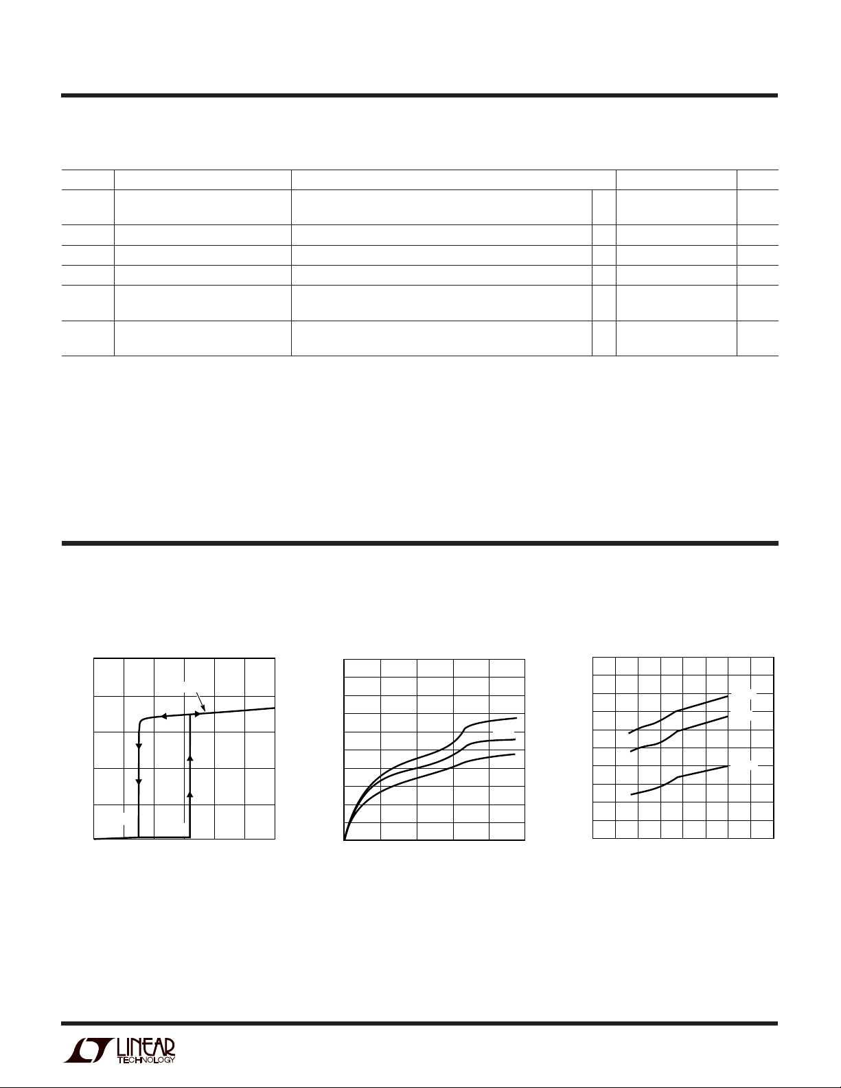
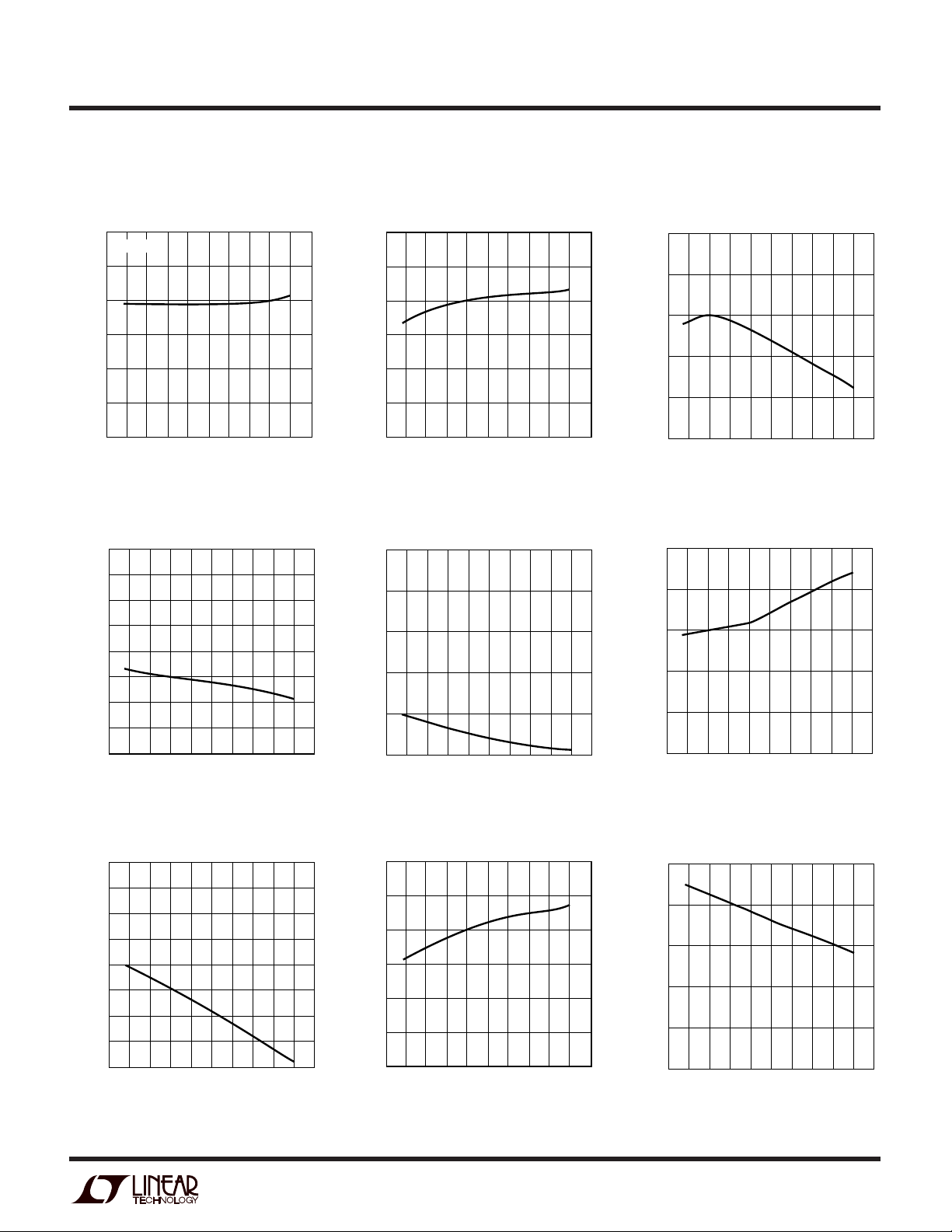
TYPICAL PERFORMANCE CHARACTERISTICS
Start-Up Supply Current vs
Supply Current vs Input Voltage
25
20
15
10
SUPPLY CURRENT (mA)
5
I
SHUT
0
0
5
25°C
I
START
10 15 20
INPUT VOLTAGE (V)
25 30
LT1103 G01
Input Voltage
500
450
400
350
300
250
200
150
100
START-UP SUPPLY CURRENT (µA)
50
0
0
125°C
–55°C
3
6
INPUT VOLTAGE (V)
9
12
25°C
LT1103 G02
1.76 (1.536 – DC) above 35% duty cycle.
LIM =
= 0.225
LIM
Quiescent Supply Current vs
Input Voltage
22
21
20
19
18
17
16
15
14
QUIESCENT SUPPLY CURRENT (mA)
13
12
0
515
15
10
20
INPUT VOLTAGE (V)
125°C
25°C
–55°C
35
30
25
40
LT1103 G03
5
LT1103/LT1105
W
U
TYPICAL PERFORMANCE CHARACTERISTICS
Quiescent Supply Current vs
Temperature
22
21
20
19
18
17
16
15
14
QUIESCENT SUPPLY CURRENT (mA)
13
12
–25
–50
–75
50 75 100 150
0
25
TEMPERATURE (°C)
VIN Start-Up Threshold vs
Temperature
17.5
17.0
16.5
16.0
15.5
START-UP THRESHOLD (V)
IN
V
15.0
30V
8V
125
LT1103 G04
175
Shutdown Supply Current vs
Input Voltage
500
450
A)
µ
400
350
300
250
200
150
100
SHUTDOWN SUPPLY CURRENT (
50
0
0
5
VC = 75mV
15
10
INPUT VOLTAGE (V)
VIN Shutdown Threshold vs
Temperature
8.0
7.7
7.4
7.1
SHUTDOWN THRESHOLD (V)
6.8
IN
V
VC = 0
20
Shutdown Supply Current vs
VC Voltage
500
450
400
350
300
250
200
150
SHUTDOWN CURRENT (µA)
100
50
30
LT1103 G05
35
25
0
0
–55°C
40
20
100 140 180
60
80
VC (mV)
25°C
120
125°C
160
200
LT1103 G06
Output Switch Frequency vs
Temperature
45
C
= 1000pF
OSC
43
41
39
37
OUTPUT SWITCH FREQUENCY (kHz)
14.5
–75
–50
0 50 100 150
–25 25 75 125
TEMPERATURE (°C)
Preset Switch Maximum Duty
Cycle vs Temperature
75
C
= 1000pF
OSC
72
69
66
63
PRESET SWITCH DUTY CYCLE (%)
60
–75
–25
25
0–50
TEMPERATURE (°C)
6
175
LT1103 G07
6.5
–75
–25
–50 0
75
25
50 100
TEMPERATURE (°C)
125
150
LT1103 G08
175
Switch Oscillator Frequency vs
Capacitance
1000
100
SWITCH FREQUENCY (kHz)
10
75
125
10050
150
LT1103 G10
175
100
1000 10000
CAPACITANCE (pF)
LT1103 G11
35
–50 0
–75
–25
TEMPERATURE (°C)
50 150
75
25
Overvoltage Lockout Threshold vs
Temperature
3.0
2.8
2.6
2.4
2.2
OVERVOLTAGE LOCKOUT THRESHOLD (V)
2.0
–75
–25
25
0–50
TEMPERATURE (°C)
75
10050
100
125
125
LT1103 G09
150
LT1103 G12
175
W
TEMPERATURE (°C)
–75
5V LINE REGULATION (%/V)
0.03
0.04
0.05
125
LT1103 G18
0.02
0.01
0
–25
25
75
175
150
10050
0–50
TEMPERATURE (°C)
–75
15V GATE BIAS DROPOUT VOLTAGE (V)
1.5
2.0
2.5
125
LT1103 G21
1.0
0.5
0
–25
25
75
175
150
10050
0–50
TEMPERATURE (°C)
–75
SOFT-START RESET CURRENT (mA)
3
4
5
125
LT1103 G15
2
1
0
–25
25
75
175
150
10050
0–50
U
TYPICAL PERFORMANCE CHARACTERISTICS
LT1103/LT1105
OVLO Input Bias Current vs
Temperature
0
OVLO = 2V
–0.5
–1.0
–1.5
–2.0
–2.5
OVLO INPUT BIAS CURRENT (µA)
–3.0
–75
–50
0 50 100 150
–25 25 75 125
TEMPERATURE (°C)
5V Reference Voltage vs
Temperature
5.20
5.15
5.10
5.05
5.00
4.95
4.90
5V REFERENCE VOLTAGE (V)
4.85
LT1103 G13
175
Soft-Start Charging Current vs
Temperature
60
50
40
30
20
10
SOFT-START CHARGING CURRENT (µA)
0
–75
–50
0 50 100 150
–25 25 75 125
TEMPERATURE (°C)
5V Load Regulation vs
Temperature
0.025
0.020
0.015
0.010
0.005
5V LOAD REGULATION (%/mA)
Soft-Start Reset Current vs
Temperature
175
LT1103 G14
5V Line Regulation vs
Temperature
4.80
–75
–50
–25
0
TEMPERATURE (°C)
5V Reference Short-Circuit
Current vs Temperature
110
100
90
80
70
60
50
40
5V REFERENCE SHORT-CIRCUIT CURRENT (mA)
30
–25
–50
0
TEMPERATURE (°C)
–75
100
50
75
25
50
75
25
100
125
125
150
LT1103 G16
150
LT1103 G19
175
175
0
–25
–75
25
0–50
TEMPERATURE (°C)
15V Gate Bias Reference vs
Temperature
16.2
15.8
15.4
15.0
14.6
15V GATE BIAS REFERENCE (V)
14.2
13.8
–75
–50
0 50 100 150
–25 25 75 125
TEMPERATURE (°C)
75
125
10050
150
LT1103 G17
175
15V Gate Bias Dropout Voltage vs
Temperature
175
LT1103 G20
7
LT1103/LT1105
W
U
TYPICAL PERFORMANCE CHARACTERISTICS
15V Gate Bias Short-Circuit
Current vs Temperature
130
110
90
70
50
30
15V GATE BIAS SHORT-CIRCUIT CURRENT (mA)
–75
–25
25
0–50
TEMPERATURE (°C)
75
125
10050
Feedback Threshold vs
Temperature
4.60
4.56
4.52
150
LT1103 G22
175
Low Switch Drive Lockout
Threshold vs Temperature
10.5
10.2
9.9
9.6
9.3
LOW SWITCH DRIVE LOCKOUT THRESHOLD (V)
9.0
–75
–25
25
0–50
TEMPERATURE (°C)
75
10050
125
FB Input Bias Current vs
Temperature (VC = 1V)
20
16
12
150
LT1103 G23
175
High Switch Drive Lockout
Threshold vs Temperature
20.0
19.5
19.0
18.5
18.0
17.5
HIGH SWITCH DRIVE LOCKOUT THRESHOLD (V)
17.0
–75
–50
0 50 100 150
–25 25 75 125
TEMPERATURE (°C)
Change in FB Input Bias Current
with Change in VC vs Temperature
(VC = 1V to 4V)
14
13
12
(µA/V)
C
11
175
LT1103 G24
4.48
FEEDBACK THRESHOLD (V)
4.44
4.40
–75
–25
25
0–50
TEMPERATURE (°C)
75
Error Amplifier Transconductance
vs Temperature
25000
20000
15000
10000
5000
ERROR AMPLIFIER TRANSCONDUCTANCE (µmho)
–75
–50 0
–25
50
75
25
TEMPERATURE (°C)
10050
100
125
125
150
LT1103 G25
150
LT1103 G28
8
4
FB INPUT BIAS CURRENT (µA)
0
–25
175
–75
25
0–50
TEMPERATURE (°C)
Error Amplifier Transconductance
and Phase vs Frequency
0.020
0.018
0.016
0.014
0.012
0.010
0.008
0.006
0.004
0.002
0
ERROR AMPLIFIER TRANSCONDUCTANCE (mho)
175
0.1 10 100 1000
PHASE
gm
1
FREQUENCY (kHz)
75
PHASE
10
9
WITH CHANGE IN V
8
CHANGE IN FB INPUT BIAS CURRENT
7
10050
125
175
150
LT1103 G26
–75
–50
0
25
–25
TEMPERATURE (°C)
75 125
50
100
150
LT1103 G27
175
Error Amplifier Voltage Gain vs
Temperature
gm
LT1103 G29
200
180
160
140
120
100
80
60
40
20
0
2500
2000
1500
PHASE (DEGREES)
1000
ERROR AMPLIFIER VOLTAGE GAIN (V/V)
500
–75
–50
–25
0
25
TEMPERATURE (°C)
100
50
75
125
150
LT1103 G30
175
8
LPER
F
O
Error Amplifier Source Current vs
Temperature
350
325
300
275
250
225
200
175
ERROR AMPLIFIER SOURCE CURRENT (µA)
150
–50 0
–75
–25
50
75
25
TEMPERATURE (°C)
Error Amplifier Low Clamp
Voltage vs Temperature
(FB = 4.75V)
0.9
R
100
125
ATYPICA
150
LT1103 G31
175
UW
CCHARA TERIST
E
C
Error Amplifier Sink Current vs
Temperature
4.5
4.0
3.5
3.0
2.5
2.0
ERROR AMPLIFIER SINK CURRENT (mA)
1.5
1.5
–25 25 75 125
–50
–75
VC Switching Threshold Voltage
vs Temperature
ICS
0 50 100 150
TEMPERATURE (°C)
LT1103 G32
175
LT1103/LT1105
Error Amplifier High Clamp
Voltage vs Temperature
(FB = 4V)
4.5
4.4
4.3
4.2
4.1
ERROR AMPLIFIER HIGH CLAMP VOLTAGE (V)
4.0
200
–75
–25
0–50
TEMPERATURE (°C)
75
125
25
10050
LT1103 Output Switch Leakage
Current vs Temperature
150
LT1103 G33
175
0.8
0.7
0.6
0.5
0.4
ERROR AMPLIFIER LOW CLAMP VOLTAGE (V)
0.3
–75
–50
0 50 100 150
–25 25 75 125
TEMPERATURE (°C)
LT1103 Switch Saturation Voltage
vs Temperature
1.2
1.0
0.8
0.6
0.4
0.2
LT1103 SWITCH SATURATION VOLTAGE (V)
0
–75
ISW = 1.5A
ISW = 0.5A
0 50 100 150
–25 25 75 125
–50
TEMPERATURE (°C)
LT1103 G34
LT1103 G38
175
175
1.3
1.1
0.9
SWITCHING THRESHOLD (V)
C
0.7
V
0.5
–75
–25
25
0–50
TEMPERATURE (°C)
LT1103 VSW Current Limit vs
Duty Cycle
3.0
2.5
2.0
1.5
CURRENT LIMIT (A)
SW
1.0
0.5
LT1103 V
0
0
–55°C
125°C
10
25°C
30 50 70
20 40
DUTY CYCLE (%)
160
VSW = 45V
120
80
40
0
75
10050
125
175
150
LT1103 G35
LT1103 OUTPUT SWITCH LEAKAGE CURRENT (µA)
–75
–25
0–50
TEMPERATURE (°C)
VSW = 15V
75
125
25
10050
150
LT1103 G36
175
LT1103 VSW Current Limit vs
Temperature
3.0
DC = 25%
2.9
2.8
2.7
2.6
2.5
CURRENT LIMIT (A)
2.4
SW
2.3
2.2
LT1103 V
2.1
60
80
LT1103 G39
2.0
–75
–50
–25
0
25
TEMPERATURE (°C)
50 100 150
75
125
LT1103 G40
175
9
LT1103/LT1105
TEMPERATURE (°C)
–75
LT1105 V
SW
FALL TIME (ns)
60
80
100
125
LT1103 G45
40
20
0
–25
25
75
175
150
10050
0–50
C
LOAD
= 4700pF
C
LOAD
= 1000pF
LPER
F
O
R
ATYPICA
UW
CCHARA TERIST
E
C
ICS
LT1103 Driver Current vs
Temperature
50
40
30
20
10
LT1103 DRIVER CURRENT (mA/A)
0
–75
–25
0–50
TEMPERATURE (°C)
75
25
LT1105 Current Limit Threshold
Voltage vs Temperature
450
DC = 25°C
425
400
375
350
325
LT1105 VSW Low Saturation
Voltage vs Temperature
3.0
2.5
2.0
1.5
1.0
LOW SATURATION VOLTAGE (V)
SW
0.5
LT1105 V
0
–75
10050
125
175
150
LT1103 G41
–50
0 50 100 150
–25 25 75 125
TEMPERATURE (°C)
ISW = 750mA
ISW = 200mA
175
LT1103 G42
LT1105 VSW Rise Time vs
Temperature
100
80
C
= 4700pF
C
LOAD
LOAD
= 1000pF
60
RISE TIME (ns)
SW
40
LT1105 V
20
LT1105 VSW High Saturation
Voltage vs Temperature
3.0
2.5
2.0
1.5
1.0
HIGH SATURATION VOLTAGE (V)
SW
0.5
LT1105 V
0
–75
–50
ISW = 750mA
ISW = 200mA
0 50 100 150
–25 25 75 125
TEMPERATURE (°C)
LT1105 VSW Fall Time vs
Temperature
175
LT1103 G43
300
LT1105 CURRENT LIMIT THRESHOLD VOLTAGE (mV)
–75
–50
10
0 50 100 150
–25 25 75 125
TEMPERATURE (°C)
LT1103 G46
175
0
–75
–25
25
0–50
TEMPERATURE (°C)
75
10050
125
175
150
LT1103 G44
 Loading...