


FEATURES
■
3-Terminal Adjustable or Fixed
2.85V, 3.3V, 3.6V, 5V, 12V
■
Output Current of 1.5A, (0.5A for LT1086H)
■
Operates Down to 1V Dropout
■
Guaranteed Dropout Voltage at Multiple Current Levels
■
Line Regulation: 0.015%
■
Load Regulation: 0.1%
■
100% Thermal Limit Functional Test
U
APPLICATIONS
LT1086 Series
1.5A Low Dropout Positive
Regulators Adjustable and
Fixed 2.85V, 3.3V, 3.6V, 5V, 12V
U
DESCRIPTION
The LT®1086 is designed to provide 1.5A with higher
efficiency than currently available devices. All internal
circuitry is designed to operate down to 1V input-tooutput differential and the dropout voltage is fully specified as a function of load current. Dropout is guaranteed at
a maximum of 1.5V at maximum output current, decreasing at lower load currents. On-chip trimming adjusts the
reference/ouput voltage to 1%. Current limit is also
trimmed, minimizing the stress on both the regulator and
power source circuitry under overload conditions.
■
SCSI-2 Active Terminator
■
High Efficiency Linear Regulators
■
Post Regulators for Switching Supplies
■
Constant Current Regulators
■
Battery Chargers
■
Microprocessor Supply
U
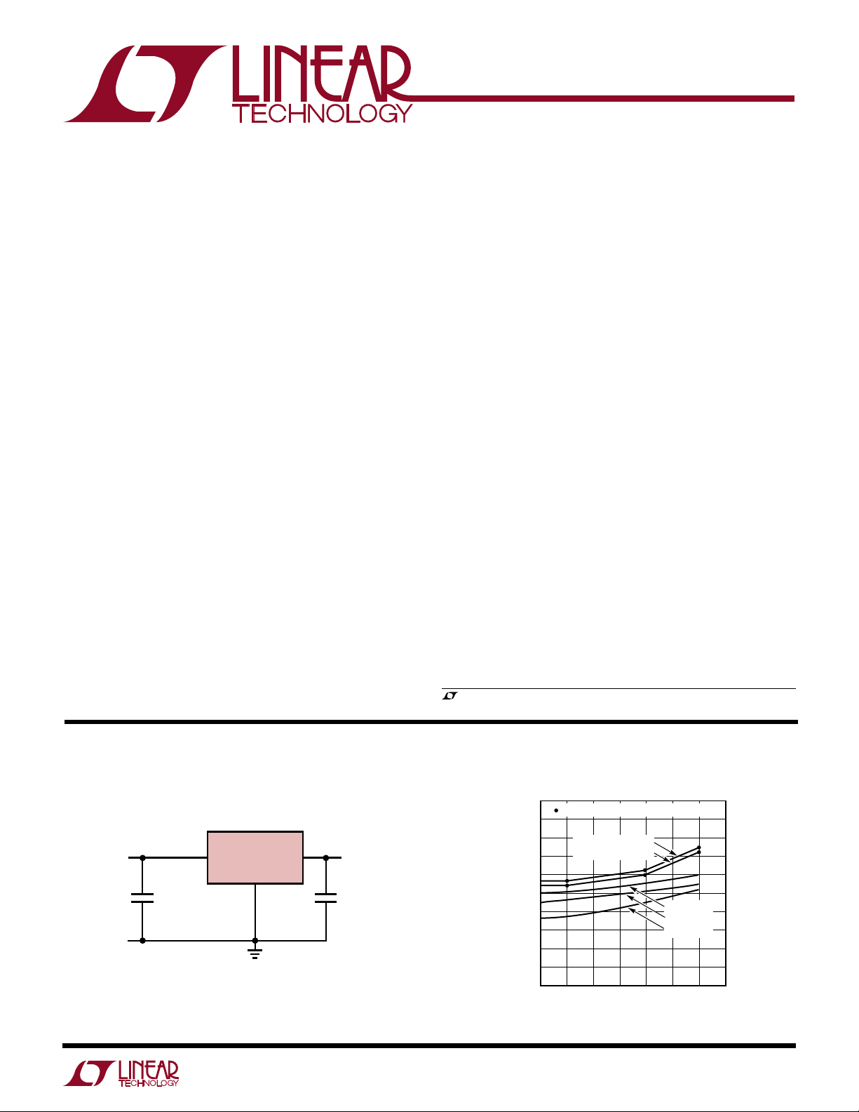
TYPICAL APPLICATION
5V to 3.3V Regulator
V
≥ 4.75V 3.3V AT 1.5A
IN
10µF*
TANTALUM
LT1086-3.3
IN OUT
GND
LT1086 • TA01
10µF
TANTALUM
The LT1086 is pin compatible with older 3-terminal adjustable regulators. A 10µF output capacitor is required on
these new devices; however, this is usually included in
most regulator designs.
A 2.85V output version is offered for SCSI-2 active termination. For surface mount applications see the LT1117-
2.85 data sheet. For high current or lower dropout requirements see the LT1123-2.85 data sheet.
Unlike PNP regulators, where up to 10% of the output
current is wasted as quiescent current, the LT1086 quiescent current flows into the load, increasing efficiency.
, LTC and LT are registered trademarks of Linear Technology Corporation.
LT1086 Dropout Voltage
2
INDICATES GUARANTEED TEST POINT
–55°C ≤ TJ ≤ 150°C
1
0°C ≤ T
≤ 125°C
J
= –55°C
T
J
= 25°C
T
J
= 150°C
T
J
*MAY BE OMITTED IF INPUT SUPPLY IS WELL
BYPASSED WITHIN 2" OF THE LT1086
MINIMUM INPUT/OUTPUT DIFFERENTIAL (V)
0
0
0.5
OUTPUT CURRENT (A)
1
1.5
LT1086 • TA02
1
LT1086 Series
WW
W
U
ABSOLUTE MAXIMUM RATINGS
Power Dissipation............................... Internally Limited
Input Voltage (Note 1) ............................................. 30V
Operating Input Voltage
Adjustable Devices ........................................... 25V
2.85V Devices .................................................. 18V
3.3V, 3.6V, and 5V Devices ............................... 20V
12V Devices ...................................................... 25V
Operating Junction Temperature Range
“C” Grades
Control Section ............................... 0°C to 125°C
Power Transistor............................. 0°C to 150°C
“I” Grades
Control Section .......................... –40°C to 125°C
Power Transistor........................ –40°C to 150°C
U
W
U
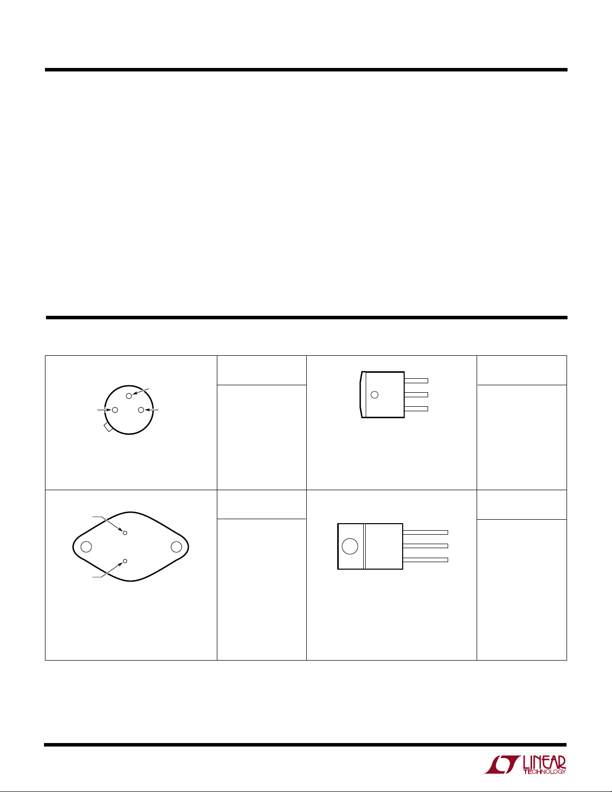
PACKAGE/ORDER INFORMATION
BOTTOM VIEW
V
IN
3-LEAD TO-39 METAL CAN
2
13
H PACKAGE
θJA = 150°C/W
ADJ
V
OUT
(CASE)
ORDER
PART NUMBER
LT1086CH
LT1086MH
“M” Grades
Control Section .......................... –55°C to 150°C
Power Transistor........................ –55°C to 200°C
Storage Temperature Range ................. – 65°C to 150°C
Lead Temperature (Soldering, 10 sec).................. 300°C
Note 1: Although the device’s maximum operating voltage is limited, (18V
for a 2.85V device, 20V for a 5V device, and 25V for adjustable and
12V devices) the devices are guaranteed to withstand transient input
voltages up to 30V. For input voltages greater than the maximum operating
input voltage some degradation of specifications will occur. For fixed
voltage devices operating at input/output voltage differentials greater than
15V, a minimum external load of 5mA is required to maintain regulation.
UUU
PRECONDITIONING
100% Thermal Shutdown Functional Test.
FRONT VIEW
3
TAB IS
OUTPUT
3-LEAD PLASTIC DD
θJA = 30°C/W**
** WITH PACKAGE SOLDERED TO 0.5IN2 COPPER AREA
OVER BACKSIDE GROUND PLANE OR INTERNAL POWER
PLANE. θ
DEPENDING ON MOUNTING TECHNIQUE.
CAN VARY FROM 20°C/W TO >40°C/W
JA
2
1
M PACKAGE
VIN
V
OUT
ADJ
(GND)*
ORDER
PART NUMBER
LT1086CM
LT1086CM-3.3
LT1086CM-3.6
LT1086IM
LT1086IM-3.3
LT1086IM-3.6
V
IN
ADJ (GND)*
2-LEAD TO-3 METAL CAN
*For fixed versions.
2
BOTTOM VIEW
2
1
K PACKAGE
θJA = 35°C/W
CASE
IS OUTPUT
ORDER
PART NUMBER
LT1086CK
LT1086CK-5
LT1086CK-12
LT1086IK
LT1086IK-5
LT1086IK-12
LT1086MK
LT1086MK-5
LT1086MK-12
TAB IS
OUTPUT
FRONT VIEW
3
2
1
T PACKAGE
3-LEAD PLASTIC TO-220
θJA = 50°C/W
VIN
V
OUT
ADJ
(GND)*
PART NUMBER
LT1086CT
LT1086CT-2.85
LT1086CT-3.3
LT1086IT
LT1086IT-5
LT1086IT-12
LT1086CT-3.6
LT1086CT-5
LT1086CT-12
ORDER
LT1086 Series
ELECTRICAL CHARACTERISTICS
PARAMETER CONDITIONS MIN TYP MAX UNITS
Reference Voltage LT1086, LT1086H I
(Note 2) 10mA ≤ I
Output Voltage LT1086-2.85 I
(Note 2) 0V ≤ I
LT1086-3.3 VIN = 5V, I
LT1086-3.6 VIN = 5V, I
LT1086-5 I
LT1086-12 I
Line Regulation LT1086, LT1086H I
LT1086-2.85 I
LT1086-3.3 4.5V ≤ VIN ≤ 18V, I
LT1086-3.6 4.75V ≤ VIN ≤ 18V, I
LT1086-5 I
LT1086-12 I
Load Regulation LT1086, LT1086H (VIN – V
LT1086-2.85 VIN = 5V, 0 ≤ I
LT1086-3.3 VIN = 5V, 0 ≤ I
LT1086-3.6 VIN = 5.25V, 0 ≤ I
LT1086-5 VIN = 8V, 0 ≤ I
LT1086-12 VIN = 15V, 0 ≤ I
Dropout Voltage LT1086/-2.85/-3.3/-3.6/-5/-12 ∆V
– V
OUT
)
(V
IN
LT1086H ∆V
= 10mA, TJ = 25°C, (VIN – V
OUT
OUT
4.75V ≤ V
5V ≤ V
4.75V ≤ V
= 4.75V, I
V
IN
OUT
0 ≤ I
OUT
0 ≤ I
LOAD
OUT
OUT
OUT
≤ 1.5A, (0.5A for LT1086H), 1.5V ≤ (VIN – V
OUT
= 0mA, TJ = 25°C, VIN = 5V 2.82 2.85 2.88 V
≤ 1.5A, 4.35V ≤ VIN ≤ 18V ● 2.79 2.85 2.91 V
OUT
= 0mA, TJ = 25°C 3.267 3.300 3.333 V
OUT
≤ 18V, 0V ≤ I
IN
= 0mA, TJ = 25°C 3.564 3.600 3.636 V
OUT
≤ 18V, 0 ≤ I
IN
≤ 18V, 0 ≤ I
IN
OUT
OUT
≤ 1.5A ● 3.500 3.672 V
OUT
OUT
= 1.5A, TJ ≥ 0°C 3.300 3.672 V
= 0mA, TJ = 25°C, VIN = 8V 4.950 5.000 5.050 V
≤ 1.5A, 6.5V ≤ VIN ≤ 20V ● 4.900 5.000 5.100 V
OUT
= 0mA, TJ = 25°C, VIN = 15V 11.880 12.000 12.120 V
≤ 1.5A, 13.5V ≤ VIN ≤ 25V ● 11.760 12.000 12.240 V
OUT
= 10mA, 1.5V ≤ (VIN – V
= 0mA, TJ = 25°C, 4.35V ≤ VIN ≤ 18V 0.3 6 mV
= 0mA, TJ = 25°C 0.5 10 mV
OUT
= 0mA, TJ = 25°C 0.5 10 mV
OUT
= 0mA, TJ = 25°C, 6.5V ≤ VIN ≤ 20V 0.5 10 mV
= 0mA, TJ = 25°C, 13.5V ≤ VIN ≤ 25V 1.0 25 mV
) = 3V, 10mA ≤ I
OUT
) = 3V 1.238 1.250 1.262 V
OUT
) ≤ 15V ● 1.225 1.250 1.270 V
OUT
≤ 1.5A ● 3.235 3.300 3.365 V
≤ 1A, TJ ≥ 0°C 3.500 3.672 V
) ≤ 15V, TJ = 25°C 0.015 0.2 %
OUT
≤ 1.5A, (0.5A for LT1086H)
OUT
● 0.035 0.2 %
● 0.6 6 mV
● 1.0 10 mV
● 1.0 10 mV
● 1.0 10 mV
● 2.0 25 mV
TJ = 25°C (Notes 1, 2) 0.1 0.3 %
● 0.2 0.4 %
≤ 1.5A, TJ = 25°C (Notes 1, 2) 3 12 mV
= 5V, 0 ≤ I
V
IN
= 1%, I
REF
OUT
≤ 1.5A, TJ = 25°C (Notes 1, 2) 3 15 mV
OUT
≤ 1.5A, TJ = 25°C (Notes 1, 2) 3 15 mV
OUT
≤ 1A, TJ = 25°C 2 15 mV
OUT
≤ 1.5A, TJ = 25°C (Notes 1, 2) 5 20 mV
OUT
≤ 1.5A, TJ = 25°C (Notes 1, 2) 12 36 mV
OUT
, ∆V
OUT
OUT
= 1%, I
REF
= 0.5A (Note 3) ● 0.95 1.25 V
= 1.5A (Note 3) ● 1.3 1.5 V
OUT
● 620 mV
● 725 mV
● 625 mV
● 425 mV
● 10 35 mV
● 24 72 mV
3
LT1086 Series
ELECTRICAL CHARACTERISTICS
PARAMETER CONDITIONS MIN TYP MAX UNITS
Current Limit LT1086/-2.85/-3.3/-3.6/-5/-12 (VIN – V
(V
IN
LT1086H (VIN – V
Minimum Load Current LT1086/LT1086H (VIN – V
(V
IN
– V
OUT
OUT
OUT
Quiescient Current LT1086-2.85 VIN ≤ 18V ● 510 mA
LT1086-3.3 V
LT1086-3.6 V
LT1086-5 V
≤ 18V ● 510 mA
IN
≤ 18V ● 510 mA
IN
≤ 20V ● 510 mA
IN
LT1086-12 VIN ≤ 25V ● 510 mA
Thermal Regulation TA = 25°C, 30ms pulse 0.008 0.04 %/W
Ripple Rejection f = 120Hz, C
LT1086, LT1086H C
LT1086-2.85 V
LT1086-3.3 V
LT1086-3.6 V
LT1086-5 V
= 25µF Tantalum, I
OUT
ADJ
= 6V ● 60 72 dB
IN
= 6.3V ● 60 72 dB
IN
= 6.6V ● 60 72 dB
IN
= 8V ● 60 68 dB
IN
= 25µF, (VIN – V
LT1083-12 VIN = 15V ● 54 60 dB
Adjust Pin Current LT1086, LT1086H TJ = 25°C55µA
Adjust Pin Current LT1086, LT1086H 10mA ≤ I
Change 1.5V ≤ (V
OUT
IN
Temperature Stability ● 0.5 %
Long Term Stability TA = 125°C, 1000 Hrs. 0.3 1 %
RMS Output Noise TA = 25°C, 10Hz = ≤ f ≤ 10kHz 0.003 %
OUT
)
(% of V
Thermal Resistance H Package: Control Circuitry/Power Transistor 15/20 °C/W
Junction-to-Case K Package: Control Circuitry/Power Transistor 1.7/4.0 °C/W
M Package: Control Circuitry/Power Transistor 1.5/4.0 °C/W
T Package: Control Circuitry/Power Transistor 1.5/4.0 °C/W
) = 5V ● 1.50 2.00 A
OUT
– V
) = 25V ● 0.05 0.15 A
OUT
) = 5V ● 0.50 0.700 A
) = 25V ● 0.02 0.075 A
) = 25V (Note 4) ● 510 mA
= 1.5A, (I
OUT
= 0.5A for LT1086H)
OUT
) = 3V ● 60 75 dB
OUT
●120 µA
≤ 1.5A, (0.5A for LT1086H)
– V
) ≤ 15V ● 0.2 5 µA
OUT
The ● denotes the specifications which apply over the full operating
temperature range.
Note 1: See thermal regulation specifications for changes in output voltage
due to heating effects. Line and load regulation are measured at a constant
junction temperature by low duty cycle pulse testing. Load regulation is
measured at the output lead ≈1/8" from the package.
Note 2: Line and load regulation are guaranteed up to the maximum power
dissipation of 15W (3W for the LT1086H). Power dissipation is determined
4
by the input/output differential and the output current. Guaranteed
maximum power dissipation will not be available over the full input/output
range. See Short-Circuit Current curve for available output current.
Note 3: Dropout voltage is specified over the full output current range of
the device. Test points and limits are shown on the Dropout Voltage curve.
Note 4: Minimum load current is defined as the minimum output current
required to maintain regulation. At 25V input/output differential the device
is guaranteed to regulate if the output current is greater than 10mA.
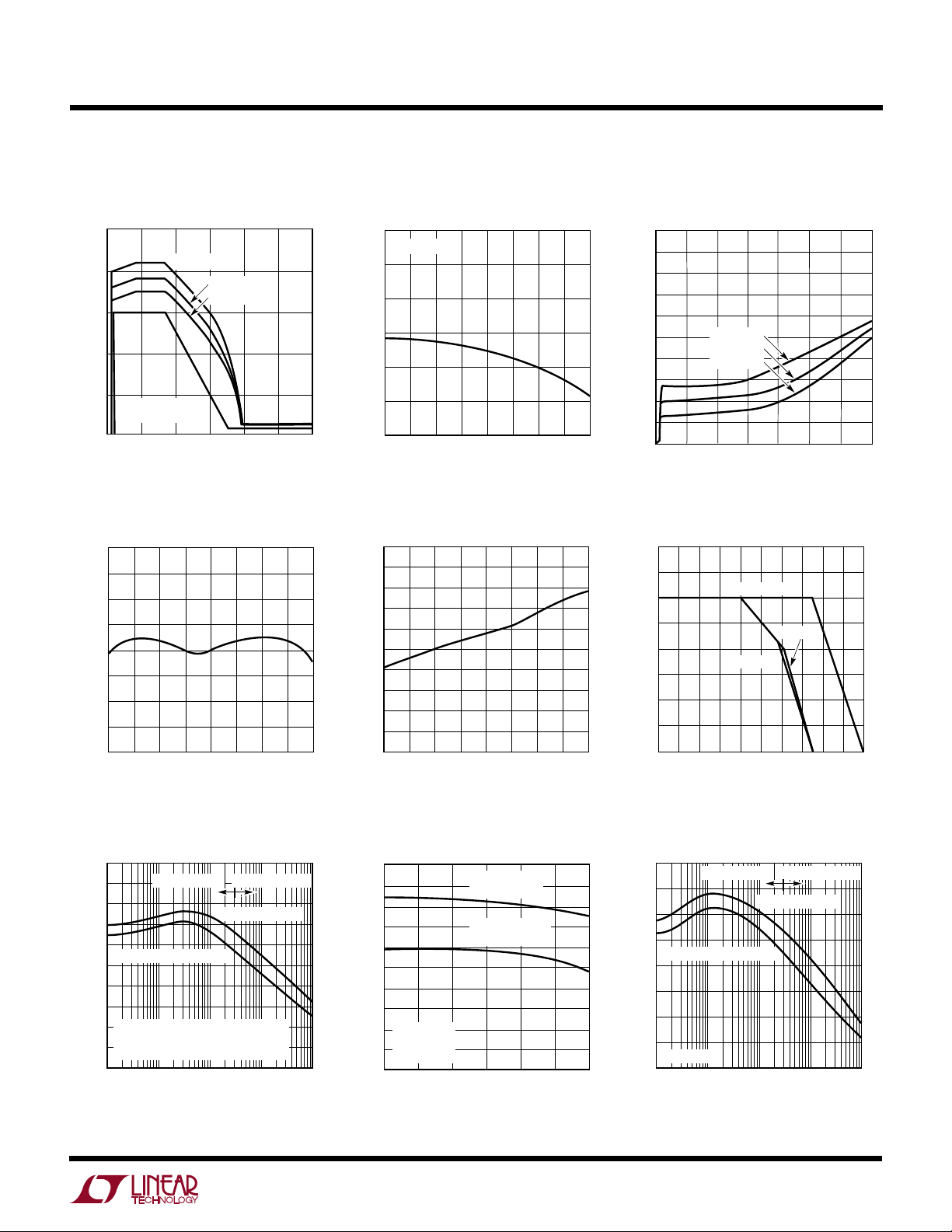
W
CASE TEMPERATURE (°C)
*AS LIMITED BY MAXIMUM JUNCTION TEMPERATURE
50
POWER (W)
15
20
130
LT1086 • TPC06
10
5
0
70
90
110
150
120
60
80
100
140
LT1086MK
LT1086CK
LT1086CT
INPUT/OUTPUT DIFFERENTIAL (V)
0
0
MINIMUM OPERATING CURRENT (mA)
1
3
4
5
10
7
10
20
25
LT1086 • TPC03
2
8
9
6
5
15
30
35
TJ = 150°C
T
J
= 25°C
T
J
= –55°C
U
TYPICAL PERFORMANCE CHARACTERISTICS
LT1086 Short-Circuit Current
2.5
2.0
1.5
1.0
SHORT-CIRCUIT CURRENT (A)
0.5
0
0
TJ = 150°C
GUARANTEED
OUTPUT CURRENT
10 15 20
5
INPUT/OUTPUT DIFFERENTIAL (V)
Temperature Stability
2
1
0
–1
OUTPUT VOLTAGE CHANGE (%)
–2
–25
–50
0
50
25
TEMPERATURE (°C)
TJ = 25°C
= –55°C
T
J
75
25 30
LT1086 • TPC01
100
LT1086 • TPC04
125
150
0.10
∆I = 1.5A
0.05
0
–0.05
–0.10
–0.15
OUTPUT VOLTAGE DEVIATION (%)
–0.20
–50
050
–25 25
TEMPERATURE (°C)
Adjust Pin Current
100
90
80
70
60
50
40
30
ADJUST PIN CURRENT (µA)
20
10
0
–50
–25 25
0
50
TEMPERATURE (°C)
100
75
LT1086 • TPC02
125
100
75
LT1086 • TPC05
125
LT1086 Series
Minimum Operating Current
(Adjustable Device)LT1086 Load Regulation
150
LT1086 Maximum Power
Dissipation*
150
LT1086 Ripple Rejection
100
V
≤ 3V
90
80
70
60
50
40
30
RIPPLE REJECTION (dB)
20
10
0
10 1k 10k 100k
RIPPLE
(VIN – V
OUT
C
= 200µF AT FREQUENCIES < 60Hz
ADJ
= 25µF AT FREQUENCIES > 60Hz
C
ADJ
= 1.5A
I
OUT
100
P-P
(VIN – V
) ≥ V
DROPOUT
FREQUENCY (Hz)
V
RIPPLE
OUT
≤ 0.5V
) ≥ 3V
LT1086 • TPC07
P-P
LT1086 Ripple Rejection
vs Current
100
90
80
70
60
50
40
30
RIPPLE REJECTION (dB)
V
20
10
= 5V
OUT
= 25µF
C
ADJ
= 25µF
C
OUT
0
0
0.25
fR = 120Hz
V
fR = 20kHz
V
0.5
OUTPUT CURRENT (A)
≤ 3V
RIPPLE
≤ 0.5V
RIPPLE
0.75 1.0
P-P
P-P
1.25
LT1086 • TPC08
RIPPLE REJECTION (dB)
1.5
LT1086-5 Ripple Rejection
80
70
60
50
40
30
20
10
0
10 1k 10k 100k
(V
I
OUT
– V
IN
= 1.5A
V
≤ 3V
RIPPLE
) ≥ V
OUT
DROPOUT
100
FREQUENCY (Hz)
P-P
(VIN – V
V
RIPPLE
OUT
≤ 0.5V
) ≥ 3V
LT1086 • TPC09
P-P
5