

Linear Technology LT1076CT7, LT1076CK, LT1076IT, LT1076IR, LT1076 Datasheet
...
LT1074/LT1076
Step-Down Switching
Regulator
FEATURES
■
5A Onboard Switch (LT1074)
■
100kHz Switching Frequency
■
Greatly Improved Dynamic Behavior
■
Available in Low Cost 5 and 7-Lead Packages
■
Only 8.5mA Quiescent Current
■
Programmable Current Limit
■
Operates Up to 60V Input
■
Micropower Shutdown Mode
U
APPLICATIO S
■
Buck Converter with Output Voltage Range of 2.5V
to 50V
■
Tapped-Inductor Buck Converter with 10A Output
at 5V
■
Positive-to-Negative Converter
■
Negative Boost Converter
■
Multiple Output Buck Converter
U
DESCRIPTIO
The LT®1074 is a 5A (LT1076 is rated at 2A) monolithic
bipolar switching regulator which requires only a few
external parts for normal operation. The power switch, all
oscillator and control circuitry, and all current limit components, are included on the chip. The topology is a classic
positive “buck” configuration but several design innovations allow this device to be used as a positive-to-negative
converter, a negative boost converter, and as a flyback
converter. The switch output is specified to swing 40V
below ground, allowing the LT1074 to drive a tappedinductor in the buck mode with output currents up to 10A.
The LT1074 uses a true analog multiplier in the feedback
loop. This makes the device respond nearly instantaneously to input voltage fluctuations and makes loop gain
independent of input voltage. As a result, dynamic behavior of the regulator is significantly improved over previous
designs.
On-chip pulse by pulse current limiting makes the LT1074
nearly bust-proof for output overloads or shorts. The input
voltage range as a buck converter is 8V to 60V, but a selfboot feature allows input voltages as low as 5V in the
inverting and boost configurations.
The LT1074 is available in low cost TO-220 or TO-3
packages with frequency pre-set at 100kHz and current
limit at 6.5A (LT1076 = 2.6A). A 7-pin TO-220 package is
also available which allows current limit to be adjusted
down to zero. In addition, full micropower shutdown can
be programmed. See Application Note 44 for design
details.
A fixed 5V output, 2A version is also available. See LT1076-5.
, LTC and LT are registered trademarks of Linear Technology Corporation.
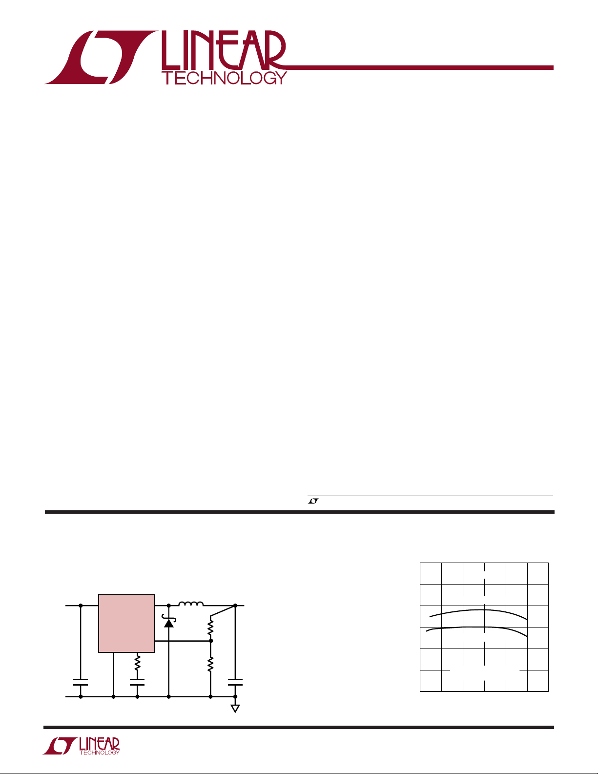
TYPICAL APPLICATIO
Basic Positive Buck Converter
50
µH (LT1074)
100
µH (LT1076)
MBR745*
µF
10V TO 40V
LT1074
V
SW
FB
V
C
R3
2.7k
C2
0.01
V
IN
GND
+
†
C3
200µF
L1**
U
R1
2.8k
1%
R2
2.21k
1%
Buck Converter Efficiency
100
5V
USE MBR340 FOR LT1076
*
5A
COILTRONICS #50-2-52 (LT1074)
**
PULSE ENGINEERING, INC.
HURRICANE #HL-AK147QQ (LT1074)
+
25V
†
C1
RIPPLE CURRENT RATING ≥ I
500
µF
#100-1-52 (LT1076)
#PE-92114 (LT1074)
#PE-92102 (LT1076)
#HL-AG210LL (LT1076)
/2
OUT
LT1074•TA01
90
80
EFFICIENCY (%)
70
60
50
0
1234
OUTPUT LOAD CURRENT (A)
LT1074
V = 12V, V = 20V
OUT IN
V = 5V, V = 15V
OUT IN
L = 50µH TYPE 52 CORE
DIODE = MBR735
5
LT1074•TPC27
6
1
LT1074/LT1076
WW
W
ABSOLUTE AXI U RATI GS
U
(Note 1)
Input Voltage
LT1074/ LT1076 .................................................. 45V
LT1074HV/LT1076HV ......................................... 64V
Switch Voltage with Respect to Input Voltage
LT1074/ LT1076 .................................................. 64V
LT1074HV/LT1076HV ......................................... 75V
Switch Voltage with Respect to Ground Pin (V
Negative)
SW
LT1074/LT1076 (Note 7) ..................................... 35V
LT1074HV/LT1076HV (Note 7) ........................... 45V
Feedback Pin Voltage..................................... –2V, +10V
Shutdown Pin Voltage (Not to Exceed VIN).............. 40V
UUW
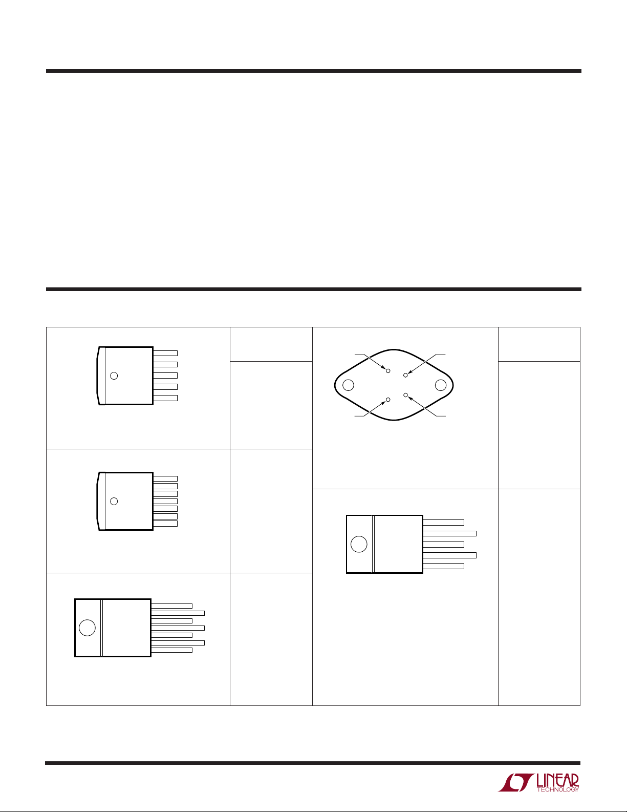
PACKAGE/ORDER I FOR ATIO
ORDER PART
LT1076CQ
LT1076IQ
LT1076CR
LT1076IR
LT1076HVCR
LT1076HVIR
LT1074CT7
LT1074HVCT7
C
LT1074IT7
LT1074HVIT7
LT1076CT7
SW
IN
LT1076HVCT7
NUMBER
TAB IS
GND
FRONT VIEW
TAB IS
GND
Q PACKAGE
5-LEAD PLASTIC DD
LT1076: θJC = 4°C, θJA = 30°C/W
FRONT VIEW
TAB IS
GND
R PACKAGE
7-LEAD PLASTIC DD
LT1076: θ
= 4°C, θJA = 30°C/W
JC
FRONT VIEW
T7 PACKAGE
7-LEAD PLASTIC TO-220
5
4
3
2
1
7
6
5
4
3
2
1
7
6
5
4
3
2
1
V
IN
V
SW
GND
V
C
FB/SENSE
SHDN
V
C
FB/SENSE
GND
I
LIM
V
SW
V
IN
SHDN
V
FB
GND
I
LIM
V
V
I
Pin Voltage (Forced) ............................................ 5.5V
LIM
Maximum Operating Ambient Temperature Range
Commercial ................................................. 0°C to 70°C
Industrial ................................................ –40°C to 85°C
Military ................................................. –55°C to 125°C
Maximum Operating Junction Temperature Range
Commercial ............................................... 0°C to 125°C
Industrial .............................................. –40°C to 125°C
Military ................................................. –55°C to 150°C
Maximum Storage Temperature ............... –65°C to 150°C
Lead Temperature (Soldering, 10 sec)......................300°C
ORDER PART
LT1074CK
LT1074HVCK
LT1074MK
LT1074HVMK
LT1076CK
LT1076HVCK
LT1076MK
LT1076HVMK
LT1074CT
LT1074HVCT
V
IN
V
SW
LT1074IT
GND
LT1074HVIT
V
C
LT1076CT
FB
LT1076HVCT
LT1076IT
LT1076HVIT
NUMBER
TAB IS
GND
BOTTOM VIEW
V
C
1
2
3
4
FB
K PACKAGE
4-LEAD TO-3 METAL CAN
LT1074: θ
LT1074: θ
= 2.5°C, θJA = 35°C/W
JC
LT1076: θ
LT1076: θ
= 4°C, θJA = 35°C/W
JC
FRONT VIEW
5
4
3
2
1
T PACKAGE
5-LEAD PLASTIC TO-220
LEADS ARE FORMED STANDARD FOR
STRAIGHT LEADS, ORDER FLOW 06
= 2.5°C, θJA = 50°C/W
JC
= 4°C, θJA = 50°C/W
JC
V
IN
CASE
IS GND
V
SW
LT1074: θ
LT1076: θ
= 2.5°C, θJA = 50°C/W
JC
= 4°C, θJA = 50°C/W
JC
*Assumes package is soldered to 0.5 IN2 of 1 oz. copper over internal ground plane or over back side plane.
2
LT1074/LT1076
ELECTRICAL CHARACTERISTICS
The ● denotes the specifications which apply over the full operating
temperature range, otherwise specifications are at TA = 25°C. Tj = 25°C, VIN = 25V, unless otherwise noted.
PARAMETER CONDITIONS MIN TYP MAX UNITS
Switch “On” Voltage (Note 2) LT1074 I
LT1076 I
Switch “Off” Leakage LT1074 V
LT1076 V
Supply Current (Note 3) V
= 2.5V, V
FB
40V < V
V
SHUT
Minimum Supply Voltage Normal Mode ● 7.3 8 V
Startup Mode (Note 4)
Switch Current Limit (Note 5) LT1074 I
LT1076 I
Maximum Duty Cycle ● 85 90 %
Switching Frequency 90 100 110 kHz
≤ 125°C ● 85 120 kHz
T
j
T
> 125°C ● 85 125 kHz
j
= 0V through 2kΩ (Note 5) 20 kHz
V
FB
Switching Frequency Line Regulation 8V ≤ V
Error Amplifier Voltage Gain (Note 7) 1V ≤ VC ≤ 4V 2000 V/V
Error Amplifier Transconductance 3700 5000 8000 µmho
Error Amplifier Source and Sink Current Source (V
Sink (V
Feedback Pin Bias Current V
FB
= V
Reference Voltage VC = 2V ● 2.155 2.21 2.265 V
Reference Voltage Tolerance V
(Nominal) = 2.21V ±0.5 ±1.5 %
REF
All Conditions of Input Voltage, Output
Voltage, Temperature and Load Current
Reference Voltage Line Regulation 8V ≤ VIN ≤ V
VC Voltage at 0% Duty Cycle 1.5 V
Over Temperature
Multiplier Reference Voltage 24 V
Shutdown Pin Current V
= 5V ● 51020 µA
SH
≤ V
V
SH
Shutdown Thresholds Switch Duty Cycle = 0 ● 2.2 2.45 2.7 V
Fully Shut Down
Thermal Resistance Junction to Case LT1074 2.5 °C/W
LT1076 4.0 °C/W
= 1A, Tj ≥ 0°C 1.85 V
SW
= 1A, Tj < 0°C 2.1 V
I
SW
I
= 5A, Tj ≥ 0°C 2.3 V
SW
= 5A, Tj < 0°C 2.5 V
I
SW
= 0.5A ● 1.2 V
SW
= 2A ● 1.7 V
I
SW
≤ 25V, V
IN
= V
V
IN
MAX, VSW
= 25V, V
IN
V
= V
IN
MAX, VSW
≤ 40V ● 8.5 11 mA
IN
< 60V ● 912 mA
IN
= 0 5 300 µA
SW
= 0 (Note 8) 10 500 µA
= 0 150 µA
SW
= 0 (Note 8) 250 µA
= 0.1V (Device Shutdown) (Note 9) ● 140 300 µA
● 3.5 4.8 V
Open ● 5.5 6.5 8.5 A
LIM
= 10k (Note 6) 4.5 A
R
LIM
R
= 7k (Note 6) 3 A
LIM
Open ● 2 2.6 3.2 A
LIM
R
= 10k (Note 6) 1.8 A
LIM
R
= 7k (Note 6) 1.2 A
LIM
≤ V
IN
FB
REF
(Note 8) ● 0.03 0.1 %/V
MAX
= 2V) 100 140 225 µA
FB
= 2.5V) 0.7 1 1.6 mA
● 0.5 2 µA
● ±1 ±2.5 %
(Note 8) ● 0.005 0.02 %/V
MAX
● – 4 mV/°C
THRESHOLD
(≅2.5V) ● 50 µA
● 0.1 0.3 0.5 V
3
LT1074/LT1076
ELECTRICAL CHARACTERISTICS
Note 1: Absolute Maximum Ratings are those values beyond which the life
of a device may be impaired.
Note 2: To calculate maximum switch “on” voltage at currents between
low and high conditions, a linear interpolation may be used.
Note 3: A feedback pin voltage (V
) of 2.5V forces the VC pin to its low
FB
clamp level and the switch duty cycle to zero. This approximates the zero
load condition where duty cycle approaches zero.
Note 4: Total voltage from V
pin to ground pin must be ≥ 8V after start-
IN
up for proper regulation.
W
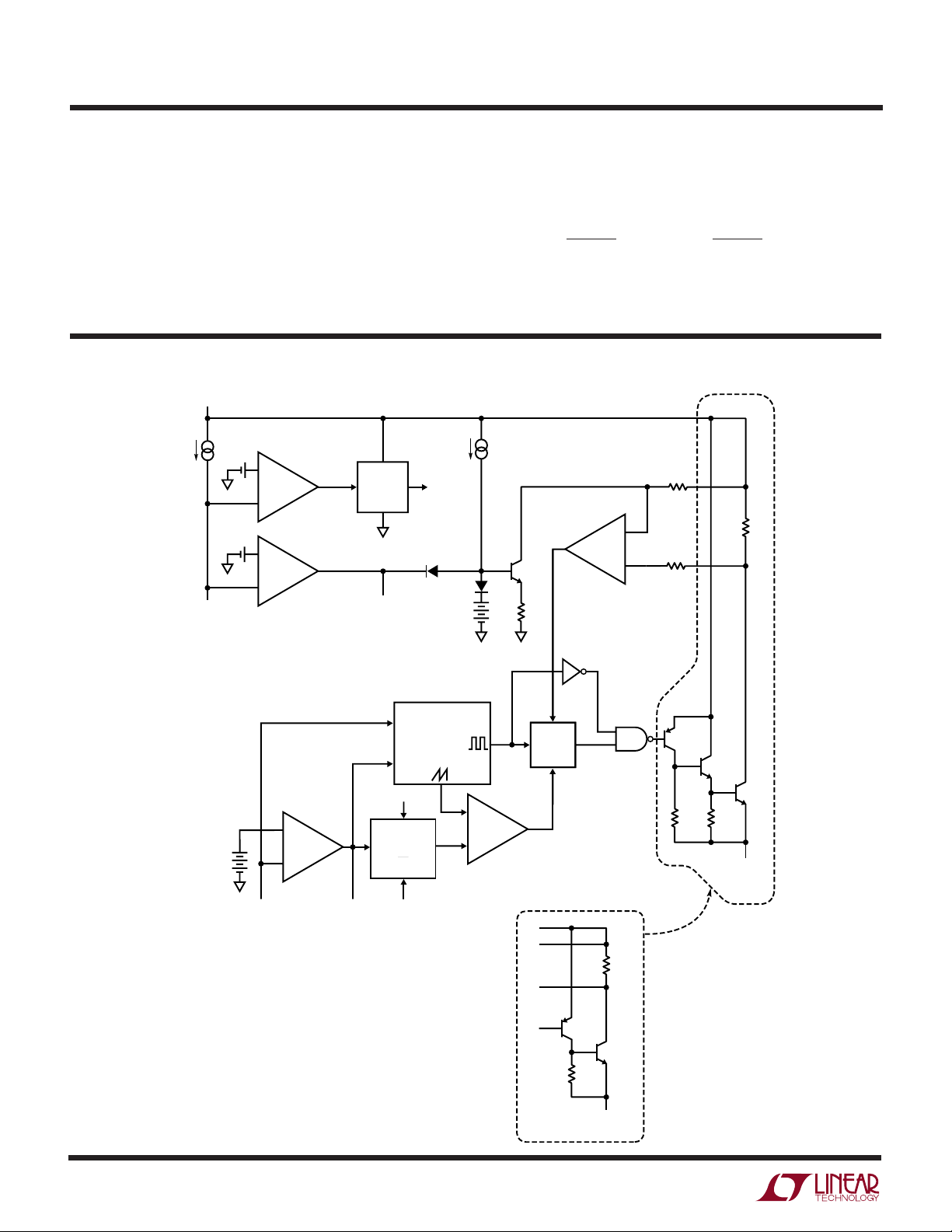
BLOCK DIAGRA
INPUT SUPPLY
10 Aµ
SHUTDOWN*
0.3V
2.35V
+
-POWER
µ
SHUTDOWN
–
+
–
CURRENT
LIMIT
SHUTDOWN
6V
REGULATOR
AND BIAS
I *
LIM
320 Aµ
6V TO ALL
CIRCUITRY
Note 5: Switch frequency is internally scaled down when the feedback pin
voltage is less than 1.3V to avoid extremely short switch on times. During
testing, V
Note 6: I
is adjusted to give a minimum switch on time of 1µs.
FB
R
LIM
2k
– 1k
LIM
≈ (LT1074), I
R
– 1k
LIM
≈ (LT1076).
LIM
5.5k
Note 7: Switch to input voltage limitation must also be observed.
Note 8: V
= 40V for the LT1074/76 and 60V for the LT1074HV/76HV.
MAX
Note 9: Does not include switch leakage.
LT1074
500
Ω
CURRENT
4.5V
10k
LIMIT
COMP
+
C2
–
250
Ω
0.04
+
A1
ERROR
2.21V
*AVAILABLE ON PACKAGES WITH PIN
COUNTS GREATER THAN 5.
AMP
–
FB V
X
C
FREQ SHIFT
100kHz
OSCILLATOR
SYNC
V
IN
Z
ANALOG
MULTIPLIER
XY
Z
Y
24V (EQUIVALENT)
3V(p-p)
+
–
C1
PULSE WIDTH
COMPARATOR
S
R
R/S
LATCH
R
Q
LT1076
100
Ω
SWITCH
OUTPUT (V )
G1
Ω
15
400
Ω
SWITCH
OUTPUT
(V )
SW
0.1
Ω
SW
LT1074 • BD01
4

LT1074/LT1076
W
BLOCK DIAGRA
A switch cycle in the LT1074 is initiated by the oscillator
setting the R/S latch. The pulse that sets the latch also
locks out the switch via gate G1. The effective width of this
pulse is approximately 700ns, which sets the maximum
switch duty cycle to approximately 93% at 100kHz switching frequency. The switch is turned off by comparator C1,
which resets the latch. C1 has a sawtooth waveform as one
input and the output of an analog multiplier as the other
input. The multiplier output is the product of an internal
reference voltage, and the output of the error amplifier, A1,
divided by the regulator input voltage. In standard buck
regulators, this means that the output voltage of A1
required to keep a constant regulated output is independent of regulator input voltage. This greatly improves line
transient response, and makes loop gain independent of
input voltage. The error amplifier is a transconductance
type with a GM at null of approximately 5000µmho. Slew
current going positive is 140µA, while negative slew
current is about 1.1mA. This asymmetry helps prevent
overshoot on start-up. Overall loop frequency compensation is accomplished with a series RC network from VC to
ground.
Switch current is continuously monitored by C2, which
resets the R/S latch to turn the switch off if an overcurrent
condition occurs. The time required for detection and
switch turn off is approximately 600ns. So minimum
switch “on” time in current limit is 600ns. Under dead
shorted output conditions, switch duty cycle may have to
be as low as 2% to maintain control of output current. This
would require switch on time of 200ns at 100kHz switching frequency, so frequency is reduced at very low output
DESCRIPTIO
U
voltages by feeding the FB signal into the oscillator and
creating a linear frequency downshift when the FB signal
drops below 1.3V. Current trip level is set by the voltage on
the I
source. When this pin is left open, it self-clamps at about
4.5V and sets current limit at 6.5A for the LT1074 and 2.6A
for the LT1076. In the 7-pin package an external resistor
can be connected from the I
current limit. A capacitor in parallel with this resistor will
soft-start the current limit. A slight offset in C2 guarantees
that when the I
C2 output will stay high and force switch duty cycle to zero.
The “Shutdown” pin is used to force switch duty cycle to
zero by pulling the I
the regulator. Threshold for the former is approximately
2.35V, and for complete shutdown, approximately 0.3V.
Total supply current in shutdown is about 150µA. A 10µA
pull-up current forces the shutdown pin high when left
open. A capacitor can be used to generate delayed startup. A resistor divider will program “undervoltage lockout”
if the divider voltage is set at 2.35V when the input is at the
desired trip point.
The switch used in the LT1074 is a Darlington NPN (single
NPN for LT1076) driven by a saturated PNP. Special
patented circuitry is used to drive the PNP on and off very
quickly even from the saturation state. This particular
switch arrangement has no “isolation tubs” connected to
the switch output, which can therefore swing to 40V below
ground.
pin which is driven by an internal 320µA current
LIM
pin to ground to set a lower
LIM
pin is pulled to within 200mV of ground,
LIM
pin low, or to completely shut down
LIM
5
 Loading...