

LT1074/LT1076
Step-Down Switching
Regulator
FEATURES
■
5A Onboard Switch (LT1074)
■
100kHz Switching Frequency
■
Greatly Improved Dynamic Behavior
■
Available in Low Cost 5 and 7-Lead Packages
■
Only 8.5mA Quiescent Current
■
Programmable Current Limit
■
Operates Up to 60V Input
■
Micropower Shutdown Mode
U
APPLICATIO S
■
Buck Converter with Output Voltage Range of 2.5V
to 50V
■
Tapped-Inductor Buck Converter with 10A Output
at 5V
■
Positive-to-Negative Converter
■
Negative Boost Converter
■
Multiple Output Buck Converter
U
DESCRIPTIO
The LT®1074 is a 5A (LT1076 is rated at 2A) monolithic
bipolar switching regulator which requires only a few
external parts for normal operation. The power switch, all
oscillator and control circuitry, and all current limit components, are included on the chip. The topology is a classic
positive “buck” configuration but several design innovations allow this device to be used as a positive-to-negative
converter, a negative boost converter, and as a flyback
converter. The switch output is specified to swing 40V
below ground, allowing the LT1074 to drive a tappedinductor in the buck mode with output currents up to 10A.
The LT1074 uses a true analog multiplier in the feedback
loop. This makes the device respond nearly instantaneously to input voltage fluctuations and makes loop gain
independent of input voltage. As a result, dynamic behavior of the regulator is significantly improved over previous
designs.
On-chip pulse by pulse current limiting makes the LT1074
nearly bust-proof for output overloads or shorts. The input
voltage range as a buck converter is 8V to 60V, but a selfboot feature allows input voltages as low as 5V in the
inverting and boost configurations.
The LT1074 is available in low cost TO-220 or TO-3
packages with frequency pre-set at 100kHz and current
limit at 6.5A (LT1076 = 2.6A). A 7-pin TO-220 package is
also available which allows current limit to be adjusted
down to zero. In addition, full micropower shutdown can
be programmed. See Application Note 44 for design
details.
A fixed 5V output, 2A version is also available. See LT1076-5.
, LTC and LT are registered trademarks of Linear Technology Corporation.
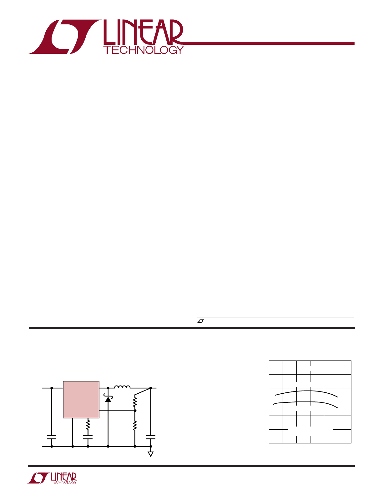
TYPICAL APPLICATIO
Basic Positive Buck Converter
50
µH (LT1074)
100
µH (LT1076)
MBR745*
µF
10V TO 40V
LT1074
V
SW
FB
V
C
R3
2.7k
C2
0.01
V
IN
GND
+
†
C3
200µF
L1**
U
R1
2.8k
1%
R2
2.21k
1%
Buck Converter Efficiency
100
5V
USE MBR340 FOR LT1076
*
5A
COILTRONICS #50-2-52 (LT1074)
**
PULSE ENGINEERING, INC.
HURRICANE #HL-AK147QQ (LT1074)
+
25V
†
C1
RIPPLE CURRENT RATING ≥ I
500
µF
#100-1-52 (LT1076)
#PE-92114 (LT1074)
#PE-92102 (LT1076)
#HL-AG210LL (LT1076)
/2
OUT
LT1074•TA01
90
80
EFFICIENCY (%)
70
60
50
0
1234
OUTPUT LOAD CURRENT (A)
LT1074
V = 12V, V = 20V
OUT IN
V = 5V, V = 15V
OUT IN
L = 50µH TYPE 52 CORE
DIODE = MBR735
5
LT1074•TPC27
6
1
LT1074/LT1076
WW
W
ABSOLUTE AXI U RATI GS
U
(Note 1)
Input Voltage
LT1074/ LT1076 .................................................. 45V
LT1074HV/LT1076HV ......................................... 64V
Switch Voltage with Respect to Input Voltage
LT1074/ LT1076 .................................................. 64V
LT1074HV/LT1076HV ......................................... 75V
Switch Voltage with Respect to Ground Pin (V
Negative)
SW
LT1074/LT1076 (Note 7) ..................................... 35V
LT1074HV/LT1076HV (Note 7) ........................... 45V
Feedback Pin Voltage..................................... –2V, +10V
Shutdown Pin Voltage (Not to Exceed VIN).............. 40V
UUW
PACKAGE/ORDER I FOR ATIO
ORDER PART
LT1076CQ
LT1076IQ
LT1076CR
LT1076IR
LT1076HVCR
LT1076HVIR
LT1074CT7
LT1074HVCT7
C
LT1074IT7
LT1074HVIT7
LT1076CT7
SW
IN
LT1076HVCT7
NUMBER
TAB IS
GND
FRONT VIEW
TAB IS
GND
Q PACKAGE
5-LEAD PLASTIC DD
LT1076: θJC = 4°C, θJA = 30°C/W
FRONT VIEW
TAB IS
GND
R PACKAGE
7-LEAD PLASTIC DD
LT1076: θ
= 4°C, θJA = 30°C/W
JC
FRONT VIEW
T7 PACKAGE
7-LEAD PLASTIC TO-220
5
4
3
2
1
7
6
5
4
3
2
1
7
6
5
4
3
2
1
V
IN
V
SW
GND
V
C
FB/SENSE
SHDN
V
C
FB/SENSE
GND
I
LIM
V
SW
V
IN
SHDN
V
FB
GND
I
LIM
V
V
I
Pin Voltage (Forced) ............................................ 5.5V
LIM
Maximum Operating Ambient Temperature Range
Commercial ................................................. 0°C to 70°C
Industrial ................................................ –40°C to 85°C
Military ................................................. –55°C to 125°C
Maximum Operating Junction Temperature Range
Commercial ............................................... 0°C to 125°C
Industrial .............................................. –40°C to 125°C
Military ................................................. –55°C to 150°C
Maximum Storage Temperature ............... –65°C to 150°C
Lead Temperature (Soldering, 10 sec)......................300°C
ORDER PART
LT1074CK
LT1074HVCK
LT1074MK
LT1074HVMK
LT1076CK
LT1076HVCK
LT1076MK
LT1076HVMK
LT1074CT
LT1074HVCT
V
IN
V
SW
LT1074IT
GND
LT1074HVIT
V
C
LT1076CT
FB
LT1076HVCT
LT1076IT
LT1076HVIT
NUMBER
TAB IS
GND
BOTTOM VIEW
V
C
1
2
3
4
FB
K PACKAGE
4-LEAD TO-3 METAL CAN
LT1074: θ
LT1074: θ
= 2.5°C, θJA = 35°C/W
JC
LT1076: θ
LT1076: θ
= 4°C, θJA = 35°C/W
JC
FRONT VIEW
5
4
3
2
1
T PACKAGE
5-LEAD PLASTIC TO-220
LEADS ARE FORMED STANDARD FOR
STRAIGHT LEADS, ORDER FLOW 06
= 2.5°C, θJA = 50°C/W
JC
= 4°C, θJA = 50°C/W
JC
V
IN
CASE
IS GND
V
SW
LT1074: θ
LT1076: θ
= 2.5°C, θJA = 50°C/W
JC
= 4°C, θJA = 50°C/W
JC
*Assumes package is soldered to 0.5 IN2 of 1 oz. copper over internal ground plane or over back side plane.
2
LT1074/LT1076
ELECTRICAL CHARACTERISTICS
The ● denotes the specifications which apply over the full operating
temperature range, otherwise specifications are at TA = 25°C. Tj = 25°C, VIN = 25V, unless otherwise noted.
PARAMETER CONDITIONS MIN TYP MAX UNITS
Switch “On” Voltage (Note 2) LT1074 I
LT1076 I
Switch “Off” Leakage LT1074 V
LT1076 V
Supply Current (Note 3) V
= 2.5V, V
FB
40V < V
V
SHUT
Minimum Supply Voltage Normal Mode ● 7.3 8 V
Startup Mode (Note 4)
Switch Current Limit (Note 5) LT1074 I
LT1076 I
Maximum Duty Cycle ● 85 90 %
Switching Frequency 90 100 110 kHz
≤ 125°C ● 85 120 kHz
T
j
T
> 125°C ● 85 125 kHz
j
= 0V through 2kΩ (Note 5) 20 kHz
V
FB
Switching Frequency Line Regulation 8V ≤ V
Error Amplifier Voltage Gain (Note 7) 1V ≤ VC ≤ 4V 2000 V/V
Error Amplifier Transconductance 3700 5000 8000 µmho
Error Amplifier Source and Sink Current Source (V
Sink (V
Feedback Pin Bias Current V
FB
= V
Reference Voltage VC = 2V ● 2.155 2.21 2.265 V
Reference Voltage Tolerance V
(Nominal) = 2.21V ±0.5 ±1.5 %
REF
All Conditions of Input Voltage, Output
Voltage, Temperature and Load Current
Reference Voltage Line Regulation 8V ≤ VIN ≤ V
VC Voltage at 0% Duty Cycle 1.5 V
Over Temperature
Multiplier Reference Voltage 24 V
Shutdown Pin Current V
= 5V ● 51020 µA
SH
≤ V
V
SH
Shutdown Thresholds Switch Duty Cycle = 0 ● 2.2 2.45 2.7 V
Fully Shut Down
Thermal Resistance Junction to Case LT1074 2.5 °C/W
LT1076 4.0 °C/W
= 1A, Tj ≥ 0°C 1.85 V
SW
= 1A, Tj < 0°C 2.1 V
I
SW
I
= 5A, Tj ≥ 0°C 2.3 V
SW
= 5A, Tj < 0°C 2.5 V
I
SW
= 0.5A ● 1.2 V
SW
= 2A ● 1.7 V
I
SW
≤ 25V, V
IN
= V
V
IN
MAX, VSW
= 25V, V
IN
V
= V
IN
MAX, VSW
≤ 40V ● 8.5 11 mA
IN
< 60V ● 912 mA
IN
= 0 5 300 µA
SW
= 0 (Note 8) 10 500 µA
= 0 150 µA
SW
= 0 (Note 8) 250 µA
= 0.1V (Device Shutdown) (Note 9) ● 140 300 µA
● 3.5 4.8 V
Open ● 5.5 6.5 8.5 A
LIM
= 10k (Note 6) 4.5 A
R
LIM
R
= 7k (Note 6) 3 A
LIM
Open ● 2 2.6 3.2 A
LIM
R
= 10k (Note 6) 1.8 A
LIM
R
= 7k (Note 6) 1.2 A
LIM
≤ V
IN
FB
REF
(Note 8) ● 0.03 0.1 %/V
MAX
= 2V) 100 140 225 µA
FB
= 2.5V) 0.7 1 1.6 mA
● 0.5 2 µA
● ±1 ±2.5 %
(Note 8) ● 0.005 0.02 %/V
MAX
● – 4 mV/°C
THRESHOLD
(≅2.5V) ● 50 µA
● 0.1 0.3 0.5 V
3
LT1074/LT1076
ELECTRICAL CHARACTERISTICS
Note 1: Absolute Maximum Ratings are those values beyond which the life
of a device may be impaired.
Note 2: To calculate maximum switch “on” voltage at currents between
low and high conditions, a linear interpolation may be used.
Note 3: A feedback pin voltage (V
) of 2.5V forces the VC pin to its low
FB
clamp level and the switch duty cycle to zero. This approximates the zero
load condition where duty cycle approaches zero.
Note 4: Total voltage from V
pin to ground pin must be ≥ 8V after start-
IN
up for proper regulation.
W
BLOCK DIAGRA
INPUT SUPPLY
10 Aµ
SHUTDOWN*
0.3V
2.35V
+
-POWER
µ
SHUTDOWN
–
+
–
CURRENT
LIMIT
SHUTDOWN
6V
REGULATOR
AND BIAS
I *
LIM
320 Aµ
6V TO ALL
CIRCUITRY
Note 5: Switch frequency is internally scaled down when the feedback pin
voltage is less than 1.3V to avoid extremely short switch on times. During
testing, V
Note 6: I
is adjusted to give a minimum switch on time of 1µs.
FB
R
LIM
2k
– 1k
LIM
≈ (LT1074), I
R
– 1k
LIM
≈ (LT1076).
LIM
5.5k
Note 7: Switch to input voltage limitation must also be observed.
Note 8: V
= 40V for the LT1074/76 and 60V for the LT1074HV/76HV.
MAX
Note 9: Does not include switch leakage.
LT1074
500
Ω
CURRENT
4.5V
10k
LIMIT
COMP
+
C2
–
250
Ω
0.04
+
A1
ERROR
2.21V
*AVAILABLE ON PACKAGES WITH PIN
COUNTS GREATER THAN 5.
AMP
–
FB V
X
C
FREQ SHIFT
100kHz
OSCILLATOR
SYNC
V
IN
Z
ANALOG
MULTIPLIER
XY
Z
Y
24V (EQUIVALENT)
3V(p-p)
+
–
C1
PULSE WIDTH
COMPARATOR
S
R
R/S
LATCH
R
Q
LT1076
100
Ω
SWITCH
OUTPUT (V )
G1
Ω
15
400
Ω
SWITCH
OUTPUT
(V )
SW
0.1
Ω
SW
LT1074 • BD01
4

LT1074/LT1076
W
BLOCK DIAGRA
A switch cycle in the LT1074 is initiated by the oscillator
setting the R/S latch. The pulse that sets the latch also
locks out the switch via gate G1. The effective width of this
pulse is approximately 700ns, which sets the maximum
switch duty cycle to approximately 93% at 100kHz switching frequency. The switch is turned off by comparator C1,
which resets the latch. C1 has a sawtooth waveform as one
input and the output of an analog multiplier as the other
input. The multiplier output is the product of an internal
reference voltage, and the output of the error amplifier, A1,
divided by the regulator input voltage. In standard buck
regulators, this means that the output voltage of A1
required to keep a constant regulated output is independent of regulator input voltage. This greatly improves line
transient response, and makes loop gain independent of
input voltage. The error amplifier is a transconductance
type with a GM at null of approximately 5000µmho. Slew
current going positive is 140µA, while negative slew
current is about 1.1mA. This asymmetry helps prevent
overshoot on start-up. Overall loop frequency compensation is accomplished with a series RC network from VC to
ground.
Switch current is continuously monitored by C2, which
resets the R/S latch to turn the switch off if an overcurrent
condition occurs. The time required for detection and
switch turn off is approximately 600ns. So minimum
switch “on” time in current limit is 600ns. Under dead
shorted output conditions, switch duty cycle may have to
be as low as 2% to maintain control of output current. This
would require switch on time of 200ns at 100kHz switching frequency, so frequency is reduced at very low output
DESCRIPTIO
U
voltages by feeding the FB signal into the oscillator and
creating a linear frequency downshift when the FB signal
drops below 1.3V. Current trip level is set by the voltage on
the I
source. When this pin is left open, it self-clamps at about
4.5V and sets current limit at 6.5A for the LT1074 and 2.6A
for the LT1076. In the 7-pin package an external resistor
can be connected from the I
current limit. A capacitor in parallel with this resistor will
soft-start the current limit. A slight offset in C2 guarantees
that when the I
C2 output will stay high and force switch duty cycle to zero.
The “Shutdown” pin is used to force switch duty cycle to
zero by pulling the I
the regulator. Threshold for the former is approximately
2.35V, and for complete shutdown, approximately 0.3V.
Total supply current in shutdown is about 150µA. A 10µA
pull-up current forces the shutdown pin high when left
open. A capacitor can be used to generate delayed startup. A resistor divider will program “undervoltage lockout”
if the divider voltage is set at 2.35V when the input is at the
desired trip point.
The switch used in the LT1074 is a Darlington NPN (single
NPN for LT1076) driven by a saturated PNP. Special
patented circuitry is used to drive the PNP on and off very
quickly even from the saturation state. This particular
switch arrangement has no “isolation tubs” connected to
the switch output, which can therefore swing to 40V below
ground.
pin which is driven by an internal 320µA current
LIM
pin to ground to set a lower
LIM
pin is pulled to within 200mV of ground,
LIM
pin low, or to completely shut down
LIM
5

LT1074/LT1076
UW
TYPICAL PERFOR A CE CHARACTERISTICS
VC Pin Characteristics VC Pin Characteristics Feedback Pin Characteristics
200
150
100
50
0
–50
CURRENT (mA)
–100
–150
–200
0
1234
V ADJUSTED FOR
FB
I = 0 AT V = 2V
CC
SLOPE ≈ 400kΩ
V ≤ 2V
FB
VOLTAGE (V)
5
789
6
LT1074•TPC01
2.0
1.5
1.0
0.5
0
–0.5
CURRENT (mA)
–1.0
–1.5
–2.0
0
1234
V ≥ 2.5V
FB
VOLTAGE (V)
5
789
6
LT1074•TPC02
–100
CURRENT (µA)
–200
–300
–400
–500
500
400
300
200
100
0
START OF
FREQUENCY SHIFTING
1
0
234
VOLTAGE (V)
5
78 109
6
LT1074•TPC03
Shutdown Pin Characteristics
40
30
20
V
= 50V
DETAILS OF THIS
AREA SHOWN IN
OTHER GRAPH
10
20 40
IN
WITH V
30
VOLTAGE (V)
IN
CURRENT (µA)
–10
–20
–30
–40
10
0
0
THIS POINT MOVES
50 60 70 80
LT1074•TPC04
Shutdown Pin Characteristics I
0
–5
–10
–15
–20
–25
CURRENT (µA)
–30
–35
–40
= 25°CT
j
CURRENT FLOWS OUT
OF SHUTDOWN PIN
SHUTDOWN
THRESHOLD
0
1.0 2.0
0.5
1.5
VOLTAGE (V)
2.5 3.0 3.5 4.0
LT1074•PC05
Supply Current
20
18
16
14
12
10
8
6
INPUT CURRENT (mA)
4
2
0
DEVICE NOT SWITCHING
V
C
0
10 40 50
20 30 60
INPUT VOLTAGE (V)
= 1V
LT1074•TPC11
–100
–150
–200
CURRENT (µA)
–250
–300
–350
–400
Pin Characteristics
LIM
100
50
0
–50
–2
T = 25°C
0
–1
j
12
VOLTAGE (V)
3
7
5
8
LT1074•TPC06
6
4
6

UW
TYPICAL PERFOR A CE CHARACTERISTICS
Reference Voltage vs
Supply Current (Shutdown)
300
250
200
150
100
INPUT CURRENT (µA)
50
0
0
10 20 40
30 50 60
INPUT VOLTAGE (V)
Reference Shift with Ripple
Voltage
20
10
0
–10
–20
–30
–40
–50
–60
–70
CHANGE IN REFERENCE VOLTAGE (mV)
–80
0
SQUARE
WAVE
20 40 60 80
PEAK-TO-PEAK RIPPLE AT FB PIN (mV)
100 120
TRI WAVE
140
LT1074•TPC13
160 180 200
LT1074•TPC16
Temperature Switch “On” Voltage
2.25
2.24
2.23
2.22
2.21
VOLTAGE (V)
2.20
2.19
2.18
2.17
–25 0 25 50
–50
JUNCTION TEMPERATURE (°C)
75 100 125 150
Error Amplifier Phase and G
8k
7k
6k
(µmho)
5k
4k
3k
2k
TRANSCONDUCTANCE
1k
0
1k 100k 1M 10M
10k
FREQUENCY (Hz)
LT1074•TPC14
M
θ
G
M
LT1074•TPC17
200
150
100
50
0
–50
–100
–150
–200
PHASE (°)
LT1074/LT1076
3.0
2.5
2.0
1.5
“ON” VOLTAGE (V)
1.0
0.5
0
Switching Frequency vs
Temperature
120
115
110
105
100
95
FREQUENCY (kHz)
90
85
80
–50
–25 0 25 50
LT1074
LT1076
123
SWITCH CURRENT (A)
JUNCTION TEMPERATURE (°C)
T = 25°C
j
4 56
LT1074•TPC28
75
100
125
LT1074•TPC18
150
Feedback Pin Frequency Shift
160
140
120
100
80
60
40
SWITCHING FREQUENCY (kHz)
20
–55°C
0
0
0.5 2.0 2.5
FEEDBACK PIN VOLTAGE (V)
150°C
25°C
1.0 1.5 3.0
LT1074•TPC19
Current Limit vs Temperature*
8
7
6
5
4
3
2
OUTPUT CURRENT LIMIT (A)
1
I PIN OPEN
LIM
R = 10kΩ
LIM
R = 5kΩ
LIM
*MULTIPLY CURRENTS BY 0.4 FOR LT1076
0
–50 –25 0 25 50
JUNCTION TEMPERATURE (°C)
75
100
125
LT1074•TPC22
150
7

LT1074/LT1076
U
PI
U
DESCRIPTIO S
VIN PIN
The VIN pin is both the supply voltage for internal control
circuitry and one end of the high current switch. It is
important,
especially at low input voltages
, that this pin be
bypassed with a low ESR, and low inductance capacitor to
prevent transient steps or spikes from causing erratic
operation. At full switch current of 5A, the switching
transients at the regulator input can get very large as
shown in Figure 1. Place the input capacitor very close to
the regulator and connect it with wide traces to avoid extra
inductance. Use radial lead capacitors.
dl
L
()
P
()
dt
STEP =
I
ESR
()
()
SW
RAMP =
I
T
()
()
SW
ON
C
LT1074•PD01
VV
()()
∆∆V
OUT
=
GND OUT
221.
To ensure good load regulation, the ground pin must be
connected directly to the proper output node, so that no
high currents flow in this path. The output divider resistor
should also be connected to this low current connection
line as shown in Figure 2.
LT1074
FB
GND
R2
HIGH CURRENT
RETURN PATH
NEGATIVE OUTPUT NODE
WHERE LOAD REGULATION
WILL BE MEASURED
LT1074•PD02
Figure 1. Input Capacitor Ripple Figure 2. Proper Ground Pin Connection
LP = Total inductance in input bypass connections
and capacitor.
“Spike” height (dI/dt • LP) is approximately 2V per
inch of lead length for LT1074 and 0.8V per inch for
LT1076.
“Step” for ESR = 0.05Ω and I
“Ramp” for C = 200µF, T
ON
= 5A is 0.25V.
SW
= 5µs, and I
SW
= 5A,
is 0.12V.
Input current on the VIN Pin in shutdown mode is the sum
of actual supply current (≈140µA, with a maximum of
300µA), and switch leakage current. Consult factory for
special testing if shutdown mode input current is critical.
GROUND PIN
It might seem unusual to describe a ground pin, but in the
case of regulators, the ground pin must be connected
properly to ensure good load regulation. The internal
reference voltage is referenced to the ground pin; so any
error in ground pin voltage will be multiplied at the output;
FEEDBACK PIN
The feedback pin is the inverting input of an error amplifier
which controls the regulator output by adjusting duty
cycle. The noninverting input is internally connected to a
trimmed 2.21V reference. Input bias current is typically
0.5µA when the error amplifier is balanced (I
OUT
= 0). The
error amplifier has asymmetrical GM for large input signals to reduce startup overshoot. This makes the amplifier
more sensitive to large ripple voltages at the feedback pin.
100mVp-p ripple at the feedback pin will create a 14mV
offset in the amplifier, equivalent to a 0.7% output voltage
shift. To avoid output errors, output ripple (P-P) should be
less than 4% of DC output voltage at the point where the
output divider is connected.
See the “Error Amplifier” section for more details.
Frequency Shifting at the Feedback Pin
The error amplifier feedback pin (FB) is used to downshift
the oscillator frequency when the regulator output voltage
is low. This is done to guarantee that output short-circuit
8

LT1074/LT1076
U
PI
U
DESCRIPTIO S
current is well controlled even when switch duty cycle
must be extremely low. Theoretical switch “on” time for a
buck converter in continuous mode is:
VV
+
=
OUT D
Vf
•
IN
t
ON
VD = Catch diode forward voltage ( ≈ 0.5V)
f = Switching frequency
At f = 100kHz, tON must drop to 0.2µs when V
and the output is shorted (V
= 0V). In current limit,
OUT
IN
= 25V
the LT1074 can reduce tON to a minimum value of
≈0.6µs, much too long to control current correctly for
V
= 0. To correct this problem, switching frequency
OUT
is lowered from 100kHz to 20kHz as the FB pin drops
from 1.3V to 0.5V. This is accomplished by the circuitry
shown in Figure 3.
TO
OSCILLATOR
V
OUT
2.21V
Q1
R3
3k
R1
EXTERNAL
DIVIDER
FB
R2
2.21k
LT1074•PD03
+2V
+
ERROR
V
AMPLIFIER
C
–
Figure 3. Frequency Shifting
Q1 is off when the output is regulating (VFB = 2.21V). As
the output is pulled down by an overload, VFB will eventually reach 1.3V, turning on Q1. As the output continues to
drop, Q1 current increases proportionately and lowers the
frequency of the oscillator. Frequency shifting starts when
the output is ≈ 60% of normal value, and is down to its
minimum value of ≅ 20kHz when the output is ≅ 20% of
normal value. The rate at which frequency is shifted is
determined by both the internal 3k resistor R3 and the
external divider resistors. For this reason, R2 should not
be increased to more than 4kΩ, if the LT1074 will be
subjected to the simultaneous conditions of high input
voltage and output short-circuit.
SHUTDOWN PIN
The shutdown pin is used for undervoltage lockout, micropower shutdown, soft-start, delayed start, or as a general
purpose on/off control of the regulator output. It controls
switching action by pulling the I
pin low, which forces
LIM
the switch to a continuous “off” state. Full micropower
shutdown is initiated when the shutdown pin drops below
0.3V.
The V/I characteristics of the shutdown pin are shown in
Figure 4. For voltages between 2.5V and ≈VIN, a current of
10µA flows
out
of the shutdown pin. This current in-
creases to ≈25µA as the shutdown pin moves through the
2.35V threshold. The current increases further to ≈30µA at
the 0.3V threshold, then drops to ≈15µA as the shutdown
voltage fall below 0.3V. The 10µA current source is in-
cluded to pull the shutdown pin to its high or default state
when left open. It also provides a convenient pull-up for
delayed start applications with a capacitor on the shutdown pin.
When activated, the typical collector current of Q1 in
Figure 5, is ≈2mA. A soft-start capacitor on the I
LIM
pin will
delay regulator shutdown in response to C1, by
≈(5V)(C
)/2mA. Soft-start after full micropower shut-
LIM
down is ensured by coupling C2 to Q1.
0
–5
–10
–15
–20
–25
CURRENT (µA)
–30
–35
–40
Figure 4. Shutdown Pin Characteristics
= 25°CT
j
CURRENT FLOWS OUT
OF SHUTDOWN PIN
SHUTDOWN
THRESHOLD
0
1.0 2.0
0.5
1.5
VOLTAGE (V)
2.5 3.0 3.5 4.0
LT1074•PC05
9

LT1074/LT1076
R
VVR
VV
R
R
SH
UTP SH
3
08 1
1
1
2
=
−
()()
−+
.
U
PI
SHUTDOWN
PIN
DESCRIPTIO S
10 Aµ
–
2.3V
+
–
0.3V
+
Figure 5. Shutdown Circuitry
U
V
IN
300 Aµ
I
LIM
Q1
TO TOTAL
REGULATOR
SHUTDOWN
PIN
6V
LT1074•PD07
EXTERNAL
C
LIM
C1
C2
Undervoltage Lockout
Undervoltage lockout point is set by R1 and R2 in Figure␣ 6.
To avoid errors due to the 10µA shutdown pin current, R2
is usually set at 5k, and R1 is found from:
VV
−
()
RR
12=
TP SH
V
SH
Hysteresis in undervoltage lockout may be accomplished
by connecting a resistor (R3) from the I
pin to the
LIM
shutdown pin as shown in Figure 7. D1 prevents the
shutdown divider from altering current limit.
V
R1
D1*
R3
R2
*1N4148
Figure 7. Adding Hysteresis
TripPo V V
int .== +
TP
235 1
IN
SHUT
LT1074
I
LIM
OPTIONAL CURRENT
LIMIT RESISTOR
R
1
R
2
LT1074•PD09
If R3 is added, the lower trip point (VIN descending) will be
the same. The upper trip point (V
RRR
121
VV
UTP SH
=+
1
−
08
R
3
.
) will be:
UTP
R
V
R
1
3
If R1 and R2 are chosen, R3 is given by:
VTP = Desired undervoltage lockout voltage
VSH = Threshold for lockout on the
shutdown pin = 2.45V
If quiescent supply current is critical, R2 may be increased
up to 15kΩ, but the denominator in the formula for R2
should replace VSH with VSH – (10µA)(R2).
R1
R2
5k
Figure 6. Undervoltage Lockout
10
SHUT
V
IN
LT1074
GND
LT1074•PD08
Example: An undervoltage lockout is required such that
the output will not start until VIN = 20V, but will continue
to operate until VIN drops to 15V. Let R2 = 2.32k.
−
VV
235
.
12 5
232
.
=
k
.
12 5
V
=
.
39
.
.
15 2 35
Rk
1234
=
()
=
Rk
3
20 2 35 1
()
.
−
...
235 08 125
()()
−+
.

LT1074/LT1076
U
PI
I
LIM
The I
U
DESCRIPTIO S
PIN
pin is used to reduce current limit below the
LIM
preset value of 6.5A. The equivalent circuit for this pin is
shown in Figure 8.
When I
TO LIMIT
CIRCUIT
R1
8K
is left open, the voltage at Q1 base clamps at 5V
LIM
V
Q1
I
LIM
Figure 8. I
IN
320 Aµ
D1
LIM
D2
4.3V
D3
6V
LT1047•PD12
Pin Circuit
through D2. Internal current limit is determined by the
current through Q1. If an external resistor is connected
between I
and ground, the voltage at Q1 base can be
LIM
reduced for lower current limit. The resistor will have a
voltage across it equal to (320µA)(R), limited to ≈5V when
clamped by D2. Resistance required for a given current
limit is:
R
= I
(2kΩ) + 1kΩ (LT1074)
LIM
= I
(5.5kΩ) + 1kΩ (LT1076)
LIM
R
LIM
LIM
As an example, a 3A current limit would require
3A(2k) + 1k = 7kΩ for the LT1074. The accuracy of these
formulas is ±25% for 2A ≤ I
7A ≤ I
25% above the
≤ 1.8A (LT1076), so I
LIM
peak
switch current required.
≤ 5A (LT1074) and
LIM
should be set at least
LIM
Foldback current limiting can be easily implemented by
adding a resistor from the output to the I
pin as shown
LIM
in Figure 9. This allows full desired current limit (with or
without R
) when the output is regulating, but reduces
LIM
current limit under short-circuit conditions. A typical value
for RFB is 5kΩ, but this may be adjusted up or down to set
the amount of foldback. D2 prevents the output voltage
from forcing current back into the I
value for RFB, first calculate R
044
IR
R
FB
()()
=
05 1
.*
.*
−
SC L
−Ω
Rk I
()
LSC
LIM
−
pin. To calculate a
LIM
, the RFB:
Rink
()
Ω
L
*Change 0.44 to 0.16, and 0.5 to 0.18 for LT1076.
Example: I
R
FB
= 4A, ISC = 1.5A, R
LIM
15 044 9
−
..
()
=
059 1 15
−
kk
..
()
I
LIM
R
LIM
Figure 9. Foldback Current Limit
Ω
k
()
−
LT1074
FB
R
FB
1N4148
LIM
Ω
38
k
.
()
D2
= (4)(2k) + 1k = 9k
V
OUT
LT1074•PD13
Error Amplifier
The error amplifier in Figure 10 is a single stage design
with added inverters to allow the output to swing above
and below the common mode input voltage. One side of
the amplifier is tied to a trimmed internal reference voltage
of 2.21V. The other input is brought out as the FB (feedback) pin. This amplifier has a GM (voltage “in” to current
“out”) transfer function of ≈5000µmho. Voltage gain is
determined by multiplying GM times the total equivalent
output loading, consisting of the output resistance of Q4
and Q6 in parallel with the series RC external frequency
compensation network. At DC, the external RC is ignored,
and with a parallel output impedance for Q4 and Q6 of
400kΩ, voltage gain is ≈2000. At frequencies above a few
hertz, voltage gain is determined by the external compensation, RC and CC.
11

LT1074/LT1076
PI
U
DESCRIPTIO S
U
90 Aµ
Q3
50 Aµ
Q2
Q1
X1.8
2.21V
140 Aµ
ALL CURRENTS SHOWN ARE AT NULL CONDITION
FB
Figure 10. Error Amplifier
300
50 Aµ
D2
5.8V
Q4
µ
90 A
D1
Ω
V
C
90 Aµ
Q6
EXTERNAL
FREQUENCY
COMPENSATION
R
C
C
C
LT1074 • PD11
G
2π
m
fC
••
at mid frequencies
C
A
=
V
A G R at highfrequencies
=•
VmC
Phase shift from the FB pin to the VC pin is 90° at mid
frequencies where the external CC is controlling gain, then
drops back to 0° (actually 180° since FB is an inverting
input) when the reactance of CC is small compared to RC.
The low frequency “pole” where the reactance of CC is
equal to the output impedance of Q4 and Q6 (rO), is:
f
POLE
Although f
=
1
rk
≈Ω
400
O
rC
••
2
π
O
varies as much as 3:1 due to rO variations,
POLE
mid-frequency gain is dependent only on Gm, which is
specified much tighter on the data sheet. The higher
frequency “zero” is determined solely by RC and CC.
f
ZERO
=
••
2π
1
RC
CC
The error amplifier has asymmetrical peak output current.
Q3 and Q4 current mirrors are unity-gain, but the Q6
mirror has a gain of 1.8 at output null and a gain of 8 when
the FB pin is high (Q1 current = 0). This results in a
maximum positive output current of 140µA and a maxi-
mum negative (sink) output current of ≅1.1mA. The asymmetry is deliberate—it results in much less regulator
output overshoot during rapid start-up or following the
release of an output overload. Amplifier offset is kept low
by area scaling Q1 and Q2 at 1.8:1.
Amplifier swing is limited by the internal 5.8V supply for
positive outputs and by D1 and D2 when the output goes
low. Low clamp voltage is approximately one diode drop
(≈0.7V – 2mV/°C).
Note that both the FB pin and the VC pin have other internal
connections. Refer to the frequency shifting and synchronizing discussions.
12

U
TYPICAL APPLICATIO S
LT1074/LT1076
Tapped-Inductor Buck Converter
V
20V† TO 35V
IN
+
**
†
* = 1% FILM RESISTORS
D1 = MOTOROLA-MBR745
C1 = NICHICON-UPL1C221MRH6
C2 = NICHICON-UPL1A102MRH6
L1 = COILTRONICS-CTX25-5-52
L2
µ
H
5
C1
+
4400
µ
F
(2 EA
µ
F,
2200
+
16V)
V
IN
LT1074HV
GND
C3
200
µ
F
50V
PULSE ENGINEERING #PE±65282*
MOTOROLA MBR2030CTL
IF INPUT VOLTAGE IS BELOW 20V,
MAXIMUM OUTPUT CURRENT WILL BE REDUCED. SEE AN44
V
SW
FB
V
C
R3
1k
C2
µ
F
0.2
31
D2
35V
5W
D3
1N5819
L1*
D1**
0.01µF
R1
2.8k
R2
2.21k
Positive-to-Negative Converter with 5V Output
V
IN
4.5V to
40V
+
LT1074
GND
†
LOWER REVERSE VOLTAGE RATING MAY BE USED FOR LOWER INPUT VOLTAGES.
LOWER CURRENT RATING IS ALLOWED FOR LOWER OUTPUT CURRENT. SEE AN44.
††
LOWER CURRENT RATING MAY BE USED FOR LOWER OUTPUT CURRENT. SEE AN44.
R1, R2, AND C4 ARE USED FOR LOOP FREQUENCY COMPENSATION WITH LOW INPUT VOLTAGE,
**
BUT R1 AND R2 MUST BE INCLUDED IN THE CALCULATION FOR OUTPUT VOLTAGE DIVIDER VALUES.
FOR HIGHER OUTPUT VOLTAGES, INCREASE R1, R2, AND R3 PROPORTIONATELY.
FOR INPUT VOLTAGE > 10V, R1, R2, AND C4 CAN BE ELIMINATED, AND COMPENSATION IS
DONE TOTALLY ON THE V PIN.
R3 = –2.37 (KΩ)
V
R1 = (R3) (1.86)
R2 = (R3) (3.65)
MAXIMUM OUTPUT CURRENT OF 1A IS DETERMINED BY MINIMUM INPUT
**
VOLTAGE OF 4.5V. HIGHER MINIMUM INPUT VOLTAGE WILL ALLOW MUCH HIGHER
OUTPUT CURRENTS. SEE AN44.
V
OUT
+
C1
µ
F
220
50V
L1
µ
H
25
††
5A
IN
V
SW
V
FB
V
C
C3
µ
F
0.1
C
R1**
5.1k
R2**
10k
†
D1
MBR745
C4**
0.01
R3*
2.74k
+
C2
µ
F
1000
10V
OPTIONAL FILTER
R4
1.82k*
µ
F
–5V,1A***
LT1074 • TA03
V
OUT
5V, 10A
C4
390
16V
LT1074 •TA02
µ
H
5
†
µ
F
–
200µF
10V
+
13

LT1074/LT1076
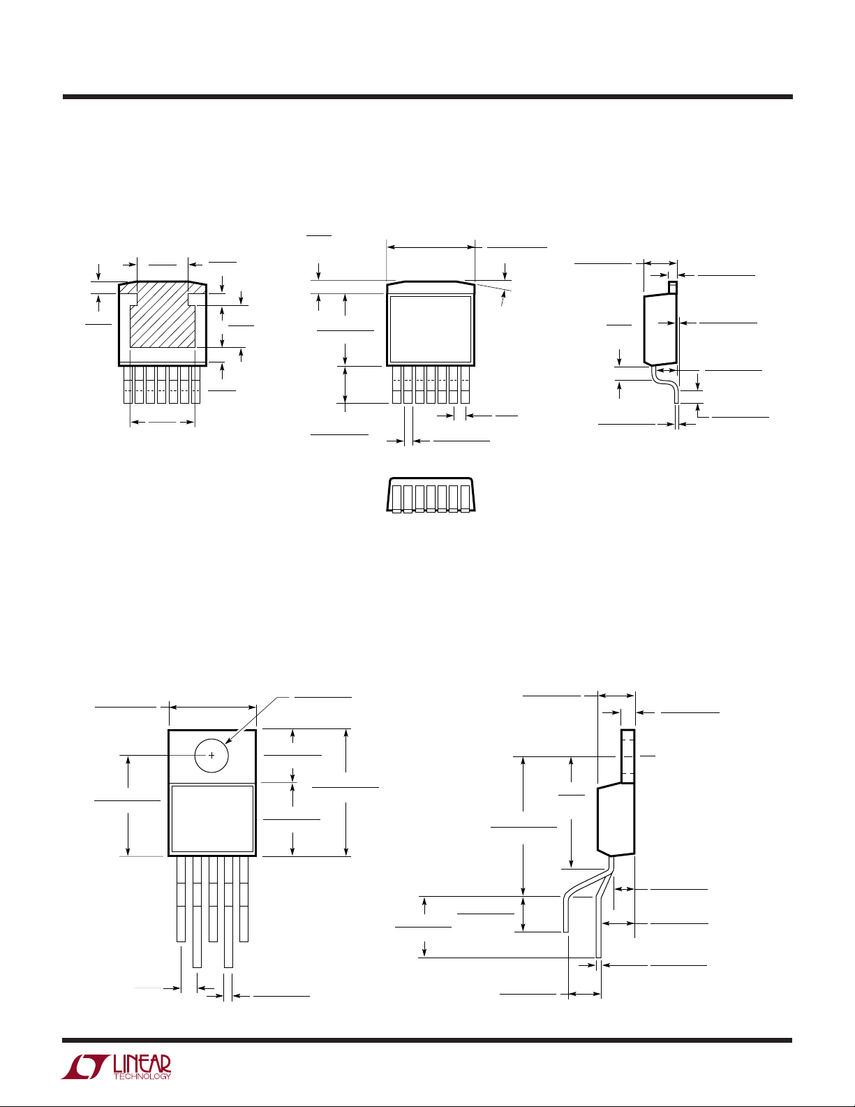
PACKAGE DESCRIPTIO
U
Dimensions in inches (millimeters) unless otherwise noted.
K Package
4-Lead TO-3 Metal Can
(LTC DWG # 05-08-1311)
0.320 – 0.350
(8.13 – 8.89)
0.420 – 0.480
(10.67 – 12.19)
0.760 – 0.775
(19.30 – 19.69)
0.038 – 0.043
(0.965 – 1.09)
1.177 – 1.197
(29.90 – 30.40)
72°
18°
0.470 TP
P.C.D.
0.060 – 0.135
(1.524 – 3.429)
0.655 – 0.675
(16.64 – 19.05)
0.151 – 0.161
(3.84 – 4.09)
DIA 2 PLC
0.167 – 0.177
(4.24 – 4.49)
R
0.490 – 0.510
(12.45 – 12.95)
R
K4(TO-3) 1098
0.256
(6.502)
0.060
(1.524)
0.300
(7.620)
BOTTOM VIEW OF DD PAK
HATCHED AREA IS SOLDER PLATED
COPPER HEAT SINK
14
0.060
(1.524)
0.075
(1.905)
0.183
(4.648)
Q Package
5-Lead Plastic DD Pak
(LTC DWG # 05-08-1461)
0.060
(1.524)
TYP
0.330 – 0.370
(8.382 – 9.398)
+0.012
0.143
–0.020
+0.305
3.632
()
–0.508
0.028 – 0.038
(0.711 – 0.965)
0.390 – 0.415
(9.906 – 10.541)
15
° TYP
0.067
(1.70)
BSC
0.165 – 0.180
(4.191 – 4.572)
0.059
(1.499)
TYP
0.013 – 0.023
(0.330 – 0.584)
0.045 – 0.055
(1.143 – 1.397)
+0.008
0.004
–0.004
+0.203
0.102
()
–0.102
0.095 – 0.115
(2.413 – 2.921)
± 0.012
0.050
(1.270 ± 0.305)
Q(DD5) 1098
PACKAGE DESCRIPTIO
LT1074/LT1076
U
Dimensions in inches (millimeters) unless otherwise noted.
R Package
7-Lead Plastic DD Pak
(LTC DWG # 05-08-1462)
0.256
(6.502)
0.060
(1.524)
0.300
(7.620)
BOTTOM VIEW OF DD PAK
HATCHED AREA IS SOLDER PLATED
COPPER HEAT SINK
(1.524)
(1.905)
0.060
0.075
0.183
(4.648)
0.060
(1.524)
TYP
0.330 – 0.370
(8.382 – 9.398)
+0.012
0.143
–0.020
+0.305
3.632
()
–0.508
0.026 – 0.036
(0.660 – 0.914)
0.390 – 0.415
(9.906 – 10.541)
15
° TYP
0.050
(1.27)
BSC
0.165 – 0.180
(4.191 – 4.572)
T Package
5-Lead Plastic TO-220 (Standard)
(LTC DWG # 05-08-1421)
0.059
(1.499)
TYP
0.013 – 0.023
(0.330 – 0.584)
0.045 – 0.055
(1.143 – 1.397)
+0.008
0.004
–0.004
+0.203
0.102
()
–0.102
0.095 – 0.115
(2.413 – 2.921)
± 0.012
0.050
(1.270 ± 0.305)
R (DD7) 1098
0.390 – 0.415
(9.906 – 10.541)
0.460 – 0.500
(11.684 – 12.700)
0.067
BSC
(1.70)
0.147 – 0.155
(3.734 – 3.937)
DIA
0.230 – 0.270
(5.842 – 6.858)
0.570 – 0.620
(14.478 – 15.748)
0.330 – 0.370
(8.382 – 9.398)
SEATING PLANE
0.152 – 0.202
0.260 – 0.320
(6.60 – 8.13)
0.028 – 0.038
(0.711 – 0.965)
Information furnished by Linear Technology Corporation is believed to be accurate and reliable.
However, no responsibility is assumed for its use. Linear Technology Corporation makes no representation that the interconnection of its circuits as described herein will not infringe on existing patent rights.
(3.861 – 5.131)
0.165 – 0.180
(4.191 – 4.572)
0.700 – 0.728
(17.78 – 18.491)
0.135 – 0.165
(3.429 – 4.191)
0.620
(15.75)
TYP
* MEASURED AT THE SEATING PLANE
0.045 – 0.055
(1.143 – 1.397)
0.095 – 0.115
(2.413 – 2.921)
0.155 – 0.195*
(3.937 – 4.953)
0.013 – 0.023
(0.330 – 0.584)
T5 (TO-220) 0399
15

LT1074/LT1076
TYPICAL APPLICATIO
U
Negative Boost Converter
200µF
V
–5V TO –15V
PACKAGE DESCRIPTIO
0.390 – 0.415
(9.906 – 10.541)
R1
12.7k
R2
2.21k
+
C1
100µF
1000
25V
D1*
+
5
µ
H
LT1074
GND
C3
+
15V
IN
MBR735
*
**
I
(MAX) = 1A TO 3A DEPENDING
OUT
ON INPUT VOLTAGE. SEE AN44
V
IN
V
FB
V
SW
V
C
C2
0.01µF
1nF
R3
750Ω
100pF
L1
25
µ
H
OPTIONAL OUTPUT FILTER
U
Dimensions in inches (millimeters) unless otherwise noted.
T7 Package
7-Lead Plastic TO-220 (Standard)
(LTC DWG # 05-08-1422)
0.147 – 0.155
(3.734 – 3.937)
DIA
0.165 – 0.180
(4.191 – 4.572)
µ
F
V
OUT
–15V**
LT1074 • TA04
0.045 – 0.055
(1.143 – 1.397)
0.230 – 0.270
(5.842 – 6.858)
0.460 – 0.500
(11.684 – 12.700)
0.050
BSC
(1.27)
0.330 – 0.370
(8.382 – 9.398)
0.026 – 0.036
(0.660 – 0.914)
0.570 – 0.620
(14.478 – 15.748)
0.260 – 0.320
(6.604 – 8.128)
SEATING PLANE
0.152 – 0.202
(3.860 – 5.130)
0.700 – 0.728
(17.780 – 18.491)
0.135 – 0.165
(3.429 – 4.191)
0.620
(15.75)
TYP
*MEASURED AT THE SEATING PLANE
0.095 – 0.115
(2.413 – 2.921)
0.155 – 0.195*
(3.937 – 4.953)
0.013 – 0.023
(0.330 – 0.584)
T7 (TO-220) 0399
RELATED PARTS
PART NUMBER DESCRIPTION COMMENTS
LT1375/LT1376 1.5A, 500kHz Step-Down Switching Regulators VIN Up to 25V, I
LT1374/LT1374HV 4.5A, 500kHz Step-Down Switching Regulators VIN Up to 25V (32V for HV), I
LT1370 6A, 500kHz High Efficiency Switching Regulator 6A/42V Internal Switch, 7-Lead DD/TO-220
LT1676 Wide Input Range, High Efficiency Step-Down Regulator VIN from 7.4V to 60V, I
LT1339 High Power Synchronous DC/DC Controller VIN Up to 60V, I
Up to 1.25A, SO-8
OUT
Up to 4.25A, SO-8/DD
OUT
Up to 0.5A, SO-8
OUT
Up to 50A, Current Mode
OUT
16
Linear Technology Corporation
1630 McCarthy Blvd., Milpitas, CA 95035-7417
(408) 432-1900 ● FAX: (408) 434-0507
●
www.linear-tech.com
1074fc LT/TP 0100 2K REV C • PRINTED IN USA
LINEAR TE CHNOLOGY CORPORATION 1994
 Loading...