

Page 1
DEMO MANUAL DC143
U
DESCRIPTIO
This demonstration circuit is a step-down (buck) regulator
using the LTC®1474/LTC1475. The exclusive use of surface
mount components and the LTC1474/LTC1475 in the tiny
MSOP package results in a highly efficient application in a
small board space. This demo board highlights the
capabilities of the LTC1474/LTC1475, which use a current
mode, constant off-time architecture to switch an internal
P-channel power MOSFET. This results in a power supply
that has low ripple and fast transient response. At low
output currents the LTC1474/LTC1475 automatically
switch to Burst ModeTM operation to maintain high operating
efficiencies and minimize supply current. At no load,only
DEMO MANUAL DC143
NO DESIGN SWITCHER
LTC1474/LTC1475
10µA I
, High Efficiency,
Q
Step-Down DC/DC
Converter
10µA (typical) is required to regulate the output. The parts
can be shut down to further reduce the supply current to
6µA (typical). In dropout, the internal P-channel MOSFET
is turned on continuously (100% duty cycle), providing
low dropout operation with V
battery detector allows the user to monitor the input
supply through an external resistive divider. This board is
intended for applications such as cellular phones, GSM
systems, 4mA to 20mA current-loop pirate supplies or any
portable battery-powered application. Gerber files for this
circuit board are available. Call the LTC factory.
, LTC and LT are registered trademarks of Linear Technology Corporation.
Burst Mode is a trademark of Linear Technology Corporation.
≅ VIN. An onboard low-
OUT
UW
WW
PERFORmANCE SU ARY
SYMBOL PARAMETER CONDITIONS BOARD SUFFIX VALUE
V
V
I
I
IN
OUT
OUT
Q
Input Voltage Range V
Output Voltage LTC1474/LTC1475 A, D 3.3V ± 0.10V
Maximum Output Current R
Typical Supply Current VIN = 10V, I
U
W
= 3.3V A, B, D, E 3.3V to 18V
OUT
= 5V C, F 5V to 18V
V
OUT
LTC1474-3.3/LTC1475-3.3 B, E 3.3V ± 0.10V
LTC1474-5/LTC1475-5 C, F 5V ± 0.15V
= 0Ω ALL 300mA
SENSE
= 0.25Ω ALL 150mA
R
SENSE
= 0 A, B, C 10µA
LOAD
V
IN
= 10V, I
= 0 D, E, F 15µA
LOAD
U
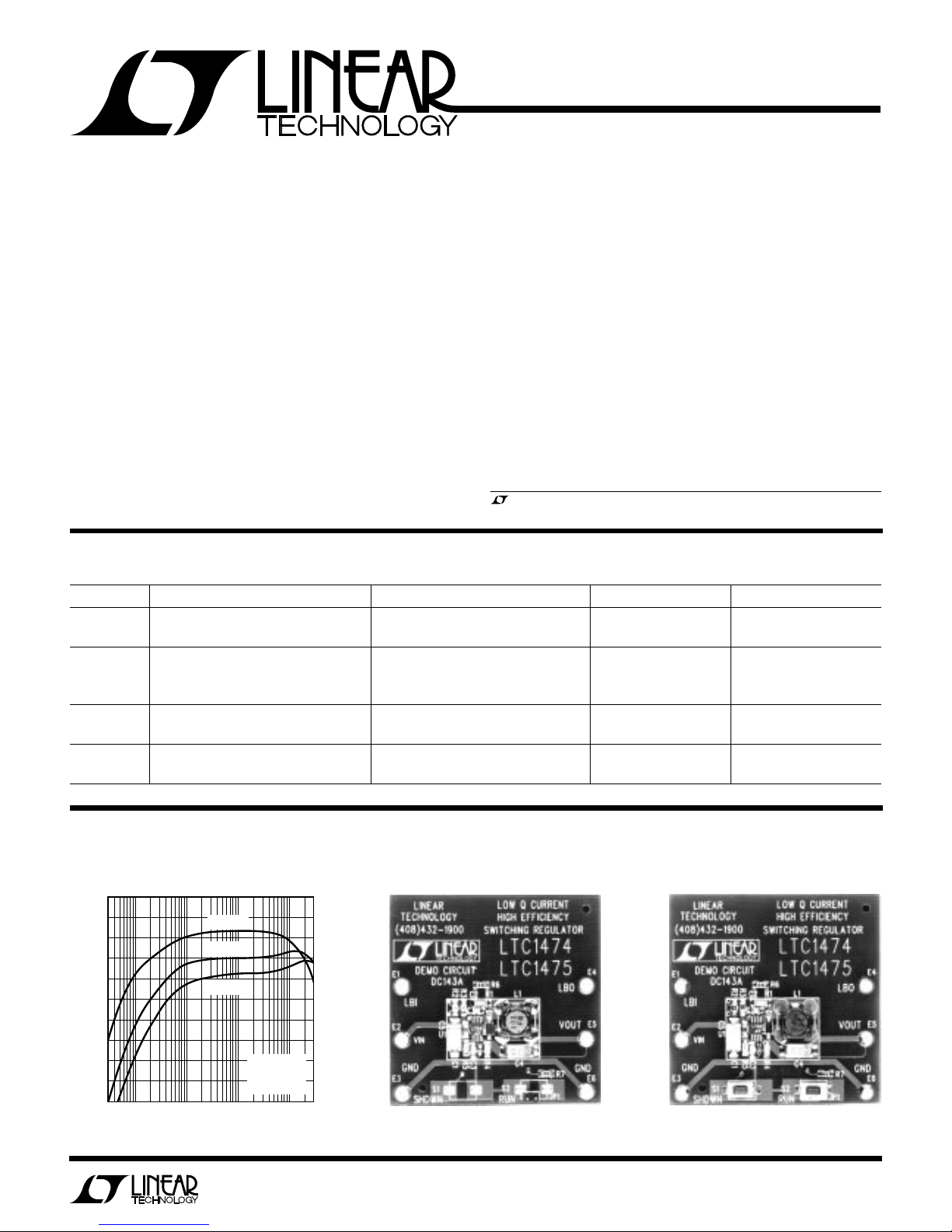
TYPICAL PERFOR A CE CHARACTERISTICS A D BOARD PHOTO
Board A, B, D, E Efficiency Demo Board A
100
VIN = 5V
90
80
VIN = 10V
VIN = 15V
Demo Board D
70
EFFICIENCY (%)
60
50
0.03 3 30 300
0.3
LOAD CURRENT (mA)
L = 100µH
= 3.3V
V
OUT
R
= 0Ω
SENSE
DM143 TPC
DM143 DB A
DM143 DB D
1
Page 2
DEMO MANUAL DC143
1
2
3
4
V
OUT
(VFB*)
LBO
LBI
GND
8
7
6
5
RUN
V
IN
SENSE
SW
TOP VIEW
MS8 PACKAGE
8-LEAD PLASTIC MSOP
*ADJUSTABLE OUTPUT VERSION
UW
WW
PERFORmANCE SU ARY
SYMBOL PARAMETER CONDITIONS BOARD SUFFIX VALUE
V
RIPPLE
∆V
V
LBI
OUT
Typical Output Ripple I
Typical Line Regulation 4V < VIN < 18V, R
Typical Load Regulation 0 < I
= 100mA All 50mV
OUT
< 18V, R
4V < V
IN
4V < VIN < 18V, R
4V < VIN < 18V, R
6V < VIN < 18V, R
< 18V, R
6V < V
IN
< 300mA, R
LOAD
0 < I
< 150mA, R
LOAD
SENSE
SENSE
SENSE
SENSE
SENSE
SENSE
= 0Ω, I
= 0.25Ω, I
= 0Ω, I
= 0.25Ω, I
= 0Ω, I
= 0.25Ω, I
SENSE
SENSE
= 100mA A, D 35mV
LOAD
= 100mA 25mV
LOAD
= 100mA B, E 20mV
LOAD
= 100mA 10mV
LOAD
= 100mA C, F 20mV
LOAD
= 100mA 10mV
LOAD
= 0Ω, VIN = 10V All 10mV
= 0.25Ω, VIN = 10V 10mV
Low-Battery Trip Threshold All 1.23V
W UW
PACKAGE A D SCHE ATIC DIAGRA SM
VIN
4V* TO 18V
LBI
*3.3V AT NO LOAD
4.7µF
35V
C3
+
C1
R6
0Ω
JP1
RUN
R1
0.25Ω
R7
100k
C2
1000pF
6
3
8
SENSE
LBI
RUN
7
V
IN
LTC1474
GND
4
V
LBO
SW
0.1µF
FB
C5
1
2
5
10pF
R5
R4
THIS NETWORK
IS PRESENT IN
BOARD A ONLY
+
L1
100µH
D1
MBR0530
C4
100µF
6.3V
V
OUT
3.3V
300mA
LBO
DM143 F01
LTC1474CMS8
LTC1474CMS8-3.3
LTC1474CMS8-5
Figure 1. LTC1474 Demo Board Schematic
VIN
4V* TO 18V
4.7µF
LBI
*3.3V AT NO LOAD
35V
+
C1
3.01M
1M
R3
R2
R6
0Ω
SHDN
R1
0.25Ω
R7
100kRUN
C2
1000pF
Figure 2. LTC1475 Demo Board Schematic
2
6
3
8
SENSE
LBI/OFF
ON
7
V
IN
LTC1475
GND
4
V
LBO
SW
0.1µF
FB
C3
C5
1
2
5
10pF
R5
R4
THIS NETWORK
IS PRESENT IN
BOARD D ONLY
+
L1
100µH
D1
MBR0530
C4
100µF
6.3V
V
OUT (VFB
LBO
LBI/OFF
GND
V
OUT
3.3V
300mA
*ADJUSTABLE OUTPUT VERSION
TOP VIEW
1
*)
2
3
4
MS8 PACKAGE
8-LEAD PLASTIC MSOP
LTC1475CMS8
LTC1475CMS8-3.3
8
7
6
5
ON
V
IN
SENSE
SW
LTC1475CMS8-5
LBO
DM143 F02
Page 3
DEMO MANUAL DC143
PARTS LIST
REFERENCE
DESIGNATOR QUANTITY PART NUMBER DESCRIPTION VENDOR TELEPHONE
C1 1 TPSC475M035 4.7µF 35V 20% Tantalum Capacitor AVX (207) 282-5111
C2 1 080553102KAT2A 1000pF 25V 10% X7R Capacitor AVX (803) 946-0362
C3 1 08055310KAT1A 10pF 25V 10% NPO Capacitor (Boards B, C, E, F Only) AVX (803) 946-0362
C4 1 TPSC107M006R0150 100µF 6.3V 20% Tantalum Capacitor (Boards A, B, D, E) AVX (207) 282-5111
TPSC336M010R0375 33µF 6.3V 20% Tantalum Capacitor (Boards C, F)
C5 1 08053E104ZAT1A 0.1µF 25V +80% to –20% Y5V Capacitor AVX (803) 946-0362
D1 1 MBR0530 0.5A 30V Schottky Diode Motorola (602) 244-3576
E1 to E6 6 2501-02 Terminal Turret Mill Max (516) 922-6000
JP1 1 2802S-02-G2 Connector Pin Header (Boards A, B, C) Comm Con (818) 301-4200
L1 1 CDRH73-101 100µH Inductor Sumida (847) 956-0666
R1 1 LR1206 01 R250 F0 0.25Ω 0.25W 1% Resistor IRC (512) 992-7900
R2 1 CR21-105J-T 1M 0.1W 5% Resistor (Boards D, E, F Only) AVX (803) 946-0524
R3 1 CR21-225J-T 2.2M 0.1W 5% Resistor (Boards D, E, F Only) AVX (803) 946-0524
R4 1 WCR0805-1474-F-P-LT 1.47M 0.1W 1% Resistor (Boards B, C, E, F Only) IRC (512) 992-7900
R5 1 CJ21-000J-T 0805 Shunt Resistor (Boards B, C, E, F) AVX (803) 946-0524
WCR0805-2494-F-P-LT 2.49M 0.1W 1% Resistor (Boards A, D) IRC (512) 992-7900
R6 1 CJ21-000J-T 0805 Shunt Resistor AVX (803) 946-0524
R7 1 CR21-104J-T 100k 0.1W 5% Resistor AVX (803) 946-0524
S1, S2 2 EVQ PJS05K Momentary Switch (Boards D, E, F) Panasonic (201) 392-4511
U1 1 LTC1474CMS8 8-Pin MSOP IC, LTC1474 (Board A) LTC (408) 432-1900
LTC1474CMS8-3.3 8-Pin MSOP IC, LTC1474-3.3 (Board B)
LTC1474CMS8-5 8-Pin MSOP IC, LTC1474-5 (Board C)
LTC1475CMS8 8-Pin MSOP IC, LTC1475 (Board D)
LTC1475CMS8-3.3 8-Pin MSOP IC, LTC1475-3.3 (Board E)
LTC1475CMS8-5 8-Pin MSOP IC, LTC1475-5 (Board F)
Table 1. Demo Board Version Cross Reference
BOARD SUFFIX PART NUMBER OUTPUT VOLTAGE ON/OFF CONTROL
A LTC1474 3.3V (Adjustable) Jumper
B LTC1474-3.3 3.3V Jumper
C LTC1474-5 5V Jumper
D LTC1475 3.3V (Adjustable) Pushbutton
E LTC1475-3.3 3.3V Pushbutton
F LTC1475-5 5V Pushbutton
3
Page 4

DEMO MANUAL DC143
QUICK START GUIDE
Demonstration Board DC143 is easy to set up for
evaluation of the LTC1474/LTC1475. Please follow the
procedure below for proper operation:
●
Connect the input power supply to the VIN and GND
terminals.
●
The LBO pin is a current sinking pin. When the LBI pin
goes below 1.23V, the LBO pin will sink 0.7mA of
current.
●
The LBI pin is the low-battery detector input pin.
Normally, its input comes from the input voltage
U
OPERATIO
The circuits shown in Figures 1 and 2 operate from input
voltages of 3.3V to 18V. The six different versions of the
demo board provide 3.3V or 5V, as specified in Table 1. For
output voltages other than 3.3V or 5V, use Board A or D
and change the resistive divider R4/R5 to the appropriate
ratio. For output voltages lower than 3V, input voltages as
low as 3V can be used. The demo boards provide two
on/off options— by opening or shorting jumper JP1
(Boards A, B and C) or push-button (Boards D, E and F).
Operation
The LTC1474/LTC1475 use a current mode, constant offtime architecture shown in Figure 3. Current mode operation provides the well known advantages of clean start-up
and excellent line and load regulation. Constant off-time
adds to this list simplicity (neither an oscillator nor ramp
compensation is required) and inherent 100% duty cycle
in dropout.
The LTC1474/LTC1475 use Burst Mode operation to keep
the output capacitor charged to the proper output voltage
while minimizing quiescent current. Burst Mode operation
works by using short burst cycles to keep the output
capacitor charged, followed by a “sleep” mode where the
load current is supplied by the output capacitor and the
LTC1474/LTC1475 draw only 9µA of supply current.
Because of Burst Mode operation and the constant
off-time, the frequency changes with input voltage and
through a resistor network (the resistor divider is
present only on boards D, E and F).
●
Connect the load between the V
Refer to Figure 6 for proper measurement equipment
setup.
●
For board A, B or C, open jumper JP1 to turn on or short
the jumper to shut down. For Board C, D or E,
momentarily depress the RUN push-button to turn on
or momentarily depress the SHDN push-button to shut
down.
load. During sleep mode, the low quiescent current is
achieved by turning on only the voltage comparator and
voltage reference, which are needed to monitor the output
voltage, and the low-battery comparator. The low quiescent current and variable frequency minimize losses that
would normally dominate at light loads (DC supply current
losses and switching losses due to the MOSFET switch
gate charge). This results in the high efficiencies down to
extremely light loads and the ultralow supply current
required to maintain the output voltage at no load.
The LTC1474/LTC1475 also provide user-programmable
peak inductor current: the user can set the peak current to
any value between 10mA and 400mA with the appropriate
sense resistor. At the beginning of the burst cycle, the
internal P-channel MOSFET switch is turned on, causing
the inductor current to begin to increase. This current
flows through both an internal and an optional external
sense resistor. The internal current comparator monitors
the voltage drop across the sense resistors and, when the
voltage reaches 100mV, the current comparator trips and
turns the switch off, causing the inductor current to
decrease. At the end of the 4.75µs off-time, the switch
either turns back on or stays off (sleep mode), depending
on the status of the voltage comparator. Without an
external sense resistor (Pins 6 and 7 shorted), the peak
current defaults to the 400mA max due to the internal
sense resistor.
and GND terminals.
OUT
4
Page 5

OPERATIO
1µA
LTC1474: RUN
LTC1475: ON
8
2
LBO
CONNECTION NOT PRESENT IN LTC1474 SERIES
×
CONNECTION PRESENT IN LTC1474 SERIES ONLY
U
LBI/OFF
1-SHOT
TRIGGER OUT
V
ON
FB
LB
×
4.75µs
+
–
3
READY
LTC1474: LBI
LTC1475: LBI/OFF
ON
ON
C
–
+
–
V
+
1.23V
REFERENCE
100mV
1.23V
DEMO MANUAL DC143
V
IN
7
R
SENSE
(OPTIONAL)
V
CC
5Ω
1×
GND
4
25×
SENSE
6
SW
5
V
FB
1
V
IN
+
V
OUT
+
DM143 F03
Figure 3. LTC1474/LTC1475 Block Diagram
The demo board includes two sense resistors; 0.25Ω R1
is shorted out with a 0Ω resistor (R6) to easily demonstrate
peak current programming. With the short in place (R
SENSE
= 0Ω), the peak current is the maximum 400mA providing
a maximum load of 300mA. With the short removed
(R
= 0.25Ω), the peak current is reduced to 200mA
SENSE
and the maximum load is 150mA.
Low-Battery Detector
The low-battery indicator senses the input voltage through
an external resistive divider. This divided voltage connects
to the (–) input of a voltage comparator (Pin 3), which is
compared with a 1.23V reference voltage. Because the
current going into Pin 3 is negligible, the following
expression is used for setting the trip point:
V
= 1.23(1 + R3/R2)
LBTRIP
(Ω)
SENSE
R
5
4
3
2
1
0
0
100 150 200
50
MAXIMUM OUTPUT CURRENT (mA)
Figure 4. R
SENSE
250 300
DM143 F04
Selection
5
Page 6

DEMO MANUAL DC143
U
OPERATIO
V
IN
R3
LBI
R2
Figure 5. Low-Battery Comparator
LTC1474/LTC1475
–
+
1.23V
REFERENCE
DM143 F05
LBO
LBI
A
+
Figure 6. Correct Measurement Setup
V
IN
V
GND
LBO
V
OUT
GND
A
V
LOAD
DM143 F06
HOW TO MEASURE VOLTAGE REGULATION
When trying to measure voltage regulation, remember
that all measurements must be taken at the point of
regulation. This point is where the LTC1474/LTC1475’s
control loop looks for the information to keep the output
voltage constant. This information occurs between Pins 1
and 4 of the LTC1474/LTC1475. These points correspond
to the output terminals of the demonstration board. Test
leads should be attached to these terminals. Measurements should not be taken at the end of test leads at the
load. Refer to Figure 6 for proper monitoring equipment
configuration. This applies to line regulation (input-tooutput voltage regulation) as well as load regulation tests.
In doing line regulation tests, always look at the input
voltage across the input terminals.
For the purposes of these tests, the demonstration circuit
should be fed from a regulated DC bench supply so
additional variation on the DC input does not add an error
to the regulation measurements.
For measurement of no-load supply current and measurement of efficiency at loads below 1mA,
the input impedance of the voltmeters may have a significant effect on
measurements
. For example, in the case of voltmeters
with 10MΩ impedance, the no-load supply current at
VIN = 15V will increase from 10.5µA with no meters
connected to 12µA with meters connected to both the
input and output. Likewise, with VIN = 15V and I
LOAD
=
100µA, the efficiency decreases from 59% to 56.8% when
the voltmeters are connected. Therefore, for the most
accurate measurements at light loads, first record the
voltmeter readings, then disconnect the voltmeters before
making the input supply current measurement.
COMPONENTS
Component selection can be very critical in switching
power supply applications. This section discusses some
of the guidlines for selecting the different components.
The LTC1474/LTC1475 data sheet details more specific
selection criteria for most of the external components
surrounding the IC. Be sure to refer to the data sheet if
changes to this demo circuit are anticipated.
Capacitors
The most common component uncertainty with switching
power supplies involves capacitors. In this circuit (refer to
Figure 1) C1 and C4 are low ESR, high ripple current
tantalum capacitors specifically designed and developed
for use in switching power supplies. ESR (equivalent
series resistance) is the parasitic series resistance in the
capacitor. Often, this resistance is the limiting element in
reducing ripple at the output or input of the supply.
Other choices are organic semiconductor type capacitors
(OS-CON) that are specifically made for power supply
applications. For lower current applications (<50mA)
ceramic capacitors, available as large as 10µ F, provide the
smallest size and lowest ESR.
Normal tantalums are not recommended for use in these
applications (especially the low cost ones), as they do not
have the ability to take the large peak currents that are
required for the application. Standard wet electrolytics
also may not meet requirements, due to their high ESR,
limited operating life and larger size.
6
Page 7

OPERATIO
DEMO MANUAL DC143
U
Inductor
Many off-the-shelf surface mount inductors are available
that work well in LTC1474/LTC1475 applications. The
inductor used in this demo board is from Sumida, but
there is a wide variety of inductors available from other
manufacturers, such as the Dale LPT4545 series, Coilcraft
DO1608 and DO3316 series and Coiltronics CTX series.
The inductors vary in size, shape, cost, current rating and
loss characteristics. The only fixed requirement of the
inductor is that it must be able to support the output DC
current and still maintain its inductance value. The other
variables need to be traded off against the requirements
for area, efficiency and cost in choosing the optimal
inductor.
Sense Resistor
The demo board is provided with a 0.25Ω current sense
resistor—a special, low valued, current shunt resistor
made by IRC. However, in most cases the least expensive
solution is obtained by paralleling standard resistors (available in values ≥ 1Ω) instead of using this special low
valued resistor. Although a single resistor could be used
with the desired value, these low valued resistor types are
much more expensive and are currently not available in
case sizes smaller than 1206. Three or four 0603 size
standard resistors require about the same area as one
1206 size low valued resistor and are available at a fraction
of the cost.
Schottky Diode
The catch diode carries load current during the off-time.
The average diode current is therefore dependent on the
P-channel switch duty cycle. At high input voltages the
diode conducts most of the time. As VIN approaches V
OUT
the diode conducts only a small fraction of the time. The
most stressful condition for the diode is when the output
is short-circuited. Under this condition, the diode must
safely handle I
at close to 100% duty cycle.
PEAK
To maximize both low and high current efficiency, a fast
switching diode with low forward drop and low reverse
leakage should be used.
Low reverse leakage current is
critical to maximize low current efficiency, since the leakage can potentially approach the magnitude of the LTC1474/
LTC1475 supply current.
Low forward drop is critical for
high current efficiency, since loss is proportional to forward drop. These are conflicting parameters, but a good
compromise is the MBR0530 0.5A Schottky diode specified in the schematic. Using a diode with slightly lower
forward drop, for example the MBRS130, increases the
efficiency by 1.3%, but also increases the no-load suppy
current from 10µA to 16µA.
Component Manufacturers
Beside the components that are used on the demonstration board, other components may also be used. Below is
a partial list of the manufacturers whose components you
can use for the switching regulator. Using components
other than the ones on the demonstration board requires
recharacterizing the circuit for efficiency.
MANUFACTURER COMPONENT PART NUMBERS TELEPHONE FAX
Coilcraft Inductors DO1608, DO3316 Series (847) 639-6400 (847) 639-1469
Coiltronics International Inductors Econo-Pac, Octa-Pac (561) 241-7876 (561) 241-9339
Dale Electronics Inductors LPT4545 (605) 665-9301 (605) 665-1627
Sumida Electric Co. Ltd Inductors CD54, CDRH74B Series (847) 956-0666 (847) 956-0702
AVX Corporation Capacitors TPS/TAJ Series, AA Series (803) 448-9411 (803) 448-1943
Sanyo Video Components Capacitors OS-CON Series (619) 661-6835 (619) 661-1055
Sprague Capacitors 593D Series (207) 324-4140 (207) 324-7223
Marcon Capacitors THC Series (847) 696-2000 (847) 518-9985
Information furnished by Linear Technology Corporation is believed to be accurate and reliable.
However, no responsibility is assumed for its use. Linear Technology Corporation makes no representation that the interconnection of its circuits as described herein will not infringe on existing patent rights.
7
Page 8

DEMO MANUAL DC143
UW
PCB LAYOUT A D FIL
Component Side Silkscreen Component Side
Solder Side
U
PC FAB DRAWI G
2.000
B
C
C
C
B
AA
C
2.000
C
C
Component Side Solder Mask
Solder Side Solder Mask
DIAMETER NUMBER OF
SYMBOL (INCH) HOLES PLATED
UNMARKED 0.015 11 YES
A 0.030 2 YES
B 0.070 2 NO
C 0.094 6 YES
TOTAL HOLES 21
NOTES:
1. MATERIAL IS FR4, 0.062” THICK WITH 2 OZ COPPER
2. PCB WILL BE DOUBLE-SIDED WITH PLATED THROUGH HOLES
3. PLATED THROUGH HOLE — WALL THICKNESS MIN 0.0014” (1 oz)
4. SOLDER MASK BOTH SIDES
5. SILKSCREEEN COMPONENT SIDE
6. ALL HOLE SIZES AFTER PLATING +0.003/–0
Linear Technology Corporation
8
1630 McCarthy Blvd., Milpitas, CA 95035-7417 ● (408) 432-1900
FAX: (408) 434-0507
●
TELEX: 499-3977 ● www.linear-tech.com
dc143 LT/TP 0697 500 • PRINTED IN USA
LINEAR TECHNOLOGY CORPORATION 1997
 Loading...