

Page 1
DEMO MANUAL DC1832A
LT3995
60V, 3A, 2MHz Step-Down
Switching Regulator with
Description
Demonstration circuit 1832A is a monolithic step-down
DC/DC switching regulator featuring the LT3995. The
LT3995 is a compact, high efficiency monolithic step-down
switching regulator that consumes only 2.7μA of quiescent
current. The demo circuit is designed for 3.3V, 3A output
from a 4.3V to 60V input. The switching frequency can be
programmed either via oscillator resistor or external clock
up to 2MHz. To synchronize to an external clock, move
JP2 to SYNC and apply the external clock to the SYNC
turret. The RT resistor (R5) should be chosen to set the
LT3995 internal switching frequency at least 20% below
the lowest synchronization input frequency.
®
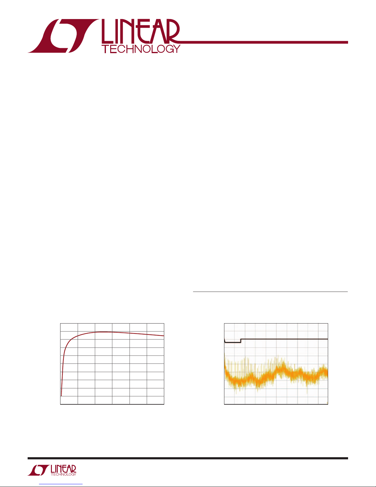
Low ripple Burst Mode
ciency at the light load while keeping the output ripple
below 15mV. The SYNC pin on the demo board is grounded
by default by setting JP2 at RT FREQ for low ripple
Burst Mode operation. Figure1 shows the demo board
efficiency at 12V input voltage.
The LT3995 is in shutdown when the EN pin is low and
active when the pin is high. The threshold of the EN pin
is accurate at 1.02V with 60mV of hysteresis. Users can
populate R7 and R8 to provide a programmable under
operation increases the effi-
2.7µA Quiescent Current
voltage lockout. A low dropout voltage of 500mV is maintained when the input voltage drops below the programmed
output voltage. During a short-circuit fault, the LT3995
has current limit foldback to limit the power dissipation.
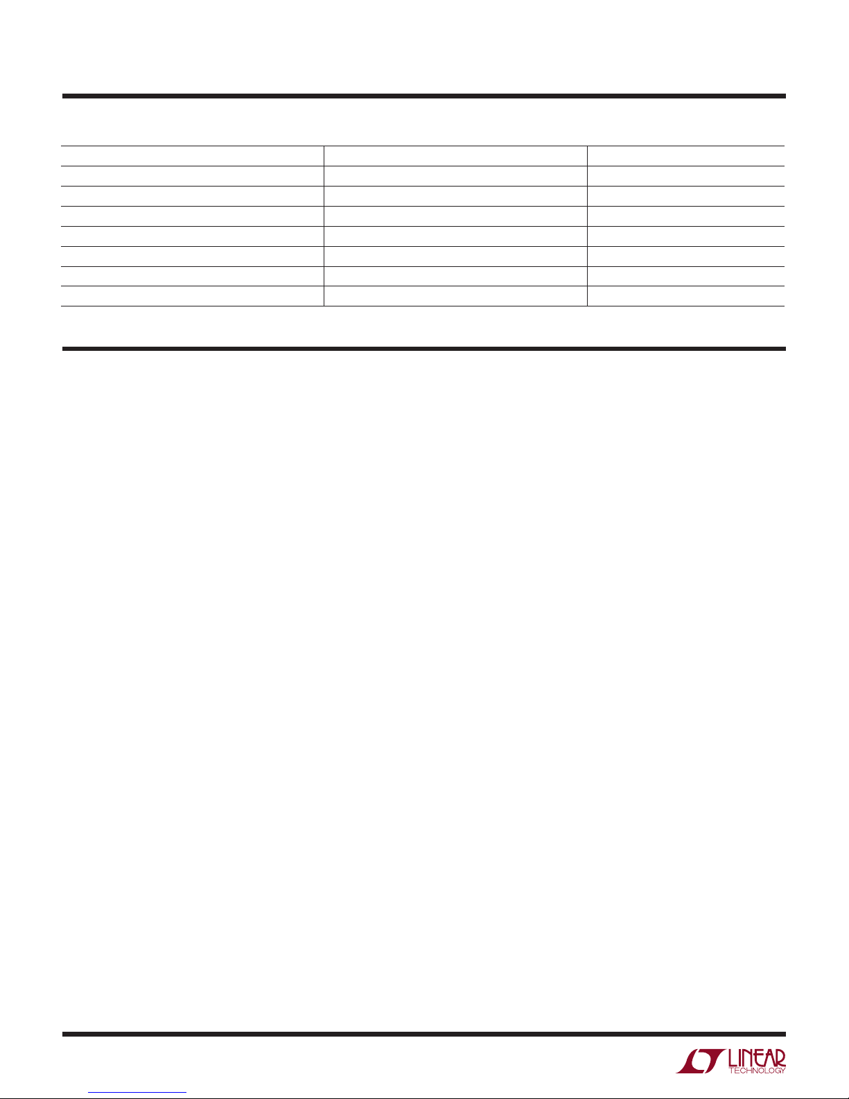
The demo board has an EMI filter installed. The EMI
performance of the demo board at 12V input voltage is
shown on Figure 2. The limit in Figure 2 is EN55022 Class
B. The figure shows the circuit passes the test with a wide
margin. To use the EMI filter, the input should be tied to
VEMI not V
The LT3995 data sheet gives a complete description of
the part, operation and application information. The data
sheet must be read in conjunction with this demo manual
for demo circuit 1832A. The LT3995 is assembled in a 16lead plastic MSOP package with an exposed pad for low
thermal resistance. Proper board layout is essential for
both proper operation and maximum thermal performance.
See the data sheet sections for details.
Design files for this circuit board are available at
http://www.linear.com/demo
L, LT, LTC, LTM, Linear Technology, the Linear logo and Burst Mode are registered
trademarks of Linear Technology Corporation. All other trademarks are the property of their
respective owners.
IN
.
90
85
80
75
70
65
60
EFFICIENCY (%)
55
50
45
40
0
0.5
Figure 1. LT3995 Efficiency vs Load Current,
12VIN to 3.3V
OUT
1.5 2 2.5
1
LOAD CURRENT (A)
Efficiency
dc1832a F01
70
TRACE 1 PASS
60
50
40
30
20
10
0
–10
10dB/DIV LOG, REF 70.00dBµV
–20
3
–30
START 150kHz
RES BW (CISPR) 9kHz
Figure 2. LT3995 Demo Board EMI Performance
(Switching Frequency = 300kHz, VIN = 12V)
VBW 62kHz
STOP 30.00 MHz
SWEEP 717ms (6637pts)
dc1832a F02
dc1832af
1
Page 2
DEMO MANUAL DC1832A
performance summary
PARAMETER CONDITIONS VALUE
Guaranteed Minimum Input Voltage 4.3V
Maximum Input Voltage 60V
Output Voltage V
Switching Frequency R
Guaranteed Maximum Output Current I
Typical Efficiency V
Typical Output Voltage Ripple V
OUT
OUT
Specifications are at TA = 25°C
VIN = 4.3V ~ 60V 3.275V ± 3%
= 182k 300kHz ± 20%
T
VIN = 4.3V ~ 60V 3A
= 12V, I
IN
= 12V, I
IN
= 3A 82.2%
OUT
= 3A 11mV
OUT
Quick start proceDure
Demonstration circuit 1832A is easy to set up to evaluate the performance of the LT3995. Refer to Figure 3
for proper measurement equipment setup and use the
following procedure.
NOTE. When measuring the input or output voltage ripple,
care must be taken to avoid a long ground lead on the
oscilloscope probe. Measure the input or output voltage
ripple by touching the probe tip directly across the V
or V
and GND terminals. See Figure 4 for the proper
OUT
scope technique.
1. Place JP1 on the ON position.
4. With power off, connect load from V
5. Turn on the power at the input.
6. Check for the proper output voltage (3.3V).
NOTE. If there is no output, temporarily disconnect the
load to make sure that the load is not set too high or
is shorted.
IN
7. Once the proper output voltage is established, adjust
the load within the operating ranges and observe the
output voltage regulation, ripple voltage, efficiency and
other parameters.
OUT
to GND.
2. Place JP2 on the RT FREQ position.
3. With power off, connect the input power supply to V
and GND. Make sure that the input voltage does not
exceed 60V.
8. An external clock
when SYNC function is used (JP2 on the SYNC position). Please make sure that the SYNC frequency is at
IN
least 20% higher than the set switching frequency.
See the data sheet Synchronization section.
can be added to the SYNC terminal
dc1832af
2
Page 3

Quick start proceDure
DEMO MANUAL DC1832A
Figure 3. Proper Measurement Equipment Setup
Figure 4. Measuring Input or Output Ripple
dc1832af
3
Page 4

DEMO MANUAL DC1832A
parts List
ITEM QTY REFERENCE PART DESCRIPTION MANUFACTURER/PART NUMBER
Required Circuit Components
1 2 C1, C8 CAP., X5R, 47µF, 10V, 20%, 1210 TDK, C3225X5R1A476M
2 1 C2 CAP., X5R, 0.47µF, 25V, 10%, 0603 TDK, C1608X5R1E474M
3 2 C3, C7 CAP., X7R, 2.2µF, 100V, 10%,1210 TDK, C3225X7R2A225M
4 1 C5 CAP., C0G, 10pF, 50V, 10%, 0402 TDK, C1005C0G1H100D
5 1 C6 CAP., X7R, 10nF, 25V, 10%, 0402 TDK, C1005X7R1E103K
6 1 C11 CAP., X5R, 1µF, 10V, 10%, 0603 TDK, C1608X5R1A105K
7 1 C12 CAP., X7R, 0.1µF, 100V, 10%, 0603 MURATA, GRM188R72A104KA35D
8 1 D1 DIODE, PDS360 PowerDi5 DIODE INC., PDS360
9 1 L1 IND, 8.2µH COILCRAFT, XAL6060-822ME
10 1 R1 RES., CHIP, 1.00M, 1/16W, 1%, 0402 NIC, NRC04F1004TRF
11 1 R2 RES., CHIP, 576k, 1/16W, 1%, 0402 NIC, NRC04F5763TRF
12 1 R5 RES., CHIP, 182k, 1/16W, 1%, 0402 NIC, NRC04F1823TRF
13 1 R6 RES., CHIP, 200k, 1/16W, 1%, 0402 NIC, NRC04F2003TRF
14 1 U1 I.C., LT3995EMSE, MSE16 LINEAR TECHNOLOGY, LT3995EMSE
Additional Demo Board Circuit Components
1 1 C4 CAP., ALUM., 100µF, 100V, 10% SUN ELECT, 100CE100KXT
2 2 C9, C10 CAP., X7R, 2.2µF, 100V, 10%, 1210 TDK, C3225X7R2A225M
3 1 C13 CAP., HVP SERIES, 33µF, 63V, 20% SUNCON, 63HVP33M
4 1 L2 IND
5 1 L3 IND, 3.3µH VISHAY, IHLP-2020BZER3R3M01
6 0 R7,R8 RES., 0603 OPT
Hardware: For Demo Board Only
1 7 E1, E2, E3, E4, E5, E6, E7 TURRET, 0.094" MILL-MAX, 2501-2-00-80-00-00-07-0
2 2 E8, E9 TESTPOINT, TURRET, 0.061" PBF MILL-MAX, 2308-2-00-80-00-00-07-0
3 2 JP1, JP2 JMP, 1X3-079 SAMTEC, TMM-103-02-L-S
4 2 XJP1, XJP2 SHUNT, 2mm CTRS. SAMTEC, 2SN-BK-G
, 1.0µH VISHAY, IHLP-1616BZER1R0M01
4
dc1832af
Page 5

schematic Diagram
VOUT
VOUT
3.3V / 3A
3.3V / 3A
E1
E1
C11
1uF
10V
C11
1uF
10V
C8
47uF
10V
C8
47uF
10V
C1
47uF
10V
C1
47uF
10V
VOUT
0603
0603
1210
1210
1210
1210
GNDE2GND
DEMO MANUAL DC1832A
SYNCE7SYNC
E2
E7
SYNC
RT FREQ
SYNC
RT FREQ
JP2
JP2
132
VIN
L1
8.2uHL18.2uH
5
SW
U1
U1
LT3995EMSE
LT3995EMSE
10
C5
R1
D1
D1
C2
SW6SW
VIN11VIN
C12
C12
7
12
10pFC510pF
1.00M
1%R11.00M
1%
PDS360
PDS360
3
2 1
0.47uF
0603C20.47uF
0603
4
VIN
100V
100V
0.1uF
0.1uF
3
OUT
BOOST
PG
15
0603
0603
ALL CAPACITORS ARE IN MICROFARADS, 0402.
1. ALL RESISTORS ARE IN OHMS, 0402.
NOTE: UNLESS OTHERWISE SPECIFIED
R2
576k1%R2
576k
1%
R5
182k1%(300kHz)
R5
182k1%(300kHz)
1
14
16
FB
RT
SYNC
NC
9
GND
17
NC
8
SS2EN
13
C6
10nFC610nF
R6
200KR6200K
L3
L3
3.3uH
3.3uH
IND-IHLP2020BZ-01
IND-IHLP2020BZ-01
L2
L2
1.0uH
1.0uH
IND-IHLP1616BZ-01
IND-IHLP1616BZ-01
VEMIE8VEMI
R7
OPT
0603R7OPT
0603
63V
63V
C13
C13
33uF
33uF
63HVP33
63HVP33
+
+
C10
C10
2.2uF
1210
2.2uF
1210
100V
100V
C9
C9
2.2uF
1210
2.2uF
1210
100V
100V
E8
R8
OPT
0603R8OPT
0603
E9
GNDE9GND
C7
2.2uF
C7
2.2uF
C3
2.2uF
C3
2.2uF
C4
100uF
C4
100uF
+
+
VIN
E3
E3
VIN
VIN
4.3V - 60V
4.3V - 60V
Information furnished by Linear Technology Corporation is believed to be accurate and reliable.
However, no responsibility is assumed for its use. Linear Technology Corporation makes no representation that the interconnection of its circuits as described herein will not infringe on existing patent rights.
100V
100V
100V
100V
100V
100V
1210
1210
1210
1210
E4
GNDE4GND
SUNCON
100CE100KXT
E6PGE6PGE5
EN/UVLO
EN/UVLO
132
JP1
JP1
ON
ON
OFF
OFF
E5
dc1832af
5
Page 6

DEMO MANUAL DC1832A
DEMONSTRATION BOARD IMPORTANT NOTICE
Linear Technology Corporation (LT C) provides the enclosed product(s) under the following AS IS conditions:
This demonstration board (DEMO BOARD) kit being sold or provided by Linear Technology is intended for use for ENGINEERING DEVELOPMENT
OR EVALUATION PURPOSES ONLY and is not provided by LT C for commercial use. As such, the DEMO BOARD herein may not be complete
in terms of required design-, marketing-, and/or manufacturing-related protective considerations, including but not limited to product safety
measures typically found in finished commercial goods. As a prototype, this product does not fall within the scope of the European Union
directive on electromagnetic compatibility and therefore may or may not meet the technical requirements of the directive, or other regulations.
If this evaluation kit does not meet the specifications recited in the DEMO BOARD manual the kit may be returned within 30 days from the date
of delivery for a full refund. THE FOREGOING WARRANTY IS THE EXCLUSIVE WARRANTY MADE BY THE SELLER TO BUYER AND IS IN LIEU
OF ALL OTHER WARRANTIES, EXPRESSED, IMPLIED, OR STATUTORY, INCLUDING ANY WARRANTY OF MERCHANTABILITY OR FITNESS
FOR ANY PARTICULAR PURPOSE. EXCEPT TO THE EXTENT OF THIS INDEMNITY, NEITHER PARTY SHALL BE LIABLE TO THE OTHER FOR
ANY INDIRECT, SPECIAL, INCIDENTAL, OR CONSEQUENTIAL DAMAGES.
The user assumes all responsibility and liability for proper and safe handling of the goods. Further, the user releases LT C from all claims
arising from the handling or use of the goods. Due to the open construction of the product, it is the user’s responsibility to take any and all
appropriate precautions with regard to electrostatic discharge. Also be aware that the products herein may not be regulatory compliant or
agency certified (FCC, UL, CE, etc.).
No License is granted under any patent right or other intellectual property whatsoever. LT C assumes no liability for applications assistance,
customer product design, software performance, or infringement of patents or any other intellectual property rights of any kind.
LT C currently services a variety of customers for products around the world, and therefore this transaction is not exclusive.
Please read the DEMO BOARD manual prior to handling the product. Persons handling this product must have electronics training and
observe good laboratory practice standards. Common sense is encouraged.
This notice contains important safety information about temperatures and voltages. For further safety concerns, please contact a LTC application engineer.
Mailing Address:
Linear Technology
1630 McCarthy Blvd.
Milpitas, CA 95035
Copyright © 2004, Linear Technology Corporation
Linear Technology Corporation
6
1630 McCarthy Blvd., Milpitas, CA 95035-7417
(408) 432-1900 ● FAX: (408) 434-0507 ● www.linear.com
dc1832af
LT 0513 • PRINTED IN USA
LINEAR TECHNOLOGY CORPORATION 2013
 Loading...