

Page 1

QUICK START GUIDE FOR DEMONSTRATION CIRCUIT 620
HIGH CURRENT QUAD OUTPUT SWITCHING REGULATORS FOR TFT-LCD PANELS
LT1943
DESCRIPTION
Demonstration circuit 620 is a quad output power
supply intended for use in large TFT-LCD panels. The
circuit features the LT®1943 high current quad-output
switching regulator and generates a 3.3V logic supply
along with the triple output supply required for the
TFT-LCD panels. With an input voltage range of 8V to
20V, a step down regulator provides 3.3V VLOGIC with
up to 2A current; a high power SEPIC converter, a
lower power boost converter and an inverting
converter provide three independent output voltages
AVDD, VON and VOFF required by the LCD panels. A high
All four switchers are synchronized to the internal
1.2MHz clock, allowing the use of low profile
inductors and ceramic capacitors. They all have softstart to limit start-up inrush current.
Long wires run from input sources (such as wall
adaptors) can cause large voltage spikes during initial
plug-in. C17 is installed on DC620 to damp the
possible voltage spikes. C17 is not required for
applications when input source is close to the
regulator. Please refer to Application Note 88 for
details.
side PNP provides delayed turn on of the VON signal
and can source up to 30mA at 30V.
Design files for this circuit board are available.
Call the LTC factory.
LT is a registered trademark of Linear Technology Corporation
Table 1. Performance Summary (T
PARAMETER CONDITION VALUE
Minimum Input Voltage -40°C to 85°C 8V
Maximum Input Voltage -40°C to 85°C 20V
= 25°C unless otherwise noted)
A
Output Voltage V
Maximum Output Current at V
Typical Output Ripple V
Typical Output Ripple AVDD V
Typical Switching Frequency 1.2MHz
On/Off Control
Note 1: 2A maximum output current is guaranteed when V
rent at V
curve.
. More output current is available at higher input voltage. Please refer to the LT1943 data sheet for output current vs. input voltage
LOGIC
V
LOGIC
V
LOGIC
V
LOGIC
= 8V to 20V, I
IN
= 8V to 20V (Note 1) 2A
IN
= 12V, load at V
IN
= 12V, load at AVDD = 500mA (20MHz BW) 64mV
IN
Logic Low Voltage-Off, -40°C to 85°C 0.4V MAX
Logic High Voltage-On 2.4V MIN
is unloaded. Since V
OFF
= 0A to 2A 3.3V ±3%
OUT
= 2A (20MHz BW) 23mV
LOGIC
is supplied from V
OFF
, the load at V
LOGIC
QUICK START PROCEDURE
Demonstration circuit 620 is easy to set up to
evaluate the performance of the LT1943. Refer to
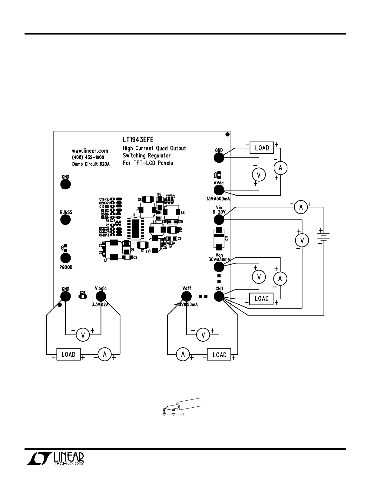
Figure 1 for proper measurement equipment setup
and follow the procedure below:
NOTE: When measuring the input or output
voltage ripple, care must be taken to avoid a long
ground lead on the oscilloscope probe. Measure
the input or output voltage ripple by touching the
P–P
P–P
reduces the available cur-
OFF
1
Page 2
QUICK START GUIDE FOR DEMONSTRATION CIRCUIT 620
HIGH CURRENT QUAD OUTPUT SWITCHING REGULATORS FOR TFT-LCD PANELS
probe tip directly across the VIN or V
OUT
GND terminals. See Figure 2 for proper scope
probe technique.
1.
Make sure the input voltage does not exceed 20V.
With power off, connect the input power supply to
VIN and GND.
2.
Turn on the power at the input.
and
3.
Check for the proper output voltages. If there is no
output, temporarily disconnect the load to make
sure that the load is not set too high.
4.
Once the proper output voltages are established,
adjust the loads within the operating range and observe the output voltage regulation, ripple voltage,
efficiency and other parameters.
Figure 1. Proper Measurement Equipment Setup
Figure 2. Measuring Input or Output Ripple
VIN
GND
2
Page 3

QUICK START GUIDE FOR DEMONSTRATION CIRCUIT 620
HIGH CURRENT QUAD OUTPUT SWITCHING REGULATORS FOR TFT-LCD PANELS
3
Page 4
5
5
4
4
3
3
2
2
1
1
D D
C C
B B
A A
Vin
8-20V
Voff
-10V@50mA
RUNSS
Vlogic
3.3V@2A
Von
30V@30mA
PGOOD
AVdd
13V@500mA
GND
GND
GND
GND
*
*
Voff unloaded
A
DC620A
Friday, September 12, 2003
1
1
June Wu 10/11/02
Gary Shockey 10/11/02
Switching Regulator For TFT-LCD Panels
LT1943EFE, High Current Quad Output
SIZE
SCALE:
CAGE CODE
DWG NO
REV
SHEET
OF
FILENAME:
TITLE
CONTRACT NO.
APPROVALS
DATE
DRAWN
CHECKED
APPROVED
ENGINEER
DESIGNER
TECHNOLOGY
1630 McCarthy Blvd.
Milpitas, CA 95035
Phone: (408)432-1900
Fax: (408)434-0507
D6
ZHCS400
L3
10uH
R15
100K
U1
LT1943EFE
8
19
18
22
12
17
7
15 16 21
13
14
4
27
28
5
23
25
26
24
6
20
11
1
10932
FB4
SW4
RUNSS
BIAS
BOOST
SS234
NFB4
VIN VIN SW3
SW1
SW1
FB1
SW2
SW2
FB2
PGOOD
CT
VON
E3
FB3
GND
SGND
GND
VC4VC3VC2VC1
R3
80.6K
C19
opt.
E3
C26
1uF
10V
C10
2.2uF
35V
C20
100pF
R4
10K
C1
10uF
25V
E8
D2
CMDSH-3
C12
2200pF
E1
C13
680pF
L4
10uH
C6
2.2uF
10V
C14
2200pF
L2
10uH
C22
100pF
R14
opt.
C18
opt.
R9
232K
C5
0.015uF
C3
0.22uF
10V
E6
D5
B240A
E7
C23
100pF
C7
0.47uF
16V
L1
4.7uH
R10
18K
C25
1uF
16V
+
C17
47uF
35V
R6
95.3K
L6
33uH
E5
E10
C8
10uF
16V
R8
10K
C21
100pF
E11
E4
E9
D1
B230A
R5
10K
R11
6.8K
R2
16.2K
E2
R12
27K
R13
13K
C9
0.047uF
C15
0.47uF
35V
C16
1.0uF
25V
C24
10pF
R1
10K
C4
0.015uF
C11
2200pF
D3
ZHCS400
C2
22uF
6.3V
Page 5
Linear Technology Corporation
LT1943EFE
Bill Of Material
Demo Bd. #620A
6/17/2005
Item Qty Reference Part Description Manufacture / Part #
1 1 C1 CAP., X5R, 10uF, 25V, 20% 1210 Taiyo Yuden, TMK325BJ106MM
2 1 C8 CAP., X5R, 10uF, 16V, 20% 1210 Taiyo Yuden, EMK325BJ106MN
3 1 C2 CAP., X5R, 22uF, 6.3V, 20% 1206 Taiyo Yuden, JMK316BJ226ML
4 1 C3 CAP., X7R, 0.22uF, 10V, 20% 0603 AVX, 0603ZC224MAT2A
5 2 C5,C4 CAP., X7R, 0.015uF, 16V, 20%, 0402 AVX, 0402YC153MAT2A
6 1 C6 CAP., X7R, 2.2uF, 10V, 10% 0805 MuRata, GRM21BR71A225KA01L
7 1 C7 CAP., X5R, 0.47uF, 16V, 20% 0603 AVX, 0603YD474MAT2A
8 1 C9 CAP., X5R, 0.047uF, 16V, 10% 0402 AVX, 0402YD473KAT2A
9 1 C10 CAP., X5R, 2.2uF, 35V, 20% 1210 Taiyo Yuden, GMK325BJ225MN
10 3 C11,C12,C14 CAP., X7R, 2200pF, 50V, 20% 0402 AVX, 04025C222MAT2A
11 1 C13 CAP., X7R, 680pF, 50V, 20% 0402 AVX, 04025C681MAT2A
12 1 C15 CAP., X5R, 0.47uF, 35V, 20% 0805 Taiyo Yuden, GMK212BJ474MG
13 1 C16 CAP., X5R, 1.0uF, 25V, 10% 0805 AVX, 08053D105KAT2A
14 1 C17 CAP., TANT, 47uF, 35V, 20% 7343 AVX, TAJE476M035R
15 4 C20-C23 CAP., X7R, 100pF, 50V, 20%, 0402 AVX, 04025C101MAT2A
16 0 C18,C19 (OPT.) CAP., 0402
17 1 C24 CAP., NPO, 10pF, 50V, 10% 0402 AVX, 04025A100KAT2A
18 1 C25 CAP., X5R, 1.0uF, 16V, 20% 0805 TAIYO YUDEN, EMK212BJ105MG
19 1 C26 CAP., X7R, 1.0uF, 10V, 20% 0805 TAIYO YUDEN, LMK212BJ105MG
20 1 D1 Schottky Barrier REC., B230A SMA Diodes Inc., B230A
21 1 D2 Schottky Diode, CMDSH-3 SOD-323 CENTRAL SEMI., CMDSH-3-LTC
22 2 D3,D6 Schottky Barries Dio., ZHCS400, SOD-323 ZETEX, ZHCS400
23 1 D5 Schottky Barrier REC., B240A SMA Diodes Inc., B240A
24 11 E1-E11 TURRET, MILL-MAX, 2501-2
25 1 L1 INDUCTOR, 4.7uH RLF7030 TDK, RLF7030T-4R7M3R4
26 2 L2,L3 INDUCTOR, 10uH SLF6028 TDK, SLF6028T-100M1R3
27 1 L4 INDUCTOR, 10uH RLF5018 TDK, RLF5018T-100MR94
28 1 L6 INDUCTOR, 33uH RLF5018 TDK, RLF5018T-330MR51
29 1 R10 RES., CHIP, 18K, 1/16W, 5% 0402 AAC, CR05-183JM
30 1 R11 RES., CHIP, 6.8K, 1/16W, 5% 0402 AAC, CR05-682JM
31 4 R1,R5,R8,R4 RES., CHIP, 10K, 1/16W, 1% 0402 AAC, CR05-1002FM
32 1 R12 RES., CHIP, 27K, 1/16W, 5% 0402 AAC, CR05-273JM
33 1 R13 RES., CHIP, 13K, 1/16W, 5% 0402 AAC, CR05-133JM
34 1 R2 RES., CHIP, 16.2K, 1/16W, 1% 0402 AAC, CR05-1622FM
35 1 R3 RES., CHIP, 80.6K, 1/16W, 1% 0402 AAC, CR05-8062FM
36 1 R6 RES., CHIP, 95.3K, 1/16W, 1% 0402 AAC, CR05-9532FM
Page 1 - of - 2
Page 6
Linear Technology Corporation
LT1943EFE
Bill Of Material
Demo Bd. #620A
6/17/2005
Item Qty Reference Part Description Manufacture / Part #
37 1 R9 RES., CHIP, 232K, 1/16W, 1% 0402 AAC, CR05-2323FM
38 1 R15 RES., CHIP, 100K, 1/16W, 5% 0603 AAC, CR16-104JM
39 0 R14 (OPT.) RES., CHIP, 0402
40 1
U1 (Tape & Reel)
I.C.LT1943EFE, TSSOP28FE LINEAR., LT1943EFE
41 1 PRINTED CIRCUIT BOARD DEMO CIRCUIT #620A
Page 2 - of - 2
Page 7

Mouser Electronics
Authorized Distributor
Click to View Pricing, Inventory, Delivery & Lifecycle Information:
Analog Devices Inc.:
DC620A
 Loading...