

Page 1
FEATURES
LT1937
White LED
Step-Up Converter in
SC70 and ThinSOT
U
DESCRIPTIO
■
Inherently Matched LED Current
■
High Efficiency: 84% Typical
■
Drives Up to Four LEDs from a 3.2V Supply
■
Drives Up to Six LEDs from a 5V Supply
■
36V Rugged Bipolar Switch
■
Fast 1.2MHz Switching Frequency
■
Uses Tiny 1mm Tall Inductors
■
Requires Only 0.22µF Output Capacitor
■
Low Profile SC70 and ThinSOTTM Packaging
U
APPLICATIO S
■
Cellular Phones
■
PDAs, Handheld Computers
■
Digital Cameras
■
MP3 Players
■
GPS Receivers
U
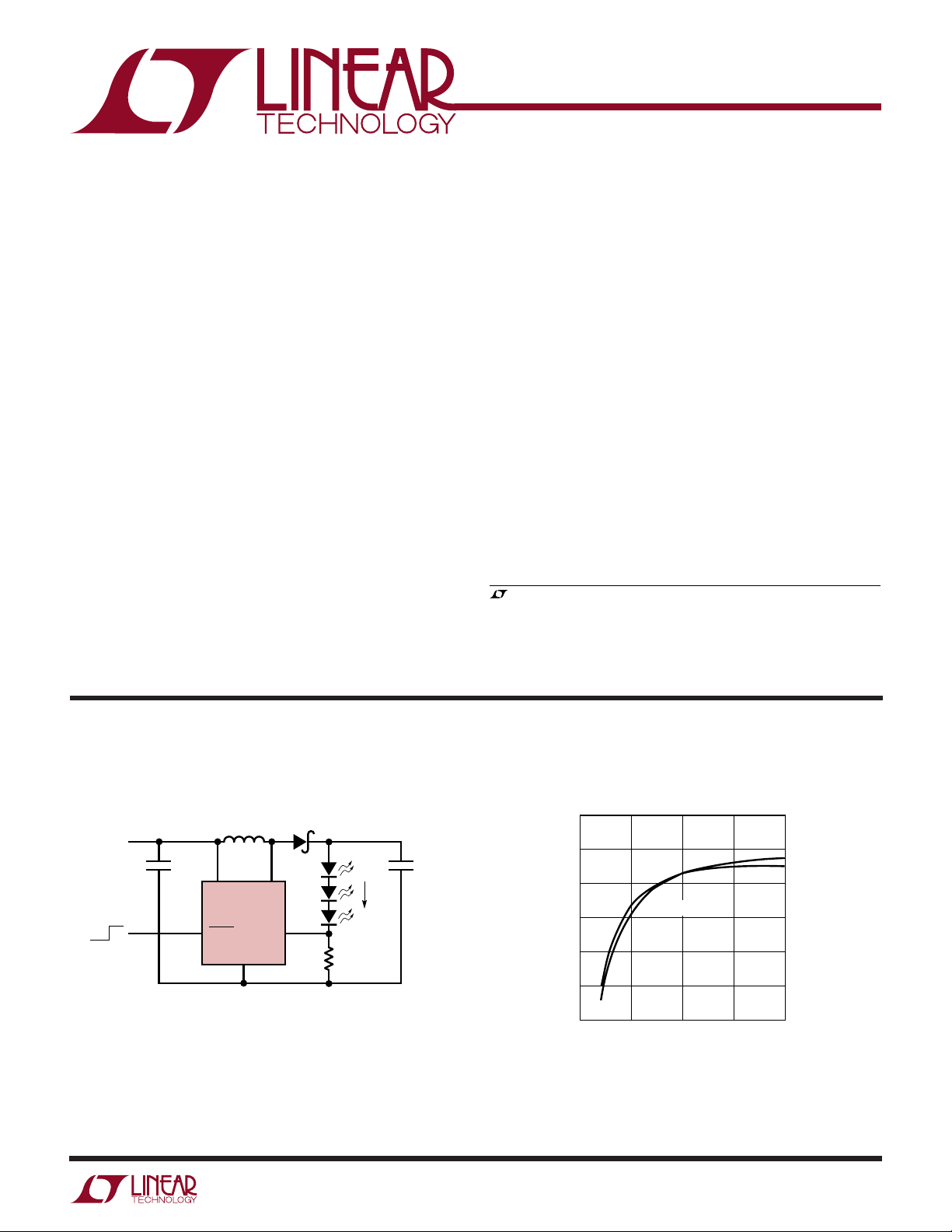
TYPICAL APPLICATIO
The LT®1937 is a step-up DC/DC converter specifically
designed to drive white LEDs with a constant current. The
device can drive two, three or four LEDs in series from a
Li-Ion cell. Series connection of the LEDs provides identical LED currents resulting in uniform brightness and
eliminating the need for ballast resistors. The LT1937
switches at 1.2MHz, allowing the use of tiny external
components. The output capacitor can be as small as
0.22µF, saving space and cost versus alternative solu-
tions. A low 95mV feedback voltage minimizes power loss
in the current setting resistor for better efficiency.
The LT1937 is available in low profile SC70 and ThinSOT
packages.
, LTC and LT are registered trademarks of Linear Technology Corporation.
ThinSOT is a trademark of Linear Technology Corporation.
V
3V TO 5V
OFF ON
L1
V
IN
SHDN
22µH
LT1937
GND
IN
C1
1µF
C1, C2: X5R OR X7R DIELECTRIC
D1: CENTRAL SEMICONDUCTOR CMDSH-3
L1: MURATA LQH3C-220 OR EQUIVALENT
SW
D1
LED 1
LED 2
LED 3
FB
15mA
R1
6.34Ω
Figure 1. Li-Ion Powered Driver for Three White LEDs
C2
0.22µF
1937 F01a
90
85
80
= 3V
V
IN
75
EFFICIENCY (%)
70
65
60
0
Conversion Efficiency
VIN = 3.6V
5101520
LED CURRENT (mA)
1937 TA01b
1937f
1
Page 2
LT1937
WWWU
ABSOLUTE AXI U RATI GS
(Note 1)
Input Voltage (VIN) ................................................. 10V
SW Voltage ............................................................. 36V
FB Voltage .............................................................. 10V
SHDN Voltage ......................................................... 10V
UU
W
PACKAGE/ORDER I FOR ATIO
ORDER PART
TOP VIEW
SW 1
GND 2
FB 3
S5 PACKAGE
5-LEAD PLASTIC TSOT-23
T
= 125°C, θJA = 256°C/ W IN FREE AIR
JMAX
= 120°C ON BOARD OVER GROUND PLANE
θ
JA
Consult LTC Marketing for parts specified with wider operating temperature ranges.
5 V
IN
4 SHDN
NUMBER
LT1937ES5
S5 PART MARKING
LTYN
Extended Commercial
Operating Temperature Range (Note 2)... –40°C to 85°C
Maximum Junction Temperature ..........................125°C
Storage Temperature Range ................. –65°C to 150°C
Lead Temperature (Soldering, 10 sec).................. 300°C
ORDER PART
TOP VIEW
SW 1
GND 2
FB 3
SC6 PACKAGE
6-LEAD PLASTIC SC70
T
= 125°C, θJA = 256°C/ W IN FREE AIR
JMAX
= 150°C ON BOARD OVER GROUND PLANE
θ
JA
6 V
IN
5 GND
4 SHDN
NUMBER
LT1937ESC6
SC6 PART MARKING
LAAB
ELECTRICAL CHARACTERISTICS
PARAMETER CONDITIONS MIN TYP MAX UNITS
Minimum Operating Voltage 2.5 V
Maximum Operating Voltage 10 V
Feedback Voltage ISW = 100mA, Duty Cycle = 66% 86 95 104 mV
FB Pin Bias Current 10 45 100 nA
Supply Current 1.9 2.5 mA
SHDN = 0V 0.1 1.0 µA
Switching Frequency 0.8 1.2 1.6 MHz
Maximum Duty Cycle 85 90 %
Switch Current Limit 320 mA
Switch V
CESAT
Switch Leakage Current VSW = 5V 0.01 5 µA
SHDN Voltage High 1.5 V
SHDN Voltage Low 0.4 V
SHDN Pin Bias Current 65 µA
Note 1: Absolute Maximum Ratings are those values beyond which the life
of the device may be impaired.
ISW = 250mA 350 mV
TA = 25°C, VIN = 3V, V
Note 2: The LT1937E is guaranteed to meet specifications from 0°C to
70°C. Specifications over the –40°C to 85°C operating temperature range
are assured by design, characterization and correlation with statistical
process controls.
= 3V, unless otherwise noted.
SHDN
2
1937f
Page 3
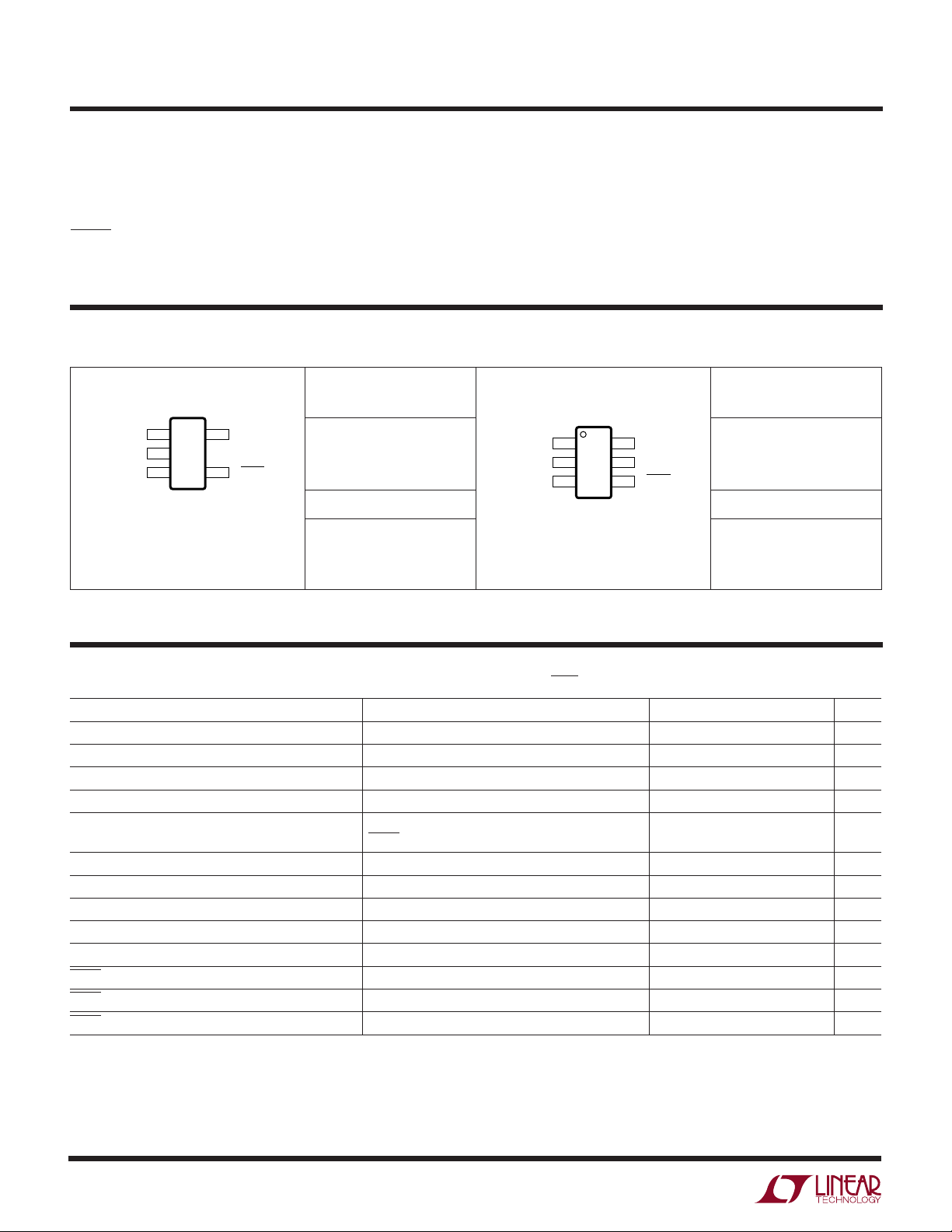
UW
TEMPERATURE (°C)
–50
0.8
1.0
1.4
25 75
1937 G03
0.6
0.4
–25 0
50 100
0.2
0
1.2
SWITCHING FREQUENCY (MHz)
DUTY CYCLE (%)
0
350
300
250
200
150
100
50
0
60
1937 G06
20 40 80 100
CURRENT LIMIT (mA)
TYPICAL PERFOR A CE CHARACTERISTICS
LT1937
Quiescent Current SHDN Pin Bias Current
2.2
2.0
1.8
1.6
1.4
1.2
(mA)
1.0
Q
I
0.8
0.6
0.4
0.2
0
2468
0
Feedback Bias Current
60
50
40
30
20
25°C
VIN (V)
–50°C
100°C
10
1937 G01
400
350
300
250
200
150
100
SHDN PIN BIAS CURRENT (µA)
50
0
–50
SHDN = 3.6V SHDN = 3V
SHDN = 2.7V
–25 0 50
TEMPERATURE (°C)
Efficiency vs Temperature
85
= 3.6V
V
IN
3 LEDs
84
83
82
EFFICIENCY (%)
I
LED
I
LED
I
LED
25
= 20mA
= 15mA
= 10mA
Switching Frequency
SHDN = 10V
75 100
1937 G02
Current Limit vs Duty Cycle
FEEDBACK BIAS CURRENT (nA)
10
0
–50
–25 0
U
PI FU CTIO S
SW (Pin 1): Switch Pin. Connect inductor/diode here.
Minimize trace area at this pin to reduce EMI.
GND (Pin 2): Ground Pin. Connect directly to local ground
plane.
FB (Pin 3): Feedback Pin. Reference voltage is 95mV.
Connect cathode of lowest LED and resistor here. Calculate resistor value according to the formula:
RFB = 95mV/I
50 100
25 75
TEMPERATURE (°C)
UU
LED
1937 G04
81
80
–50
0
TEMPERATURE (°C)
50
100
1937 G05
SHDN (Pin 4): Shutdown Pin. Connect to 1.5V or higher to
enable device; 0.4V or less to disable device.
GND (Pin 5, SC70 Package): Ground Pin. Connect to Pin
2 and to local ground plane
VIN (Pin 5/Pin 6 SC70 Package): Input Supply Pin. Must
be locally bypassed.
1937f
3
Page 4
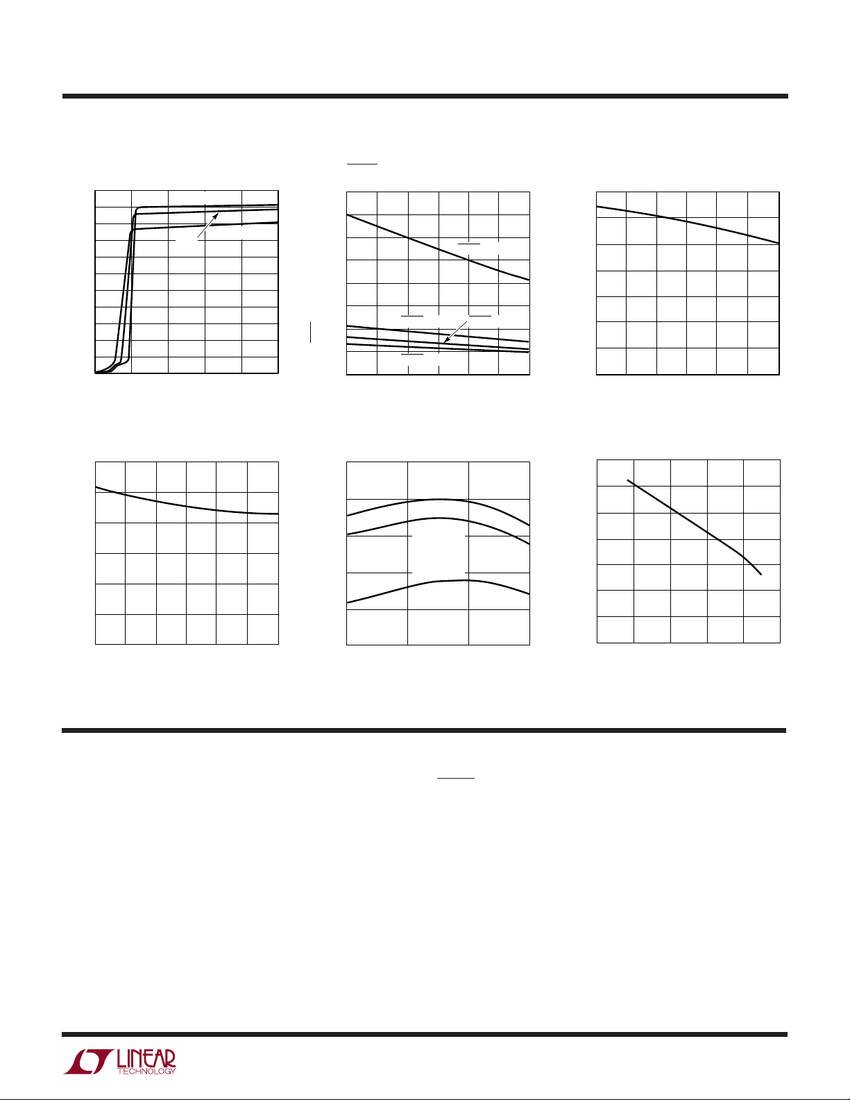
LT1937
BLOCK DIAGRA
W
(PIN 6 FOR
SC70 PACKAGE)
V
IN
5
FB
3
–
V
REF
1.25V
SHDN
4
95mV
SHUTDOWN
A1
+
R
C
C
C
Figure 2. LT1937 Block Diagram
U
OPERATIO
The LT1937 uses a constant frequency, current mode
control scheme to provide excellent line and load regulation. Operation can be best understood by referring to the
block diagram in Figure 2. At the start of each oscillator
cycle, the SR latch is set, which turns on the power switch
Q1. A voltage proportional to the switch current is added
to a stabilizing ramp and the resulting sum is fed into the
positive terminal of the PWM comparator A2. When this
voltage exceeds the level at the negative input of A2, the SR
latch is reset turning off the power switch. The level at the
negative input of A2 is set by the error amplifier A1, and is
simply an amplified version of the difference between the
feedback voltage and the reference voltage of 95mV. In
this manner, the error amplifier sets the correct peak
current level to keep the output in regulation. If the error
amplifier’s output increases, more current is delivered to
the output; if it decreases, less current is delivered.
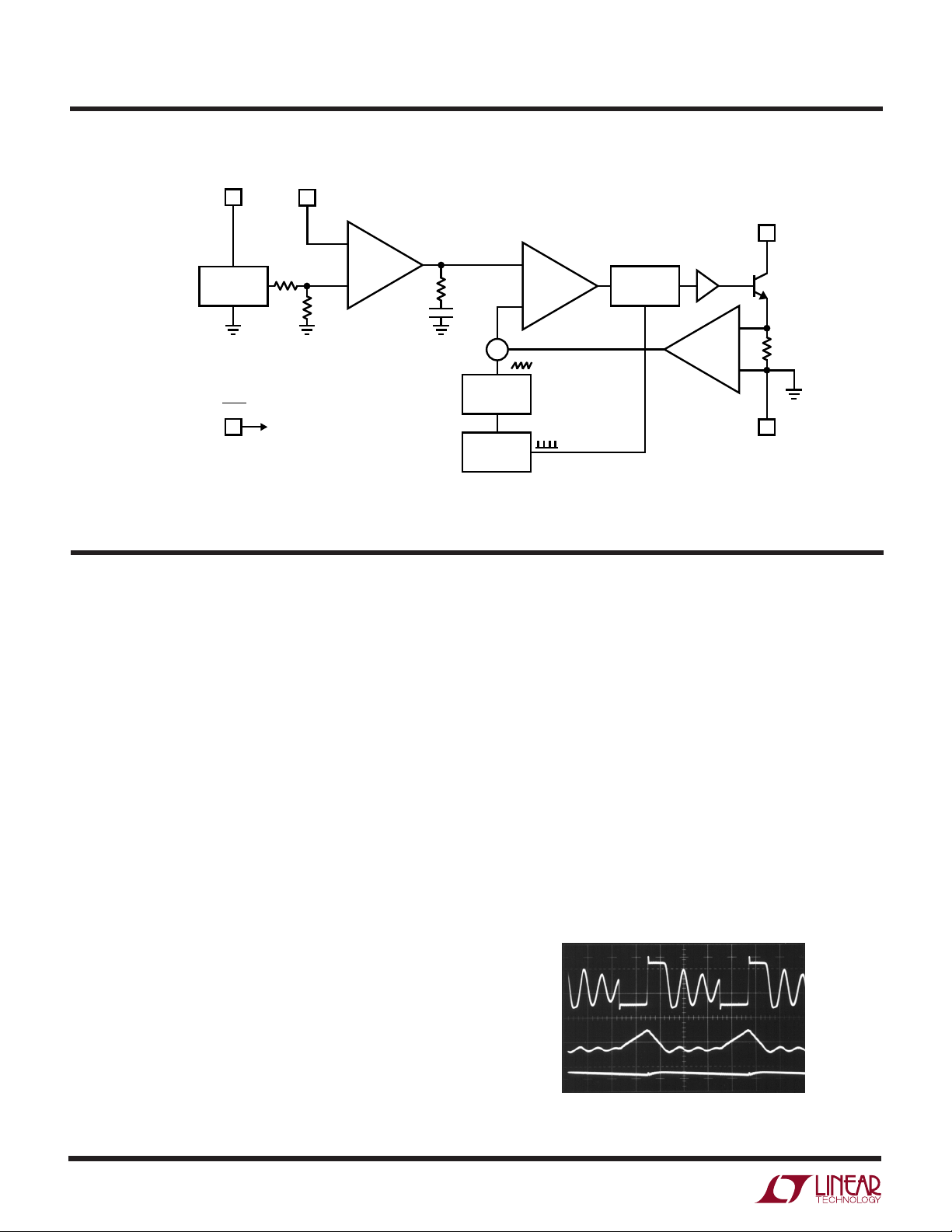
Minimum Output Current
The LT1937 can regulate three series LEDs connected at
low output currents, down to approximately 4mA from a
4.2V supply, without pulse skipping, using the same
external components as specified for 15mA operation. As
current is further reduced, the device will begin skipping
1
COMPARATOR
–
A2
+
RQ
S
DRIVER
SW
Q1
+
Σ
0.2Ω
–
RAMP
GENERATOR
1.2MHz
OSCILLATOR
(PINS 2 AND 5 FOR
SC70 PACKAGE)
2
GND
1937 BD1
pulses. This will result in some low frequency ripple,
although the LED current remains regulated on an average
basis down to zero. The photo in Figure 3 details circuit
operation driving three white LEDs at a 4mA load. Peak
inductor current is less than 50mA and the regulator
operates in discontinuous mode, meaning the inductor
current reaches zero during the discharge phase. After the
inductor current reaches zero, the switch pin exhibits
ringing due to the LC tank circuit formed by the inductor
in combination with switch and diode capacitance. This
ringing is not harmful; far less spectral energy is contained
in the ringing than in the switch transitions. The ringing
can be damped by application of a 300Ω resistor across
the inductor, although this will degrade efficiency.
V
SW
5V/DIV
I
L2
50mA/DIV
V
OUT
100mV/DIV
0.2µs/DIV
Figure 3. Switching Waveforms at I
LED
1937 F03
= 4mA, VIN = 3.6V
1937f
4
Page 5

WUUU
APPLICATIO S I FOR ATIO
LT1937
Inductor Selection
A 22µH inductor is recommended for most LT1937 appli-
cations. Although small size and high efficiency are major
concerns, the inductor should have low core losses at
1.2MHz and low DCR (copper wire resistance). Some
inductors in this category with small size are listed in
Table␣ 1. The efficiency comparison of different inductors
is shown in Figure 4.
Table 1. Recommended Inductors
CURRENT
DCR RATING
PART NUMBER (Ω) (mA) MANUFACTURER
LQH3C220 0.71 250 Murata
814-237-1431
www.murata.com
ELJPC220KF 4.0 160 Panasonic
714-373-7334
www.panasonic.com
CDRH3D16-220 0.53 350 Sumida
847-956-0666
www.Sumida.com
LB2012B220M 1.7 75 Taiyo Yuden
408-573-4150
www.t-yuden.com
LEM2520-220 5.5 125 Taiyo Yuden
408-573-4150
www.t-yuden.com
90
VIN = 3.6V
3LEDs
85
80
75
70
65
EFFICIENCY (%)
60
55
50
0
Figure 4. Efficiency Comparison of Different Inductors
MURATA LQH3C-220
PANASONIC ELJPC220KF
SUMIDA CDRH3D16-220
TAIYO YUDEN LB2012B220M
TAIYO YUDEN LEM2520-220
4 8 12 20142 6 10 18
LOAD CURRENT (mA)
16
1937 F04
Capacitor Selection
The small size of ceramic capacitors makes them ideal for
LT1937 applications. X5R and X7R types are recommended because they retain their capacitance over wider
voltage and temperature ranges than other types such as
Y5V or Z5U. A 1µF input capacitor and a 0.22µF output
capacitor are sufficient for most LT1937 applications.
Table 2. Recommended Ceramic Capacitor Manufacturers
MANUFACTURER PHONE URL
Taiyo Yuden 408-573-4150 www.t-yuden.com
AVX 843-448-9411 www.avxcorp.com
Murata 814-237-1431 www.murata.com
Kemet 408-986-0424 www.kemet.com
Diode Selection
Schottky diodes, with their low forward voltage drop and
fast reverse recovery, are the ideal choices for LT1937
applications. The forward voltage drop of a Schottky diode
represents the conduction losses in the diode, while the
diode capacitance (CT or CD) represents the switching
losses. For diode selection, both forward voltage drop and
diode capacitance need to be considered. Schottky diodes
with higher current ratings usually have lower forward
voltage drop and larger diode capacitance, which can
cause significant switching losses at the 1.2MHz switching frequency of the LT1937. A Schottky diode rated at
100mA to 200mA is sufficient for most LT1937 applications. Some recommended Schottky diodes are listed in
Table 3.
Table 3. Recommended Schottky Diodes
FORWARD VOLTAGE DIODE
PART CURRENT DROP CAPACITANCE
NUMBER (mA) (V) (pF) MANUFACTURER
CMDSH-3 100 0.58 at 7.0 at Central
100mA 10V 631-435-1110
www.centralsemi.com
CMDSH2-3 200 0.49 at 15 at Central
200mA 10V 631-435-1110
www.centralsemi.com
BAT54 200 0.53 at 10 at Zetex
100mA 25V 631-543-7100
www.zetex.com
1937f
5
Page 6

LT1937
WUUU
APPLICATIO S I FOR ATIO
LED Current Control
The LED current is controlled by the feedback resistor (R1
in Figure 1). The feedback reference is 95mV. The LED
current is 95mV/R1. In order to have accurate LED current,
precision resistors are preferred (1% is recommended).
The formula and table for R1 selection are shown below.
R1 = 95mV/I
LED
Table 4. R1 Resistor Value Selection
I
(mA) R1 (Ω)
LED
5 19.1
10 9.53
12 7.87
15 6.34
20 4.75
(1)
Open-Circuit Protection
In the cases of output open circuit, when the LEDs are
disconnected from the circuit or the LEDs fail, the feedback voltage will be zero. The LT1937 will then switch at
a high duty cycle resulting in a high output voltage, which
may cause the SW pin voltage to exceed its maximum 36V
rating. A zener diode can be used at the output to limit the
voltage on the SW pin (Figure 5). The zener voltage should
be larger than the maximum forward voltage of the LED
string. The current rating of the zener should be larger than
0.1mA.
L
V
IN
SHDN
22µH
LT1937
GND
V
IN
C
1µF
IN
SW
D
C
OUT
0.22µF
R2
FB
1k
R1
6.34Ω
Dimming Control
There are four different types of dimming control circuits:
1. Using a PWM Signal to SHDN Pin
With the PWM signal applied to the SHDN pin, the LT1937
is turned on or off by the PWM signal. The LEDs operate
at either zero or full current. The average LED current
increases proportionally with the duty cycle of the PWM
signal. A 0% duty cycle will turn off the LT1937 and
corresponds to zero LED current. A 100% duty cycle
corresponds to full current. The typical frequency range of
the PWM signal is 1kHz to 10kHz. The magnitude of the
PWM signal should be higher than the minimum SHDN
voltage high. The switching waveforms of the SHDN pin
PWM control are shown in Figures 6a and 6b.
LT1937
SHDN
PWM
FB
100mV/DIV
SHDN
2V/DIV
200µs/DIV 1937 F06a
(6a) 1kHz
FB
100mV/DIV
SHDN
2V/DIV
6
1937 F05
Figure 5. LED Driver with Open-Circuit Protection
20µs/DIV 1937 F06b
(6b) 10kHz
Figure 6. PWM Dimming Control Using the SHDN Pin
1937f
Page 7

WUUU
APPLICATIO S I FOR ATIO
LT1937
2. Using a DC Voltage
For some applications, the preferred method of brightness
control is a variable DC voltage to adjust the LED current.
The dimming control using a DC voltage is shown in
Figure␣ 7. As the DC voltage increases, the voltage drop on
R2 increases and the voltage drop on R1 decreases. Thus,
the LED current decreases. The selection of R2 and R3 will
make the current from the variable DC source much
smaller than the LED current and much larger than the FB
pin bias current. For VDC range from 0V to 2V, the selection
of resistors in Figure 7 gives dimming control of LED
current from 0mA to 15mA.
3. Using a Filtered PWM Signal
The filtered PWM signal can be considered as an adjust-
able DC voltage. It can be used to replace the variable DC
voltage source in dimming control. The circuit is shown in
Figure 8.
4. Using a Logic Signal
For applications that need to adjust the LED current in
discrete steps, a logic signal can be used as shown in
Figure 9. R1 sets the minimum LED current (when the
NMOS is off). R
sets how much the LED current
INC
increases when the NMOS is turned on. The selection of
R1 and R
follows formula (1) and Table 4.
INC
Start-up and Inrush Current
To achieve minimum start-up delay, no internal soft-start
circuit is included in LT1937. When first turned on without
an external soft-start circuit, inrush current is about 200mA
as shown in Figure␣ 10. If soft-start is desired, the recommended circuit and the waveforms are shown in Figure 11.
If both soft-start and dimming are used, a 10kHz PWM
signal on SHDN is not recommended. Use a lower frequency or implement dimming through the FB pin as
shown in Figures 7, 8 or 9.
LT1937
FB
R3
90k
V
DC
R2
5k
R1
6.3Ω
1937 F07
Figure 7. Dimming Control Using a DC Voltage
LT1937
FB
R2
5k
R1
6.3Ω
1937 F08
PWM
10k
R3
90k
0.1µF
Figure 8. Dimming Control Using a Filtered PWM Signal
LT1937
FB
R
INC
LOGIC
SIGNAL
2N7002
R1
1937 F09
Figure 9. Dimming Control Using a Logic Signal
I
IN
100mA/DIV
FB
100mV/DIV
SHDN
2V/DIV
VIN = 3.6V 50µs/DIV 1937 F09
THREE LEDs
15mA
Figure 10. Start-Up Waveforms Without Soft-Startup Circuit
1937f
7
Page 8

LT1937
16
5
4
R1
2
3
R2
R3
DIMMING
CONTROL
C
O
C
IN
V
IN
GND
SHDN
1937 F12b
D
L
WUUU
APPLICATIO S I FOR ATIO
D1
2.2nF
R2
LT1937
D2: MMBT
D2
FB
1k
5k
R1
6.34Ω
C
OUT
1937 F11a
I
100mA/DIV
FB
100mV/DIV
SHDN
2V/DIV
IN
VIN = 3.6V 50µs/DIV 1937 F11b
THREE LEDs
15mA
(11a) Recommended Soft-Startup Circuit
Figure 11. Recommended Soft-Startup Circuit and Waveforms
Board Layout Consideration
As with all switching regulators, careful attention must be
paid to the PCB board layout and component placement.
To maximize efficiency, switch rise and fall times are made
as short as possible. To prevent electromagnetic interference (EMI) problems, proper layout of the high frequency
switching path is essential. The voltage signal of the SW
pin has sharp rise and fall edges. Minimize the length and
D
C
O
R2
L
15
2
3
R1
4
V
IN
C
IN
GND
SHDN
(11b) Soft-Startup Waveforms
area of all traces connected to the SW pin and always use
a ground plane under the switching regulator to minimize
interplane coupling. In addition, the ground connection for
the feedback resistor R1 should be tied directly to the GND
pin and not shared with any other component, ensuring a
clean, noise-free connection. Recommended component
placement is shown in Figure 12.
8
1937 F12a
(SC70 Package)
1937f
DIMMING
CONTROL
R3
(SOT-23 Package)
Figure 12. Recommended Component Placement
Page 9

U
TYPICAL APPLICATIO S
Li-Ion to Two White LEDs Two LED Efficiency
LT1937
3V TO 5V
V
3V TO 5V
V
IN
C
1µF
C
: TAIYO YUDEN JMK107BJ105
IN
C
OUT
D: CENTRAL CMDSH2-3
L: MURATA LQH3C220
IN
C
IN
1µF
22µH
IN
V
IN
LT1937
SHDN
: AVX 0603ZD105
GND
L
SW
FB
D
V
DC
DIMMING
90k
C
OUT
1µF
5k
R1
2Ω
1937 TA05a
86
84
82
80
78
76
EFFICIENCY (%)
74
72
70
0
VIN = 3V
10
20
LED CURRENT (mA)
VIN = 3.6V
Li-Ion to Three White LEDs Three LED Efficiency
90
85
80
= 3V
V
IN
75
EFFICIENCY (%)
70
65
VIN = 3.6V
V
IN
SHDN
L
22µH
LT1937
GND
SW
FB
D
V
DC
DIMMING
90k
C
OUT
0.22µF
5k
R1
4Ω
30
40
1937 TA05a
C
: TAIYO YUDEN JMK107BJ105
IN
C
: AVX 0603YD224
OUT
D: CENTRAL CMDSH-3
L: MURATA LQH3C220
1937 TA01a
60
0
5101520
LED CURRENT (mA)
1937 TA01b
1937f
9
Page 10

LT1937
U
U
TYPICAL APPLICATIO S
TYPICAL APPLICATIO S
Li-Ion to Five White LEDs Five LED Efficiency
V
3V TO 5V
V
IN
5V
IN
C
IN
1µF
C
: TAIYO YUDEN JMK107BJ105
IN
: TAIYO YUDEN GMK212BJ224
C
OUT
D: CENTRAL CMDSH-3
L: MURATA LQH3C220
5V to Seven White LEDs
C
IN
1µF
V
IN
SHDN
C
: TAIYO YUDEN JMK107BJ105
IN
: TAIYO YUDEN GMK212BJ224
C
OUT
D: CENTRAL CMDSH-3
L: MURATA LQH3C220
V
IN
SHDN
L
22µH
LT1937
GND
L
22µH
LT1937
GND
SW
FB
DIMMING
SW
FB
V
DC
DIMMING
D
V
90k
D
C
OUT
DC
90k
5k
R1
4Ω
0.22µF
1937 TA03a
85
80
VIN = 3V
75
EFFICIENCY (%)
70
65
0
VIN = 3.6V
2468
LOAD CURRENT (mA)
10 12
1937 TA03b
Seven LED Efficiency
85
C
OUT
0.22µF
5k
R1
4Ω
1937 TA04a
80
75
EFFICIENCY (%)
70
65
0
510
LOAD CURRENT (mA)
15
1937 TA04b
10
1937f
Page 11

PACKAGE DESCRIPTIO
0.62
MAX
3.85 MAX
2.62 REF
U
S5 Package
5-Lead Plastic TSOT-23
(Reference LTC DWG # 05-08-1635)
0.95
REF
1.22 REF
1.50 – 1.75
1.4 MIN
2.80 BSC
(NOTE 4)
PIN ONE
2.90 BSC
(NOTE 4)
LT1937
RECOMMENDED SOLDER PAD LAYOUT
PER IPC CALCULATOR
0.20 BSC
DATUM ‘A’
0.30 – 0.50 REF
NOTE:
1. DIMENSIONS ARE IN MILLIMETERS
2. DRAWING NOT TO SCALE
3. DIMENSIONS ARE INCLUSIVE OF PLATING
4. DIMENSIONS ARE EXCLUSIVE OF MOLD FLASH AND METAL BURR
5. MOLD FLASH SHALL NOT EXCEED 0.254mm
6. JEDEC PACKAGE REFERENCE IS MO-193
0.09 – 0.20
(NOTE 3)
(Reference LTC DWG # 05-08-1638)
3.26 MAX
2.1 REF
0.47
MAX
0.65
REF
1.16 REF
0.96 MIN
0.95 BSC
0.80 – 0.90
1.00 MAX
SC6 Package
6-Lead Plastic SC70
1.15 – 1.35
1.80 – 2.40
(NOTE 4)
1.90 BSC
1.80 – 2.20
(NOTE 4)
INDEX AREA
(NOTE 6)
0.30 – 0.45 TYP
5 PLCS (NOTE 3)
0.01 – 0.10
S5 TSOT-23 0302
RECOMMENDED SOLDER PAD LAYOUT
0.10 – 0.40
NOTE:
1. DIMENSIONS ARE IN MILLIMETERS
2. DRAWING NOT TO SCALE
3. DIMENSIONS ARE INCLUSIVE OF PLATING
4. DIMENSIONS ARE EXCLUSIVE OF MOLD FLASH AND METAL BURR
PER IPC CALCULATOR
0.10 – 0.30
0.10 – 0.18
(NOTE 3)
Information furnished by Linear Technology Corporation is believed to be accurate and reliable.
However, no responsibility is assumed for its use. Linear Technology Corporation makes no representation that the interconnection of its circuits as described herein will not infringe on existing patent rights.
PIN 1
0.65 BSC
0.80 – 1.00
1.00 MAX
5. MOLD FLASH SHALL NOT EXCEED 0.254mm
6. DETAILS OF THE PIN 1 INDENTIFIER ARE OPTIONAL,
BUT MUST BE LOCATED WITHIN THE INDEX AREA
7. EIAJ PACKAGE REFERENCE IS EIAJ SC-70
0.15 – 0.30
6 PLCS (NOTE 3)
0.00 – 0.10
SC6 SC70 0302
1937f
11
Page 12

LT1937
TYPICAL APPLICATIO
3V TO 5V
Four LED Efficiency
85
80
VIN = 3V
75
EFFICIENCY (%)
70
60
0
= 3.6V
V
IN
510
LOAD CURRENT (mA)
U
V
IN
C
IN
C
OUT
D: CENTRAL CMDSH-3
L: MURATA LQH3C220
15 20
1937 TA02b
Li-Ion to Four White LEDs
L
22µH
C
IN
1µF
DIMMING
V
IN
SHDN
: TAIYO YUDEN JMK107BJ105
: AVX 0603YD224
SW
LT1937
FB
GND
D
V
DC
90k
10V/DIV
100mA/DIV
100mV/DIV
5k
V
SW
I
SW
V
OUT
R1
4Ω
= 3.6V
V
IN
FOUR LEDs
15mA
C
OUT
0.22µF
1937 TA02a
Switching Waveforms
0.2µs/DIV
1937 TA02c
RELATED PARTS
PART NUMBER DESCRIPTION COMMENTS
LT1615 Micropower Step-Up Converter in ThinSOT Up to 36V Output; 20µA IQ, VIN: 1V to 15V,
Can Drive Up to Six LEDs, ThinSOT Package
LT1618 Constant Current/Voltage Step-Up DC/DC 1.4MHz, Drives Up to 20 LEDs, MS10 Package
LT1932 White LED Step-Up Converter in ThinSOT 1.2MHz, VIN = 1V to 10V, Drives Up to Eight LEDs from 3V Input,
ThinSOT Package
LT1944/LT1944-1 Dual Micropower Step-Up Converter VIN = 1.2V to 15V, Two Independent DC/DCs, Up to 36V
MS10 Package
LTC®3200/LTC3200-5 Low Noise White LED Charge Pump Converter 2MHz, 100mA, No Inductor Required, MS8/ThinSOT Packages
For up to 6 LEDs
LTC3201 Ultralow Noise White LED Charge Pump Converter 1.8MHz, 100mA, No Inductor Required, DAC Brightness Adj,
For up to 6 LEDs MS8 Package
LTC3202 Low Noise White LED Fractional Charge Pump Converter 1.5MHz, 125mA, No Inductor Required, Digital Brightness Adjust,
For up to 6 LEDs MS8 Package
LT/TP 0702 2K • PRINTED IN USA
12
Linear Technology Corporation
1630 McCarthy Blvd., Milpitas, CA 95035-7417
(408) 432-1900 ● FAX: (408) 434-0507
●
www.linear.com
LINEAR TECHNOLOGY CORPORATION 2002
, 20µA IQ,
OUT
1937f
Page 13

 Loading...