

Page 1

DEMO MANUAL DC194
MICROPOWER BOOST REGULATOR
LT1317/LT1317B
Micropower, 600kHz
U
PWM DC/DC Converters
DESCRIPTIO
Demonstration Circuit DC194 is a micropower boost
regulator that converts an input as low as 1.5V to an output
of 3.3V or 5.0V. DC194 version A uses the LT®1317CMS8;
version B uses the LT1317BCMS8. This circuit provides
regulated power for battery-powered devices, such as
laptop and palmtop computers, cellular phones, pagers,
LCD panels and other portable devices. It is also useful for
local conversion of logic supplies, such as 3.3V to 5V
conversion in PC card devices.
The LT1317 and LT1317B are 600kHz PWM DC/DC converters. Their high operating frequency and small package
result in small, cost effective solutions. The micropower
LT1317 shifts automatically to low power Burst Mode
operation at light loads, whereas the LT1317B operates at
a fixed frequency at all loads. Both parts feature a lowbattery detector that remains active while the part is shut
down. The wide voltage ratings (12V input and 30V
switch) make the LT1317 and LT1317B versatile parts,
suitable for implementing boost, flyback and SEPIC
topologies.
, LTC and LT are registered trademarks of Linear Technology Corporation.
Burst Mode is a trademark of Linear Technology Corportion.
UWWW
PERFOR A CE SU ARY
PARAMETER CONDITIONS VALUE
Input Voltage (Note 1) V
Maximum Load Current, Min V
Shutdown Current, Typ VIN = 2.5V, SHDN = 0V 25µA
No Load Quiescent Current, Typ V
Note 1: This limit is based on the DC194 circuit. The LT1317 can operate
from high supply voltages.
= 3.3V 1.5V to 3.6V
OUT
V
= 5V 1.5V to 5.3V
OUT
= 3.3V, VIN = 1.6V 175mA
OUT
= 3.3V, VIN = 2.4V 320mA
V
OUT
= 5V, VIN = 2V 140mA
V
OUT
= 5V, VIN = 3.3V 290mA
V
OUT
= 3.3V, VIN = 2.4V, LT1317 125µA
OUT
= 3.3V, VIN = 2.4V, LT1317B 4.8mA
V
OUT
TM
U
W
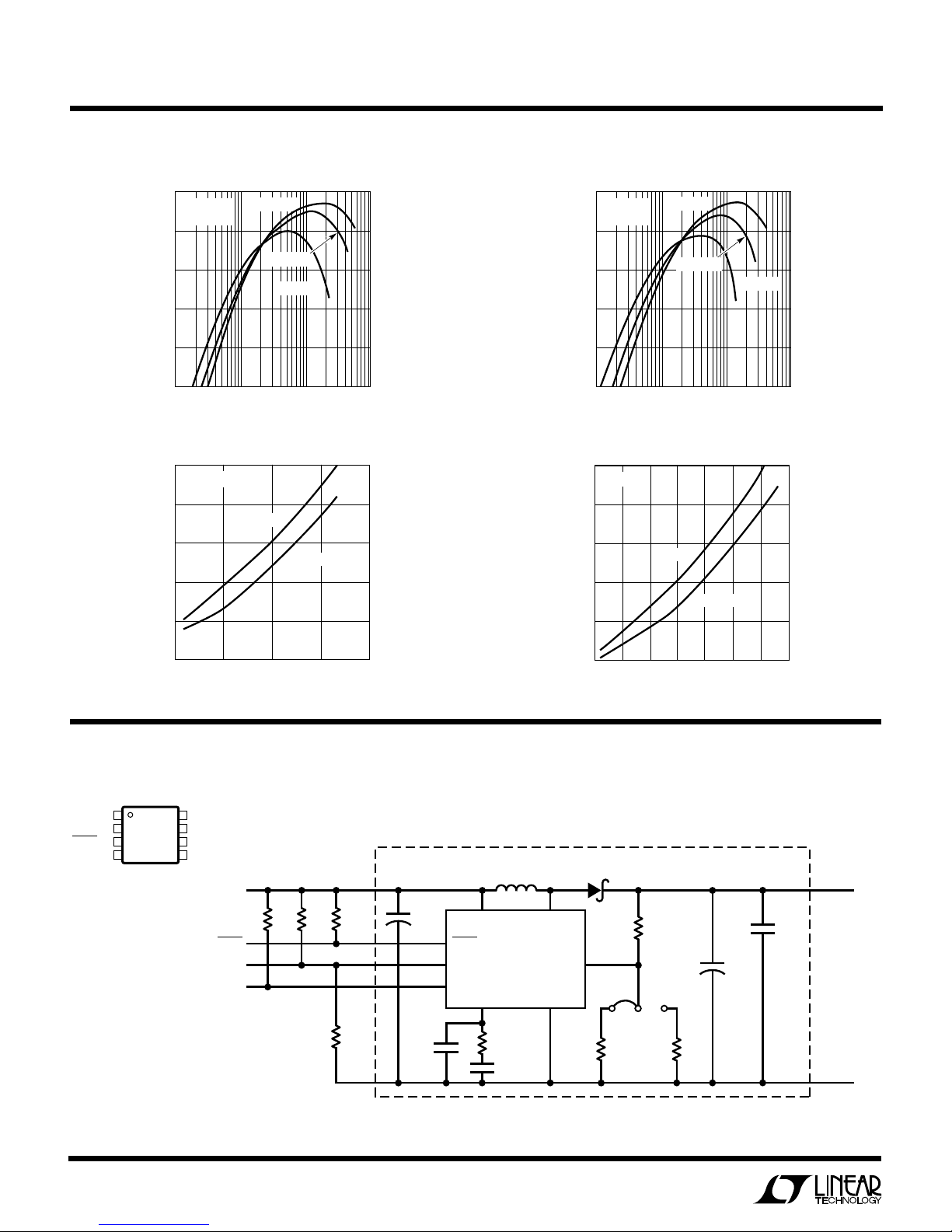
TYPICAL PERFOR A CE CHARACTERISTICS A D BOARD PHOTO
LT1317 Efficiency
90
VIN = 3V
80
LT1317
V
OUT
VIN = 1.6V
= 3.3V
1
LOAD CURRENT (mA)
70
60
EFFICIENCY (%)
50
40
0.3 10 100 1000
VIN = 2.4V
DC194 G04
LT1317 Efficiency
90
80
70
60
EFFICIENCY (%)
50
LT1317
= 5V
V
OUT
40
0.3 10 100 1000
1
VIN = 3.3V
VIN = 2.4V
VIN = 1.6V
LOAD CURRENT (mA)
U
Board Photo
DC194 BP
DC194 G03
1
Page 2
DEMO MANUAL DC194
LOAD CURRENT (mA)
1
EFFICIENCY (%)
90
80
70
60
50
40
10 100 1000
DC194 G05
LT1317B
V
OUT
= 5V
VIN = 3.3V
VIN = 1.6V
VIN = 2.4V
MICROPOWER BOOST REGULATOR
UW
TYPICAL PERFORMANCE CHARACTERISTICS
LT1317B Efficiency
90
LT1317B
V
OUT
80
70
60
EFFICIENCY (%)
50
40
1
= 3.3V
VIN = 3V
VIN = 2.4V
VIN = 1.6V
10 100 1000
LOAD CURRENT (mA)
Load Current vs Input Voltage
600
V
= 3.3V
OUT
500
400
300
OUTPUT CURRENT (mA)
200
TYPICAL
MINIMUM
DC194 G06
LT1317B Efficiency
Load Current vs Input Voltage
600
V
= 5V
OUT
500
400
300
OUTPUT CURRENT (mA)
200
TYPICAL
MINIMUM
100
1.5
2.0
2.5
INPUT VOLTAGE (V)
3.0
3.5
DC194 G01
W UW
PACKAGE A D SCHE ATIC DIAGRA SM
TOP VIEW
V
1
C
2
FB
3
SHDN
4
GND
MS8 PACKAGE
8-LEAD PLASTIC MSOP
NOTES:
1. FOR VERSION A: USE LT1317CMS8 (LTHA)
2. FOR VERSION B; USE LT1317BCMS8 (LTHB)
3. FOR 3.3V OUTPUT, INSTALL SHUNT AT
JP1 PINS 1, 2
FOR 5V OUTPUT, INSTALL SHUNT AT
JP1 PINS 2, 3
8
LBO
7
LBI
6
V
IN
5
SW
SHDN
LBO
LT1317CMS8
LT1317BCMS8
V
IN
R7
OPT
LBI
R6
OPT
L1
10µH
R4
OPT
R5
OPT
+
C1
22µF
10V
3
7
8
C5
100pF
6
V
IN
LT1317CMS8(A)
SHDN
LBI
LT1317BCMS8(B)
LBO
V
C
1
R3
33k
C3
3300pF
LTHA
LTHB
Figure 1. Demo Board Schematic
U1
OR
SW
GND
5
4
100
1.5
MBR0520LT1
2
FB
3.0
R1B
332k
5V
3.5
4.0
C2
+
100µF
6.3V
2.5
2.0
INPUT VOLTAGE (V)
D1
R2
1.00M
3.3V
5V
231
JP1
R1A
604k
3.3V
4.5
DC194 G02
5.0
C4
0.1µF
DC194 F01
V
GND
OUT
2
Page 3
DEMO MANUAL DC194
MICROPOWER BOOST REGULATOR
PARTS LIST
REFERENCE
DESIGNATOR QUANTITY PART NUMBER DESCRIPTION VENDOR TELEPHONE
C1 1 TPSB226M010R0700 22µF 10V 20% Tantalum Capacitor AVX (207) 282-5111
C2 1 TPSC107M006R0150 100µF 6.3V 20% Tantalum Capacitor AVX (207) 282-5111
C3 1 0805YG332KAT2 3300pF 16V Y5V 0805 Capacitor AVX (843) 946-0362
C4 1 08053G104KAT2 0.1µF 25V Y5V 0805 Capacitor AVX (843) 946-0362
C5 1 0805YG101KAT2 100pF 16V Y5V 0805 Capacitor AVX (843) 946-0362
D1 1 MBR0520LT1 20V 0.5A SOD123 Schottky Diode Motorola (800) 441-2447
L1 1 CD43-100MC 10µH CD43 Inductor Sumida (847) 956-0666
R1A 1 CR10-6043F-T 604k 1/10W 1% 0805 Resistor TAD (800) 508-1521
R1B 1 CR10-3323F-T 332k 1/10W 1% 0805 Resistor TAD (800) 508-1521
R2 1 CR10-1004F-T 1M 1/10W 1% 0805 Resistor TAD (800) 508-1521
R3 1 CR10-333J-T 33k 1/8W 5% 0805 Resistor TAD (800) 508-1521
R4 (Optional) 1 CR18-104J-T 100k 1/8W 5% 1206 Resistor TAD (714) 255-9123
R5 to R7 (Optional) 3 CR18-XXXJ-T XXX 1/8W 5% 1206 Resistor TAD (714) 255-9123
JP1 1 3801S-03-G1 3-Pin Header, 0.1" Center Comm (626) 301-4200
1 CCIJ230-G SHUNT FOR JP1 Comm (626) 301-4200
U1 1 LT1317CMS8, MSOP LTHA DC/DC Converter Version A LTC (408) 432-1900
LT1317BCMS8, MSOP LTHB DC/DC Converter Version B
QUICK START GUIDE
DC194 can regulate a 3.3V output from an input of 1.5V
to 3.6V; it can regulate a 5V output from an input of 1.5V
to 5.3V. Select the desired output voltage by moving
jumper JP1 to the appropriate position. Apply the DC
input voltage between the VIN and GND terminals of the
DC194. Do not apply more than 5.5V to the input of this
circuit.
With the input supply present, the LT1317/LT1317B will
regulate the output to 3.3V or 5V. Attach a suitable load
between V
and GND.
OUT
The LT1317/LT1317B can be placed in shutdown mode
by tying the SHDN terminal to the GND terminal. For
normal operation, the SHDN terminal can be left floating
or pulled high (above 1.4V and up to VIN).
Note that, as with any boost regulator, there is a direct DC
path between the input and output; a shorted output will
draw large currents, possibly damaging the DC194.
3
Page 4
DEMO MANUAL DC194
MICROPOWER BOOST REGULATOR
U
OPERATIO
INTRODUCTION
The LT1317 and LT1317B are 600kHz PWM step-up
DC/DC converters. With a wide input voltage range (1.5V
to 12V) and high switch voltage (30V), these parts are
suitable for a wide variety of switching regulator circuits.
DC194 demonstrates their application in a simple boost
regulator with an output of either 3.3V or 5V.
DC194 is available in two versions. Version A uses the
LT1317CMS8. At light loads, this part switches automatically into power-saving Burst Mode operation, resulting in
high efficiency over a broad range of load currents. Version B uses the LT1317BCMS8, which operates at a fixed
frequency, regardless of load, eliminating low frequency
ripple on the output at the expense of light load efficiency.
You can confirm which version of the board you have by
checking the code on the IC; the LT1317 is marked with the
code LTHA, whereas the LT1317B is marked with LTHB. In
the comments below, “LT1317” will refer to both parts. In
cases where their characteristics result in different behavior, the LT1317B will be mentioned explicitly.
This manual describes the operation of this demonstration
circuit, its performance and variations on the basic circuit.
For a thorough discussion of the LT1317 and its application, please consult the part’s data sheet.
Hookup and Initial Tests
Select the desired output voltage by moving jumper JP1.
The input can safely accept a voltage up to 5.5V. A good
starting point is to apply 2.5V between the VIN and GND
terminals of the DC194, using a bench-top supply with a
1A current limit. Because the SHDN pin of the LT1317 has
been left floating, the LT1317 will begin operating as soon
as VIN is above 1.5V.
A load can be applied between the V
and GND termi-
OUT
nals, using either a fixed resistor, a decade resistor box
(provided that it is rated for the power) or an active load.
A simple initial load might be a 1/2W 100Ω resistor.
Warning: Because the basic boost circuit contains a DC
path between the input and output (through inductor L1
and diode D1), the circuit is not protected against a
shorted output. It is recommended that preliminary testing of the circuit be performed using a current-limited
supply on the input.
With power applied to the DC194, the LT1317 should be
switching and regulating the output. Figure 3 shows some
of the circuit’s operating waveforms. The scope photos
show the output voltage, the current through inductor L1
and the voltage on the SW pin of the LT1317. The LT1317
is in Burst Mode operation in the first photo. The second
photo shows operation at a higher load current, where the
LT1317 is operating at a fixed frequency. LT1317B circuits
will operate in this mode at all load currents.
DC194 is a fairly simple low power switching regulator.
However, some precautions are necessary in order to test
the circuit safely. Proper hookup and accurate measurements are necessary for meaningful evaluation of efficiency and line and load regulation. Refer to Figure 2 for
proper connections.
I
OUT
A
V
V
OUT
BENCH
SUPPLY
1.5V TO 5.5V
1A
Figure 2. Recommended Hookup for Proper Evaluation
of Efficiency and Regulation (See Text)
A
C
BULK
+
I
IN
V
V
IN
4
V
OUT
GND
V
IN
DC194
DC194 F02
PERFORMANCE
Input Range and Power Capability
The LT1317 will operate from inputs above 1.5V. The
maximum allowable input voltage to this circuit is 5.5V,
which is based on the voltage ratings of the input and
output capacitors C1 and C2. The boost circuit will allow
the LT1317 to regulate the output only when the input
voltage is less than the desired output voltage plus one
diode drop. This means that the practical input range is
1.5V to 3.6V for a 3.3V output and 1.5V to 5.3V for a 5V
output.
The power capability of the DC194 is determined primarily
by the input voltage and the current limit of the LT1317’s
internal power switch and, to a lesser extent, by the value
of inductor L1. Therefore, the maximum load current that
this circuit can supply depends on the input voltage. A
Page 5

OPERATIO
V
OUT
AC COUPLED
100mV/DIV
I
L1
200mA/DIV
V
SW
5V/DIV
V
OUT
AC COUPLED
100mV/DIV
I
L1
200mA/DIV
V
SW
5V/DIV
U
5µs/DIV
DC194 F03a
DEMO MANUAL DC194
MICROPOWER BOOST REGULATOR
LT1317 will run in this condition. The LT1317 will also
operate if this pin is pulled above 1.4V by an external
signal. The SHDN pin can be pulled as high as VIN + 0.3V.
The LT1317 is placed in shutdown mode by pulling this pin
below 0.4V; you can do this by tying the SHDN terminal of
the DC194 to the GND terminal. The current consumption
of the LT1317 in shutdown mode is typically 25µ A. However, the load can draw additional current through the
inductor and catch diode, raising the power consumption
in shutdown. The LT1317’s low-battery detector remains
active in shutdown. Applications of the low-battery detector are discussed below.
Efficiency
The efficiency of the DC194 is plotted in the Typical
Performance section of this manual. Efficiency measurements should be made with care, as there is plenty of
opportunity for errors to creep in.
1µs/DIV
DC194 F03b
Figure 3. DC194’s Operating Waveforms. In the Upper Photo,
the LT1317 Is in Burst Mode, Delivering 50mA to the Load. In
the Lower Photo, the Load Curent Is 160mA and the LT1317 Is
Switching at 600kHz. VIN = 2.5V, V
OUT
= 3.3V
graph of maximum load appears in the Typical Performance section of this manual. The lower curve shows the
guaranteed load capability based on the minimum current
limit specification in the LT1317 data sheet. The upper
curve shows the load capability of a typical DC194. As load
current is increased beyond this level, the output voltage
will sag as the LT1317 reaches its current limit. Again, be
aware that L1 and D1 provide a direct path between the
input and output and that this circuit does not limit the
output current. As an increasing load drags the output
voltage below the input, a larger current will flow, limited
only by the impedance of the power source, inductor L1
and diode D1.
Shutdown Mode
The SHDN pin of the LT1317 is tied directly to the SHDN
terminal of the DC194 and has been left floating. An
internal current source will pull up on this pin and the
The efficiency is defined as the power delivered to the load
divided by the power drawn from the input supply. Normally, the average input voltage, input current, output
voltage and output current are measured under steadystate conditions and the efficiency is calculated from these
values. Each should be measured with the highest accuracy and precision possible.
Figure 2 shows connections for the proper measurement
of efficiency and output regulation. The input and output
voltages are measured at the DC194 in order to avoid
including voltage drops across ammeters and terminal
connections. It is best to take all of these measurements
at one time. Be aware that most digital multimeters drop
significant voltage when they are used as ammeters, so
you must measure the input voltage while the ammeter is
in the circuit—the input voltage will be lower than the
voltage at the output of your bench-top supply. Another
difficulty occurs at low power when the LT1317 is in Burst
Mode operation. Here, the part will be drawing a few
hundred milliamperes while switching, but only a few
hundred microamperes average. An ammeter set to a
sensitive scale will have too much resistance to allow
these pulses of current to pass without large voltage
drops. The result is that the power delivered to the LT1317
is not equal to the average current times the average
5
Page 6

DEMO MANUAL DC194
MICROPOWER BOOST REGULATOR
U
OPERATIO
voltage. Normally, the high resistance of the ammeter will
not be present, so its negative effect on efficiency measurements is misleading. This measurement problem can
be avoided by adding a large (1000µ F to 10,000µ F) bypass
capacitor across VIN between the ammeter and the DC194.
Comments on Layout
The layout used for this demonstration circuit may be
transferred to your circuit board (Gerber files are available). Also, the data sheet includes layout guidelines.
A boost regulator contains a high frequency current loop
that includes the power switch (between the SW and GND
pins of the LT1317), the diode (D1) and the output
capacitor (C2). This loop should be kept small and an
unbroken ground plane should be placed below it. Connect this local ground plane to the LT1317 near its ground
pin and to the system ground at just one point. The
feedback resistors and the components on the VC pin
should be as close as possible to the LT1317 and should
be returned to the LT1317’s ground pin.
Testing in Your System
You may want to paste this circuit into your system to test
compatibility. This should be done with care, since long
hookup wires and ground loops can introduce noise
sources and regulation problems that would not be present
if the LT1317 DC/DC converter was properly designed into
your PCB.
Treat the DC194 as a 3-terminal device with VIN, V
GND terminals. Wire the DC194 to your circuit board with
wires as short as practical, to points on the circuit board
that are close to each other. Also, add high frequency
bypass capacitors (0.1µ F ceramics) from VIN and V
ground on your circuit board.
If you are bringing power directly to the DC194, use two
wires from the input source to the VIN and GND terminals
of the DC194. The output power should be applied to your
system as described above, and either the input supply or
your circuit should be floating in order to avoid ground
loops.
OUT
OUT
and
to
DESIGN ALTERNATIVES
Component Selection
The components used for the DC194 represent a compromise in cost, performance and size. They are well matched
for the power capabilities of the LT1317 but there are many
options for the designer to optimize the circuit for his or
her application.
Diode D1 (Motorola MBR0520LT1) is a 0.5A, 20V Schottky diode. It is a good choice for nearly any LT1317
application, unless the output voltage or the circuit topology requires a diode rated for higher reverse voltages.
Motorola also offers 30V and 40V versions. Most 0.5A and
1A Schottky diodes are suitable and they are available
from many manufacturers. If you use a silicon diode, it
must be an ultrafast recovery type. Efficiency will be lower
due to the silicon diode’s higher forward voltage drop.
L1 is a 10µ H inductor rated for 1A of operating current. The
value of the inductor should be matched to the power
requirements and operating voltages of your application.
In most cases a value of 10µH is suitable. The inductor
should be rated for ~0.75A peak without excessive saturation—the current limit of the LT1317 internal power
switch allows the part to tolerate moderate inductance
loss. The Sumida CD43-100 used on the DC194 has a
relatively small footprint with low losses. The DO1608
series from Coilcraft offers a similar inductor. A smaller,
less expensive choice is the Murata LQH3C100K24, which
fits in a tiny 1210 footprint. Efficiency will be slightly lower
at higher operating currents. Finally, Coiltronics’ CTX10-1
is a surface mount toroidal inductor with good performance; it will generate lower stray magnetic fields than the
drum-type inductors listed above.
Lower Ripple
The quality of the output capacitor is the greatest determinant of the boost converter’s output voltage ripple. The
output capacitor performs two major functions. It must
have enough capacitance to satisfy the load under transient conditions, and it must shunt the AC component of
the current coming through the diode from the inductor.
The ripple on the output results when this AC current
6
Page 7

U
OPERATIO
passes through the finite impedance of the output capacitor. The capacitor should have low impedance at the
600kHz switching frequency of the LT1317. The impedance at this frequency is usually dominated by the
capacitor’s equivalent series resistance (ESR). Choosing
a capacitor with lower ESR will result in lower output
ripple. Note also that the AC current contains fast edges,
so that you need low impedance at the switching regulator’s
harmonics. This can be obtained by adding a small ceramic
capacitor in parallel with the main output capacitor.
The DC194 uses a surface mount tantalum capacitor from
AVX. Other companies, including Kemet and Sprague,
make similar products. Some tantalum capacitor manufactures recommend doubling the voltage rating for power
supply applications; for highest reliability in 5V applications, the output capacitor of the DC194 should be
replaced with a 10V version. The ESR of tantalum capacitors designed for DC/DC converters is specified by the
manufacturers and you have some choice in trading ripple
performance for cost and size.
Newer technologies also offer low ESR capacitors.
Panasonic’s SP series and Sanyo’s POSCAP series of
surface mount capacitors use an organic electrolyte to
achieve a lower ESR than tantalum capacitors of the same
size.
Loop Compensation Components
The components connected to the VC pin of the LT1317
(C3, R3 and C5) compensate the control loop of the
DC194. The values chosen here are conservative and
provide stable operation for a wide range of input voltage,
output voltage and output capacitor types. However, the
loop response can be optimized further once the power
components have been chosen. Figure 4 shows the transient response of the DC194; the upper trace in each photo
is the output voltage and the lower trace is the load current.
The lower photo shows the improvement in dynamic
response after changing the compensation components.
All Ceramic, Low Profile Design
Large value ceramic capacitors are now available that are
suitable for use as the main output capacitor of an LT1317
boost regulator. These capacitors have very low ESR and
DEMO MANUAL DC194
MICROPOWER BOOST REGULATOR
V
OUT
AC COUPLED
50mV/DIV
I
LOAD
100mA/DIV
200µs/DIV
DC194 F04a
V
OUT
AC COUPLED
50mV/DIV
I
LOAD
100mA/DIV
200µs/DIV
DC194 F04b
Figure 4. The Dynamic Response of the Circuit Can Be
Improved by Optimizing the Compensation Network. The
Upper Photo Shows the Response to a Load Current Step from
20mA to 120mA. With R3 = 68k and C3 = 1.5nF, the Circuit
Responds Faster to Changing Loads (Lower Photo). When the
Load Current Is High, the 25mV
V
Trace Appear as Two Traces.
OUT
VIN = 2.5V, V
= 3.3V, LT1317B
OUT
therefore offer very low output ripple in a small package.
However you should approach their use with some
caution.
Ceramic capacitors are manufactured using a number of
dielectrics, each with different behavior across temperature and applied voltage. Y5V is a common dielectric used
for high value capacitors, but you can lose more than 80%
of the original capacitance with applied voltage and
extreme temperatures. The transient behavior and loop
stability of the switching regulator depend on the value of
the output capacitor, so you may not be able to afford this
loss. Other dielectrics (X7R and X5R) result in more stable
characteristics and are suitable for use as the output
Output Ripple Makes the
P-P
7
Page 8

DEMO MANUAL DC194
MICROPOWER BOOST REGULATOR
U
OPERATIO
capacitor. The X7R type has better stability across temperature, while the X5R is less expensive and is available
in higher values.
The second concern in using ceramic capacitors is that
many switching regulators benefit from the ESR of the
output capacitor because it introduces a zero in the
regulator’s loop gain. This zero may not be effective
because the ceramic capacitor’s ESR is very low. Most
current mode switching regulators (including the LT1317)
can be easily compensated without this zero. Any design
should be tested for stability at the extreme operating
temperatures; this is particularly true of circuits that use
ceramic output capacitors.
Figure 5 shows a design that uses ceramic capacitors at
both input and output. It is intended to convert 3.3V to 5V
at 250mA and is a good circuit for use in PCMCIA cards.
The ceramic capacitors result in both low output ripple and
low height. The inductors listed result in a circuit height
under 1.8mm. The Sumida inductor requires a hole in the
circuit board for mounting; however, it requires less board
area than the Coiltronics part. Figure 6 shows the ripple
and transient response. Note that transient response
generally suffers with reduced output capacitance. This is
especially true with the LT1317 in Burst Mode operation,
when the load changes from a very low current (<100µ A)
to a higher current.
V
IN
1.5V
TO 5V
C1
2.2µF
6.3V
15k
C1: TAIYO-YUDEN JMK316BJ106ML
C2: TAIYO-YUDEN LMK212BJ225MG
D1: MOTOROLA MBR0520
SHDN
V
6.8nF
V
C
IN
LT1317/
LT1317B
L1
GND
D1
SW
FB
1.00M
332k
L1: SUMIDA CLQ61B-8R2 OR
COILTRONICS TP1-100
V
5V
(250mA
AT 3.3V
C2
10µF
6.3V
OUT
DC194 F05
)
IN
Figure 5. Ceramic Capacitors Result in Low Output Ripple
and Minimum Circuit Size in This Low Profile Design
V
OUT
AC COUPLED
100mV/DIV
I
LOAD
100mA/DIV
200µs/DIV
DC194 F06
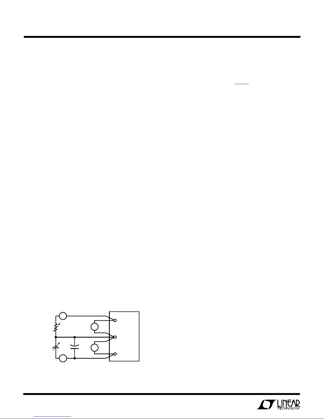
Low-Battery Detector
The LT1317’s low-battery detector is a comparator whose
open collector output appears at the LBO pin of the
LT1317. The inverting input is internally tied to a 200mV
reference and the noninverting input appears at the LBI
pin. The LBI and LBO pins appear at the edge of the DC194.
There are also pads to add a resistor divider (R5 and R6)
from VIN to the LBI pin and a pull-up resistor (R4) from the
LBO to VIN. Figure 7 shows two applications of the lowbattery detector. The first shows its intended use, as an
input voltage monitor; the second shows how to use it as
an undervoltage lockout.
8
Figure 6. Above Is the Transient Response of the All-Ceramic
Design to a 50mA Load Step. The Low Impedance of the
Ceramic Output Capacitor Results in Low Output Ripple.
VIN = 3.3V, V
OUT
= 5V
Page 9

OPERATIO
DEMO MANUAL DC194
MICROPOWER BOOST REGULATOR
U
BATTLOW
1.00M
118k
10M
1M
0.01µF
LBO
LBI
V
IN
GND
(a)
V
IN
1.00M
86.6k
10M
(b)
1M
SHDN
LBO
LBI
V
GND
IN
DC194 F07
Figure 7. Here Are Two Applications of the Low-Battery Detector.
In (a) It Is Used to Sense the Battery Voltage and Trips when V
IN
Falls Below 1.75V. In (b) It Is Used as an Undervoltage Lockout;
It Won’t Allow the LT1317 to Begin Switching until VIN Is Above
2.5V. In Both Cases the 10M Resistor Provides Hysteresis
9
Page 10

DEMO MANUAL DC194
MICROPOWER BOOST REGULATOR
UW
PCB LAYOUT A D FIL
Silkscreen Top
DC194 TSLK
DC194 TSP
Solder Paste Top
Solder Mask Top
10
DC194 TSM
DC194 BSM
Solder Mask Bottom
Page 11

UW
PCB LAYOUT A D FIL
DEMO MANUAL DC194
MICROPOWER BOOST REGULATOR
Top Layer
DC194 TL
Information furnished by Linear Technology Corporation is believed to be accurate and reliable.
However, no responsibility is assumed for its use. Linear Technology Corporation makes no represen-
tation that the interconnection of its circuits as described herein will not infringe on existing patent rights.
DC194 BL
Bottom Layer
11
Page 12

DEMO MANUAL DC194
2.000
2.000
A
B
CCC
D
D
D
D
D
D
B
A
A
A
A
A
DC194 FAB
MICROPOWER BOOST REGULATOR
U
PC FAB DRAWI G
NUMBER
SYMBOL
DIAMETER
A
0.094
B
C
0.035
D
NOTES: UNLESS OTHERWISE SPECIFIED
1.MATERIAL: FR4 OR EQUIVALENT EPOXY, 2 OZ COPPER CLAD
THICKNESS 0.062 ± 0.006 TOTAL OF 2 LAYERS
2.FINISH: ALL PLATED HOLES 0.001 MIN/0.0015 MAX
COPPER PLATE ELECTRODEPOSITED TIN-LEAD
COMPOSTION BEFORE REFLOW, SOLDER
MASK OVER BARE COPPER (SMOBC)
3.SOLDER MASK: BOTH SIDES USING LPI OR EQUIVALENT
4.SILKSCREEN: USING WHITE NONCONDUCTIVE EPOXY INK
5.UNUSED SMD COMPONENTS SHOULD BE FREE OF SOLDER
6.FILL UP ALL VIAS WITH SOLDER
7.ALL DIMENSIONS ARE IN INCHES
OF HOLES
0.07
0.02
PLATED
YES
6
2
3
7
NO
YES
YES
Linear Technology Corporation
12
1630 McCarthy Blvd., Milpitas, CA 95035-7417
(408) 432-1900 ● FAX: (408) 434-0507
●
www.linear-tech.com
dc194 LT/TP 0299 500 • PRINTED IN USA
LINEAR TECHNOLOGY CORPORATION 1999
 Loading...