

LT1308A/LT1308B
High Current, Micropower
Single Cell, 600kHz
DC/DC Converters
FEATURES
n
5V at 1A from a Single Li-Ion Cell
n
5V at 800mA in SEPIC Mode from Four NiCd Cells
n
Fixed Frequency Operation: 600kHz
n
Boost Converter Outputs up to 34V
n
Starts into Heavy Loads
n
Automatic Burst Mode™ Operation at
Light Load (LT1308A)
n
Continuous Switching at Light Loads (LT1308B)
n
Low V
n
Pin-for-Pin Upgrade Compatible with LT1308
n
Lower Quiescent Current in Shutdown: 1µA (Max)
n
Improved Accuracy Low-Battery Detector
Switch: 300mV at 2A
CESAT
Reference: 200mV ±2%
n
Available in 8-Lead SO and 14-Lead TSSOP Packages
APPLICATIONS
n
GSM/CDMA Phones
n
Digital Cameras
n
LCD Bias Supplies
n
Answer-Back Pagers
n
GPS Receivers
n
Battery Backup Supplies
n
Handheld Computers
DESCRIPTION
The LT®1308A/LT1308B are micropower, fi xed frequency
step-up DC/DC converters that operate over a 1V to 10V
input voltage range. They are improved versions of the
LT1308 and are recommended for use in new designs.
The LT1308A features automatic shifting to power saving Burst Mode operation at light loads and consumes
just 140µA at no load. The LT1308B features continuous
switching at light loads and operates at a quiescent current of 2.5mA. Both devices consume less than 1µA in
shutdown.
Low-battery detector accuracy is signifi cantly tighter than
the LT1308. The 200mV reference is specifi ed at ±2%
at room and ±3% over temperature. The shutdown pin
enables the device when it is tied to a 1V or higher source
and does not need to be tied to V
internal V
clamp results in improved transient response
C
and the switch voltage rating has been increased to 36V,
enabling higher output voltage applications.
The LT1308A/LT1308B are available in the 8-lead SO and
the 14-lead TSSOP packages.
L, LT, LTC, LTM, Burst Mode, Linear Technology and the Linear logo are registered trademarks
of Linear Technology Corporation. All other trademarks are the property of their respective
owners.
as on the LT1308. An
IN
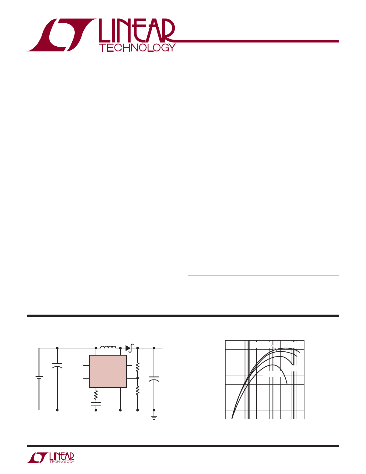
TYPICAL APPLICATION
L1
4.7µH
V
+
C1
47µF
Li-Ion
CELL
C1: AVX TAJC476M010
C2: AVX TPSD227M006
D1: IR 10BQ015
IN
LBI
LT1308B
SHDNSHUTDOWN
V
C
47k
100pF
L1: MURATA LQH6C4R7
*R1: 887k FOR V
Figure 1. LT1308B Single Li-Ion Cell to 5V/1A DC/DC Converter
SW
LBO
GND
OUT
FB
D1
= 12V
R1*
309k
R2
100k
5V
1A
+
C2
220µF
1308A/B F01a
95
90
85
80
75
70
EFFICIENCY (%)
65
60
55
50
1
Converter Effi ciency
VIN = 3.6V
VIN = 1.5V
10 100 1000
LOAD CURRENT (mA)
VIN = 4.2V
VIN = 2.5V
1308A/B F01b
1308abfb
1
LT1308A/LT1308B
ABSOLUTE MAXIMUM RATINGS
VIN, SHDN, LBO Voltage ........................................... 10V
SW Voltage .............................................. –0.4V to 36V
FB Voltage ......................................................... V
Voltage ................................................................. 2V
V
C
+ 1V
IN
LBI Voltage ................................................. –0.1V to 1V
Current into FB Pin ............................................... ±1mA
PIN CONFIGURATION
TOP VIEW
V
1
C
FB
2
SHDN
3
GND
4
8-LEAD PLASTIC SO
T
= 125°C, θJA = 190°C/W
JMAX
S8 PACKAGE
LBO
8
LBI
7
V
6
IN
SW
5
(Note 1)
Operating Temperature Range
Commercial............................................. 0°C to 70°C
Extended Commerial (Note 2) ............ –40°C to 85°C
Industrial ........................................... – 40°C to 85°C
Storage Temperature Range .................. –65°C to 150°C
Lead Temperature (Soldering, 10 sec) ................. 300°C
TOP VIEW
1
V
C
2
FB
3
SHDN
4
GND
5
GND
6
GND
7
GND
F PACKAGE
14-LEAD PLASTIC TSSOP
(NOTE 6)
= 125°C, θJA = 80°C/W
T
JMAX
LBO
14
LBI
13
V
12
IN
V
11
IN
SW
10
SW
9
SW
8
OBSOLETE, FOR INFORMATION PURPOSES ONLY
Contact Linear Technology for Potential Replacement
ORDER INFORMATION
LEAD FREE FINISH TAPE AND REEL PART MARKING PACKAGE DESCRIPTION TEMPERATURE RANGE
LT1308ACS8#PBF LT1308ACS8#TRPBF 1308A 8-Lead Plastic SO 0°C to 70°C
LT1308AIS8#PBF LT1308AIS8#TRPBF 1308AI 8-Lead Plastic SO –40°C to 85°C
LT1308BCS8#PBF LT1308BCS8#TRPBF 1308B 8-Lead Plastic SO 0°C to 70°C
LT1308BIS8#PBF LT1308BIS8#TRPBF 1308BI 8-Lead Plastic SO –40°C to 85°C
LT1308ACF#PBF LT1308ACF#TRPBF LT1308ACF 14-Lead Plastic TSSOP 0°C to 70°C
LT1308BCF#PBF LT1308BCF#TRPBF LT1308BCF 14-Lead Plastic TSSOP 0°C to 70°C
LEAD BASED FINISH TAPE AND REEL PART MARKING PACKAGE DESCRIPTION TEMPERATURE RANGE
LT1308ACS8 LT1308ACS8#TR 1308A 8-Lead Plastic SO 0°C to 70°C
LT1308AIS8 LT1308AIS8#TR 1308AI 8-Lead Plastic SO –40°C to 85°C
LT1308BCS8 LT1308BCS8#TR 1308B 8-Lead Plastic SO 0°C to 70°C
LT1308BIS8 LT1308BIS8#TR 1308BI 8-Lead Plastic SO –40°C to 85°C
LT1308ACF LT1308ACF#TR LT1308ACF 14-Lead Plastic TSSOP 0°C to 70°C
LT1308BCF LT1308BCF#TR LT1308BCF 14-Lead Plastic TSSOP 0°C to 70°C
Consult LTC Marketing for parts specifi ed with wider operating temperature ranges.
For more information on lead free part marking, go to:
This product is only offered in trays. For more information go to:
http://www.linear.com/leadfree/
http://www.linear.com/packaging/
1308abfb
2

LT1308A/LT1308B
ELECTRICAL CHARACTERISTICS
The l denotes the specifi cations which apply over the full operating temperature
range, otherwise specifi cations are at T
= 25°C. Commercial Grade 0°C to 70°C. VIN = 1.1V, V
A
SYMBOL PARAMETER CONDITIONS MIN TYP MAX UNITS
I
Q
Quiescent Current Not Switching, LT1308A
Switching, LT1308B
V
= 0V (LT1308A/LT1308B)
SHDN
V
FB
I
B
Feedback Voltage
FB Pin Bias Current (Note 3)
Reference Line Regulation 1.1V ≤ V
2V ≤ V
IN
≤ 10V
IN
≤ 2V
Minimum Input Voltage 0.92 1 V
g
A
f
m
V
OSC
Error Amp Transconductance ∆I = 5µA 60 µmhos
Error Amp Voltage Gain 100 V/V
Switching Frequency VIN = 1.2V
Maximum Duty Cycle
Switch Current Limit Duty Cycle = 30% (Note 4) 2 3 4.5 A
Switch V
CESAT
Burst Mode Operation Switch Current Limit
ISW = 2A (25°C, 0°C), VIN = 1.5V
I
= 2A (70°C), VIN = 1.5V
SW
= 2.5V, Circuit of Figure 1 400 mA
V
IN
(LT1308A)
Shutdown Pin Current V
SHDN
V
SHDN
V
SHDN
= 1.1V
= 6V
= 0V
LBI Threshold Voltage
LBO Output Low I
LBO Leakage Current V
LBI Input Bias Current (Note 5) V
= 50µA
SINK
= 250mV, V
LBI
= 150mV 33 100 nA
LBI
LBO
= 5V
Low-Battery Detector Gain 3000 V/V
Switch Leakage Current V
SW
= 5V
= VIN, unless otherwise noted.
SHDN
140
2.5
0.01
l
1.20 1.22 1.24 V
l
l
27 80 nA
0.03
0.01
l
500 600 700 kHz
l
82 90 %
290
330
l
l
l
196
l
194
l
l
l
2
20
0.01
200
200
0.1 0.25 V
0.01 0.1 µA
0.01 10 µA
240
4
1
0.4
0.2
350
400
5
35
0.1
204
206
µA
mA
µA
%/V
%/V
mV
mV
µA
µA
µA
mV
mV
The l denotes the specifi cations which apply over the full operating temperature range, otherwise specifi cations are at TA = 25°C.
Industrial Grade –40°C to 85°C. VIN = 1.2V, V
SYMBOL PARAMETER CONDITIONS MIN TYP MAX UNITS
I
Q
V
FB
I
B
g
m
A
V
Quiescent Current Not Switching, LT1308A
Feedback Voltage
FB Pin Bias Current (Note 3)
Reference Line Regulation 1.1V ≤ V
Minimum Input Voltage 0.92 1 V
Error Amp Transconductance ∆I = 5µA 60 µmhos
Error Amp Voltage Gain 100 V/V
= VIN, unless otherwise noted.
SHDN
Switching, LT1308B
V
= 0V (LT1308A/LT1308B)
SHDN
≤ 2V
IN
2V ≤ V
≤ 10V
IN
l
l
l
l
1.19 1.22 1.25 V
l
l
l
140
240
2.5
0.01
27 80 nA
0.05
0.01
0.4
0.2
4
1
mA
µA
%/V
%/V
1308abfb
µA
3
LT1308A/LT1308B
The l denotes the specifi cations which apply over the full operating temperature
ELECTRICAL CHARACTERISTICS
range, otherwise specifi cations are at TA = 25°C. Industrial Grade –40°C to 85°C. VIN = 1.2V, V
SYMBOL PARAMETER CONDITIONS MIN TYP MAX UNITS
f
OSC
Note 1: Stresses beyond those listed under Absolute Maximum Ratings
may cause permanent damage to the device. Exposure to any Absolute
Maximum Rating condition for extended periods may affect device
reliability and lifetime.
Note 2: The LT1308ACS8, LT1308ACF, LT1308BCS8 and LT1308BCF are
designed, characterized and expected to meet the industrial temperature
limits, but are not tested at –40°C and 85°C. I grade devices are
guaranteed over the –40°C to 85°C operating temperature range.
Note 3: Bias current fl ows into FB pin.
Switching Frequency
Maximum Duty Cycle
Switch Current Limit Duty Cycle = 30% (Note 4) 2 3 4.5 A
Switch V
CESAT
Burst Mode Operation Switch Current Limit
ISW = 2A (25°C, –40°C), VIN = 1.5V
I
= 2A (85°C), VIN = 1.5V
SW
= 2.5V, Circuit of Figure 1 400 mA
V
IN
(LT1308A)
Shutdown Pin Current V
SHDN
V
SHDN
V
SHDN
= 1.1V
= 6V
= 0V
LBI Threshold Voltage
LBO Output Low I
LBO Leakage Current V
LBI Input Bias Current (Note 5) V
= 50µA
SINK
= 250mV, V
LBI
= 150mV 33 100 nA
LBI
LBO
= 5V
Low-Battery Detector Gain 3000 V/V
Switch Leakage Current V
SW
= 5V
Note 4: Switch current limit guaranteed by design and/or correlation to
static tests. Duty cycle affects current limit due to ramp generator (see
Block Diagram).
Note 5: Bias current fl ows out of LBI pin.
Note 6: Connect the four GND pins (Pins 4–7) together at the device.
Similarly, connect the three SW pins (Pins 8–10) together and the two V
pins (Pins 11, 12) together at the device.
= VIN, unless otherwise noted.
SHDN
l
500 600 750 kHz
l
82 90 %
290
330
l
l
2
20
0.01
196
l
193
l
l
l
200
200
0.1 0.25 V
0.01 0.1 µA
0.01 10 µA
350
400
5
35
0.1
204
207
mV
mV
µA
µA
µA
mV
mV
IN
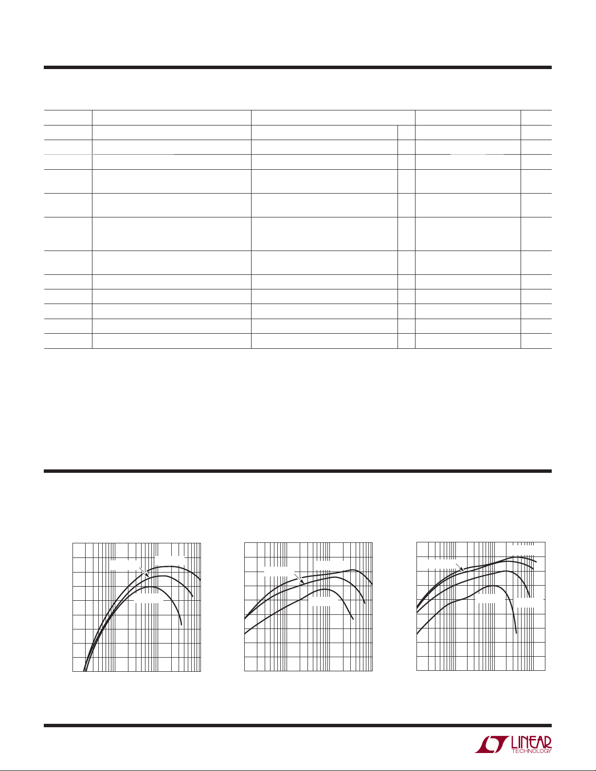
TYPICAL PERFORMANCE CHARACTERISTICS
LT1308B
3.3V Output Effi ciency
95
90
85
80
75
70
EFFICIENCY (%)
65
60
55
50
1 100 1000
VIN = 1.8V
10
LOAD CURRENT (mA)
VIN = 2.5V
VIN = 1.2V
1308A/B G01
LT1308A
3.3V Output Effi ciency
95
90
85
80
75
70
EFFICIENCY (%)
65
60
55
50
VIN = 1.8V
1 100 1000
10
LOAD CURRENT (mA)
VIN = 2.5V
VIN = 1.2V
4
1308A/B G02
LT1308A
5V Output Effi ciency
95
90
VIN = 3.6V
85
80
75
70
EFFICIENCY (%)
65
60
55
50
1
VIN = 4.2V
VIN = 1.5V
10 100 1000
LOAD CURRENT (mA)
VIN = 2.5V
1308A/B G03
1308abfb
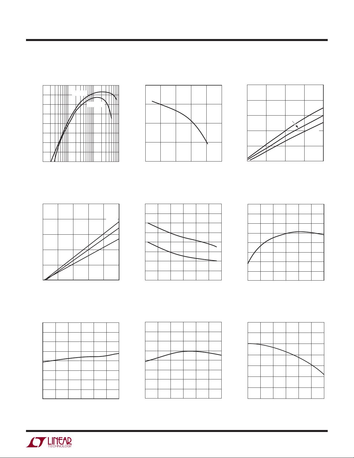
TYPICAL PERFORMANCE CHARACTERISTICS
LT1308A/LT1308B
LT1308B
12V Output Effi ciency
90
85
80
75
70
65
EFFICIENCY (%)
60
55
50
1 100 1000
VIN = 5V
VIN = 3.3V
10
LOAD CURRENT (mA)
SHDN Pin Bias Current vs Voltage
50
40
30
20
SHDN PIN CURRENT (µA)
10
0
2
0
SHDN PIN VOLTAGE (V)
6
4
8
1308A/B G04
–40°C
25°C
85°C
1308 G07
10
Switch Current Limit vs
Duty Cycle
4.0
3.5
3.0
CURRENT LIMIT (A)
2.5
2.0
20
0
40
DUTY CYCLE (%)
FB, LBI Bias Current vs
Temperature
80
70
60
50
40
30
BIAS CURRENT (nA)
20
10
0
–50 –25
LBI
05025
TEMPERATURE (°C)
Switch Saturation Voltage
vs Current
500
400
1.5
85°C
–40°C
2.0
1308 G06
(mV)
300
CESAT
200
SWITCH V
100
0
60
80
100
1308 • G05
0
0.5
SWITCH CURRENT (A)
25°C
1.0
Low Battery Detector Reference
vs Temperature
203
202
201
200
(mV)
199
REF
V
FB
75
100
1308 • G08
198
197
196
195
–50 –25
05025
TEMPERATURE (°C)
75
100
1308 • G09
Oscillator Frequency vs
Temperature
800
750
700
650
600
550
FREQUENCY (kHz)
500
450
400
–50 –2.5
05025
TEMPERATURE (°C)
75
1308 • G10
100
LT1308A Quiescent Current vs
Temperature
180
170
160
150
140
130
120
QUIESCENT CURRENT (µA)
110
100
–50 –25
05025
TEMPERATURE (°C)
75
1308 • G11
100
Feedback Pin Voltage vs
Temperature
1.25
1.24
1.23
1.22
(V)
FB
V
1.21
1.20
1.19
1.18
–50 –25
05025
TEMPERATURE (°C)
75
1308abfb
100
1308 • G12
5

LT1308A/LT1308B
PIN FUNCTIONS
VC (Pin 1/Pin 1): Compensation Pin for Error Amplifi er.
Connect a series RC from this pin to ground. Typical values
are 47k and 100pF. Minimize trace area at V
FB (Pin 2/Pin 2): Feedback Pin. Reference voltage is
1.22V. Connect resistive divider tap here. Minimize trace
area at FB. Set V
V
SHDN (Pin 3/Pin 3): Shutdown. Ground this pin to turn
off switcher. To enable, tie to 1V or more. SHDN does
not need to be at V
GND (Pin 4/Pins 4, 5, 6, 7): Ground. Connect directly
to local ground plane. Ground plane should enclose all
components associated with the LT1308. PCB copper
connected to these pins also functions as a heat sink. For
the TSSOP package, connect all pins to ground copper
to get the best heat transfer. This keeps chip heating to
a minimum.
= 1.22V(1 + R1/R2).
OUT
according to:
OUT
IN
(SO/TSSOP)
to enable the device.
.
C
SW (Pin 5/Pins 8, 9, 10): Switch Pins. Connect inductor/diode here. Minimize trace area at these pins to keep
EMI down. For the TSSOP package, connect all SW pins
together at the package.
(Pin 6/Pins 11, 12): Supply Pins. Must have local
V
IN
bypass capacitor right at the pins, connected directly to
ground. For the TSSOP package, connect both V
together at the package.
LBI (Pin 7/Pin 13): Low-Battery Detector Input. 200mV
reference. Voltage on LBI must stay between –100mV
and 1V. Low-battery detector does not function with
SHDN pin grounded. Float LBI pin if not used.
LBO (Pin 8/Pin 14): Low-Battery Detector Output. Open
collector, can sink 50µA. A 220k pull-up is recommended. LBO is high impedance when SHDN is grounded.
pins
IN
6
1308abfb
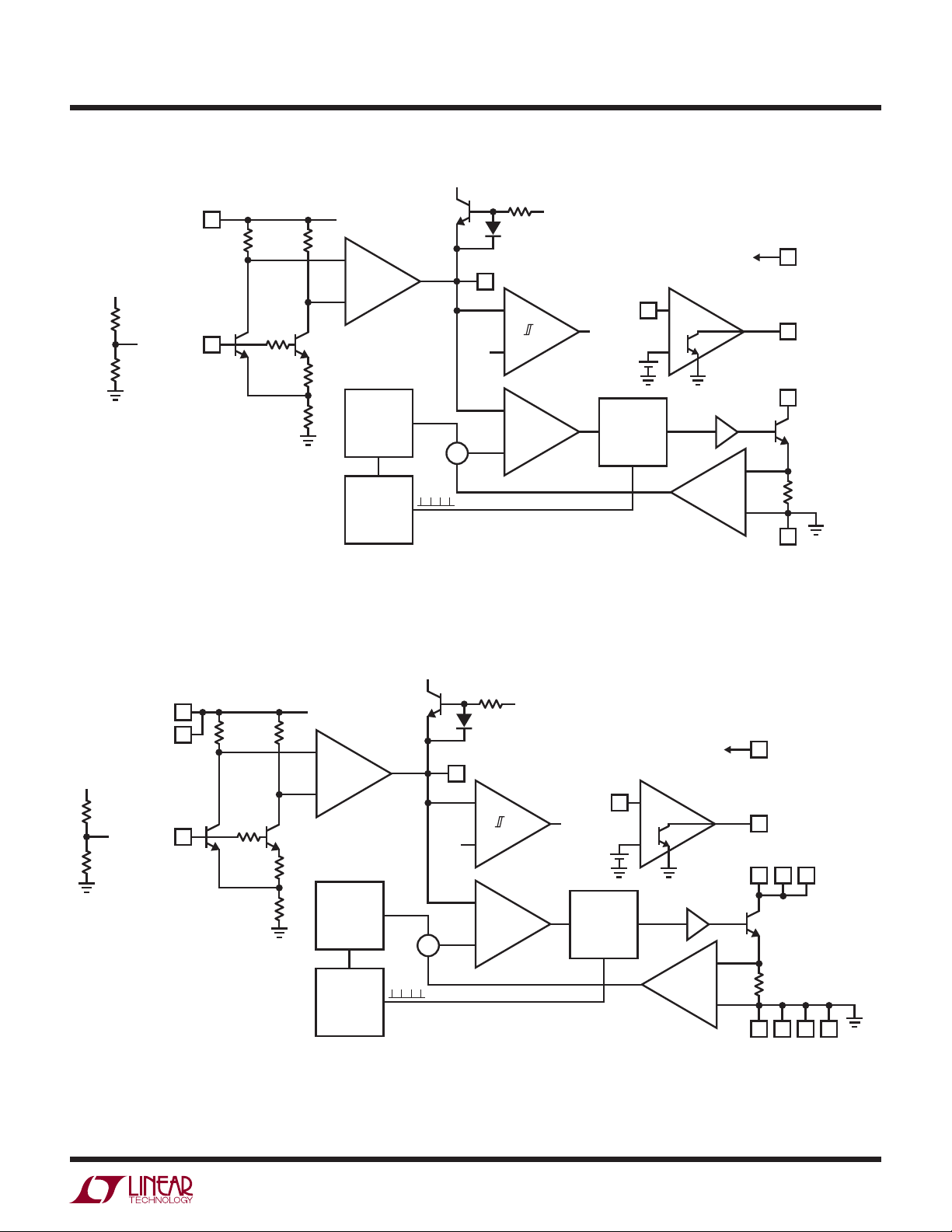
BLOCK DIAGRAMS
V
IN
6
R5
40k
V
OUT
R1
(EXTERNAL)
FB
R2
(EXTERNAL)
FB
Q1
2
R6
40k
Q2
×10
R3
30k
R4
140k
V
IN
+
g
m
–
AMPLIFIER
RAMP
GENERATOR
600kHz
OSCILLATOR
ERROR
V
IN
Q4
V
C
1
2V
BE
+
*
BIAS
–
A1
COMPARATOR
–
+
Σ
+
*HYSTERESIS IN LT1308A ONLY
+
A2
LT1308A/LT1308B
SHUTDOWN
LBI
7
+
ENABLE
–
200mV
R
FF
Q
S
A4
DRIVER
+
A = 3
–
SHDN
3
LBO
8
SW
5
4
GND
Q3
0.03
1308 BD2a
V
OUT
R1
(EXTERNAL)
R2
(EXTERNAL)
Figure 2a. LT1308A/LT1308B Block Diagram (SO-8 Package)
V
IN
+
*
–
A1
COMPARATOR
–
+
A2
2V
BE
SHDN
3
LBO
14
SW
8SW9
SW
10
Q3
ENABLE
200mV
R
SHUTDOWN
LBI
13
+
–
A4
FF
Q
S
DRIVER
+
A = 3
0.03Ω
–
4
GND5GND6GND
GND
7
1308 BD2b
V
11
IN
V
IN
12
R5
40k
R6
40k
V
IN
+
g
m
Q4
V
C
1
–
ERROR
FB
FB
Q1
2
Q2
×10
R3
30k
R4
140k
AMPLIFIER
RAMP
GENERATOR
BIAS
+
Σ
+
600kHz
OSCILLATOR
*HYSTERESIS IN LT1308A ONLY
Figure 2b. LT1308A/LT1308B Block Diagram (TSSOP Package)
1308abfb
7

LT1308A/LT1308B
APPLICATIONS INFORMATION
OPERATION
The LT1308A combines a current mode, fi xed frequency
PWM architecture with Burst Mode micropower operation to maintain high effi ciency at light loads. Operation
can be best understood by referring to the block diagram
in Figure 2. Q1 and Q2 form a bandgap reference core
whose loop is closed around the output of the converter.
When V
is 1V, the feedback voltage of 1.22V, along with
IN
an 80mV drop across R5 and R6, forward biases Q1 and
Q2’s base collector junctions to 300mV. Because this is not
enough to saturate either transistor, FB can be at a higher
voltage than V
above 1.22V, causing V
decrease. When V
. When there is no load, FB rises slightly
IN
(the error amplifi er’s output) to
C
reaches the bias voltage on hyster-
C
etic comparator A1, A1’s output goes low, turning off
all circuitry except the input stage, error amplifi er and
low-battery detector. Total current consumption in this
state is 140µA. As output loading causes the FB voltage to
decrease, A1’s output goes high, enabling the rest of the IC.
Switch current is limited to approximately 400mA initially
after A1’s output goes high. If the load is light, the output
voltage (and FB voltage) will increase until A1’s output goes
low, turning off the rest of the LT1308A. Low frequency
ripple voltage appears at the output. The ripple frequency
is dependent on load current and output capacitance.
This Burst Mode operation keeps the output regulated
and reduces average current into the IC, resulting in high
effi ciency even at load currents of 1mA or less.
If the output load increases suffi ciently, A1’s output
remains high, resulting in continuous operation. When the
LT1308A is running continuously, peak switch current is
controlled by V
to regulate the output voltage. The switch
C
is turned on at the beginning of each switch cycle. When
the summation of a signal representing switch current
and a ramp generator (introduced to avoid subharmonic
oscillations at duty factors greater than 50%) exceeds the
signal, comparator A2 changes state, resetting the fl ip-
V
C
fl op and turning off the switch. Output voltage increases
as switch current is increased. The output, attenuated
by a resistor divider, appears at the FB pin, closing the
overall loop. Frequency compensation is provided by an
external series RC network connected between the V
pin
C
and ground.
Low-battery detector A4’s open-collector output (LBO)
pulls low when the LBI pin voltage drops below 200mV.
There is no hysteresis in A4, allowing it to be used as an
amplifi er in some applications. The entire device is disabled
when the SHDN pin is brought low. To enable the converter,
SHDN must be at 1V or greater. It need not be tied to V
IN
as on the LT1308.
The LT1308B differs from the LT1308A in that there is no
hysteresis in comparator A1. Also, the bias point on A1 is
set lower than on the LT1308B so that switching can occur
at inductor current less than 100mA. Because A1 has no
hysteresis, there is no Burst Mode operation at light loads
and the device continues switching at constant frequency.
This results in the absence of low frequency output voltage
ripple at the expense of effi ciency.
The difference between the two devices is clearly illustrated in Figure 3. The top two traces in Figure 3 shows an
LT1308A/LT1308B circuit, using the components indicated
in Figure 1, set to a 5V output. Input voltage is 3V. Load
current is stepped from 50mA to 800mA for both circuits.
Low frequency Burst Mode operation voltage ripple is
observed on Trace A, while none is observed on Trace B.
At light loads, the LT1308B will begin to skip alternate cycles.
The load point at which this occurs can be decreased by
increasing the inductor value. However, output ripple will
continue to be signifi cantly less than the LT1308A output
ripple. Further, the LT1308B can be forced into micropower
mode, where I
or more out of the V
falls from 3mA to 200µA by sinking 40µA
Q
pin. This stops switching by causing
C
A1’s output to go low.
TRACE A: LT1308A
, 100mV/DIV
V
OUT
AC COUPLED
TRACE B: LT1308B
, 100mV/DIV
V
OUT
AC COUPLED
800mA
I
LOAD
50mA
VIN = 3V
(CIRCUIT OF FIGURE 1)
Figure 3. LT1308A Exhibits Burst Mode Operation Output
Voltage Ripple at 50mA Load, LT1308B Does Not
200µs/DIV
1308 F03
8
1308abfb

APPLICATIONS INFORMATION
LT1308A/LT1308B
Waveforms for a LT1308B 5V to 12V boost converter using
a 10µF ceramic output capacitor are pictured in Figures 4
and 5. In Figure 4, the converter is operating in continuous
mode, delivering a load current of approximately 500mA.
The top trace is the output. The voltage increases as inductor current is dumped into the output capacitor during the
switch off time, and the voltage decreases when the switch
is on. Ripple voltage is in this case due to capacitance,
as the ceramic capacitor has little ESR. The middle trace
is the switch voltage. This voltage alternates between a
V
CESAT
and V
plus the diode drop. The lower trace is
OUT
the switch current. At the beginning of the switch cycle,
the current is 1.2A. At the end of the switch on time, the
current has increased to 2A, at which point the switch turns
off and the inductor current fl ows into the output capacitor
through the diode. Figure 5 depicts converter waveforms
at a light load. Here the converter operates in discontinuous mode. The inductor current reaches zero during the
switch off time, resulting in some ringing at the switch
node. The ring frequency is set by switch capacitance,
diode capacitance and inductance. This ringing has little
energy, and its sinusoidal shape suggests it is free from
harmonics. Minimizing the copper area at the switch node
will prevent this from causing interference problems.
LAYOUT HINTS
The LT1308A/LT1308B switch current at high speed, mandating careful attention to layout for proper performance.
You will not get advertised performance with careless
. Figure 6 shows recommended component place-
layout
ment for an SO-8 package boost (step-up) converter. Follow
this closely in your PC layout. Note the direct path of the
must
switching loops. Input capacitor C1
be placed close
(< 5mm) to the IC package. As little as 10mm of wire or PC
trace from C
to VIN will cause problems such as inability
IN
to regulate or oscillation.
The negative terminal of output capacitor C2 should tie
close to the ground pin(s) of the LT1308A/LT1308B. Doing
this reduces dI/dt in the ground copper which keeps high
frequency spikes to a minimum. The DC/DC converter
ground should tie to the PC board ground plane at one place
only, to avoid introducing dI/dt in the ground plane.
LBI
GROUND PLANE
LBO
C1
+
V
IN
V
OUT
100mV/DIV
V
SW
10V/DIV
I
SW
500mA/DIV
500ns/DIV
1308 F04
Figure 4. 5V to 12V Boost Converter Waveforms in
Continuous Mode. 10μF Ceramic Capacitor Used at Output
V
OUT
20mV/DIV
V
SW
10V/DIV
I
SW
500mA/DIV
500ns/DIV
1308 F05
Figure 5. Converter Waveforms in Discontinuous Mode
R1
SHUTDOWN
MULTIPLE
VIAs
R2
GND
1
2
LT1308A
LT1308B
3
4
8
7
6
5
L1
+
C2
D1
V
OUT
1308 F04
Figure 6. Recommended Component Placement for SO-8
Package Boost Converter. Note Direct High Current Paths
Using Wide PC Traces. Minimize Trace Area at Pin 1 (VC) and
Pin 2 (FB). Use Multiple Vias to Tie Pin 4 Copper to Ground
Plane. Use Vias at One Location Only to Avoid Introducing
Switching Currents into the Ground Plane
Figure 7 shows recommended component placement for
a boost converter using the TSSOP package. Placement
is similar to the SO-8 package layout.
1308abfb
9

LT1308A/LT1308B
APPLICATIONS INFORMATION
GROUND PLANE
R1
R2
SHUTDOWN
MULTIPLE
VIAs
GND
LBI
LBO
C1
+
1
2
3
LT1308A
4
LT1308B
5
6
7
C2
14
13
12
11
10
9
8
+
V
OUT
D1
Figure 7. Recommended Component
Placement for TSSOP Boost Converter.
Placement is Similar to Figure 4
A SEPIC (Single-Ended Primary Inductance Converter)
schematic is shown in Figure 8. This converter topology
produces a regulated output over an input voltage range
V
IN
that spans (i.e., can be higher or lower than) the output.
Recommended component placement for an SO-8 package
SEPIC is shown in Figure 9.
C2
L1
V
IN
3V TO
10V
+
C1
47µF
C1: AVX TAJC476M016
C2: TAIYO YUDEN EMK325BJ475(X5R)
1308 F07
C3: AVX TPSD227M006
L1A
CTX10-2
V
IN
LT1308B
SHDNSHUTDOWN
V
C
47k
680pF
Figure 8. SEPIC (Single-Ended Primary
Inductance Converter) Converts 3V to 10V
Input to a 5V/500mA Regulated Output
4.7µF
CERAMIC
SW
309k
FB
GND
R2
100k
D1: IR 10BQ015
L1: COILTRONICS CTX10-2
D1
L1B
R1
V
OUT
5V
500mA
+
C3
220µF
6.3V
1308A/B F08
GROUND PLANE
R1
R2
SHUTDOWN
MULTIPLE
VIAs
LBI
LBO
C1
+
1
2
LT1308A
LT1308B
3
4
C3
8
7
6
5
V
IN
L1A L1B
C2
+
GND
D1
V
OUT
Figure 9. Recommended Component Placement for SEPIC
1308 F09
1308abfb
10

APPLICATIONS INFORMATION
LT1308A/LT1308B
SHDN PIN
The LT1308A/LT1308B SHDN pin is improved over the
LT1308. The pin does not require tying to V
to enable
IN
the device, but needs only a logic level signal. The voltage
on the SHDN pin can vary from 1V to 10V independent
. Further, fl oating this pin has the same effect as
of V
IN
grounding, which is to shut the device down, reducing
current drain to 1µA or less.
LOW-BATTERY DETECTOR
The low-battery detector on the LT1308A/LT1308B features improved accuracy and drive capability compared
to the LT1308. The 200mV reference has an accuracy of
±2% and the open-collector output can sink 50µA. The
LT1308A/LT1308B low-battery detector is a simple PNP
input gain stage with an open-collector NPN output. The
negative input of the gain stage is tied internally to a 200mV
reference. The positive input is the LBI pin. Arrangement as
a low-battery detector is straightforward. Figure 10 details
hookup. R1 and R2 need only be low enough in value so
that the bias current of the LBI pin doesn’t cause large
errors. For R2, 100k is adequate. The 200mV reference
can also be accessed as shown in Figure 11.
5V
R1
LBI
R2
100k
V
BAT
+
–
200mV
INTERNAL
REFERENCE
GND
V
LT1308A
IN
LT1308B
LBO
1308 F10
100k
R1 =
TO PROCESSOR
V
– 200mV
LB
2µA
A cross plot of the low-battery detector is shown in
Figure 12. The LBI pin is swept with an input which varies from 195mV to 205mV, and LBO (with a 100k pull-up
resistor) is displayed.
V
LBO
1V/DIV
195 205
200
(mV)
V
LBI
1308 F12
Figure 12. Low-Battery Detector
Input/Output Characteristic
START-UP
The LT1308A/LT1308B can start up into heavy loads, unlike
many CMOS DC/DC converters that derive operating voltage
from the output (a technique known as “bootstrapping”).
Figure 13 details start-up waveforms of Figure 1’s circuit
with a 20 load and V
of 1.5V. Inductor current rises to
IN
3.5A as the output capacitor is charged. After the output
reaches 5V, inductor current is about 1A. In Figure 14, the
load is 5 and input voltage is 3V. Output voltage reaches
5V in 500µs after the device is enabled. Figure 15 shows
start-up behavior of Figure 5’s SEPIC circuit, driven from a
9V input with a 10 load. The output reaches 5V in about
1ms after the device is enabled.
V
OUT
2V/DIV
Figure 10. Setting Low-Battery Detector Trip Point
200k
V
BAT
2N3906
V
REF
200mV
10k
+
10µF
LBO
LBI
V
IN
LT1308A
LT1308B
GND
1308 F11
Figure 11. Accessing 200mV Reference
I
L1
1A/DIV
V
SHDN
5V/DIV
1ms/DIV
Figure 13. 5V Boost Converter of Figure 1.
Start-Up from 1.5V Input into 20 Load
1308 F13
1308abfb
11

LT1308A/LT1308B
APPLICATIONS INFORMATION
V
OUT
1V/DIV
I
L1
2A/DIV
V
SHDN
5V/DIV
500µs/DIV
1308 F14
Figure 14. 5V Boost Converter of Figure 1.
Start-Up from 3V Input into 5 Load
V
OUT
2V/DIV
I
SW
2A/DIV
V
SHDN
5V/DIV
500µs/DIV
1308 F15
Figure 15. 5V SEPIC Start-Up from 9V Input into 10 Load
Soft-Start
In some cases it may be undesirable for the LT1308A/
LT1308B to operate at current limit during start-up, e.g.,
when operating from a battery composed of alkaline cells.
The inrush current may cause suffi ciency internal voltage
drop to trigger a low-battery indicator. A programmable
soft-start can be implemented with 4 discrete components. A 5V to 12V boost converter using the LT1308B
is detailed in Figure 16. C4 differentiates V
a current to fl ow into R3 as V
increases. When this
OUT
, causing
OUT
current exceeds 0.7V/33k, or 21µA, current fl ows into
the base of Q1. Q1’s collector then pulls current out the
pin, creating a feedback loop where the slope of V
V
C
is limited as follows:
ΔV
OUT
Δt
With C4 = 33nF, V
0.7V
=
33k •C4
/t is limited to 640mV/ms. Start-up
OUT
waveforms for Figure 16’s circuit are pictured in Figure 17.
Without the soft-start circuit implemented, the inrush current reaches 3A. The circuit reaches fi nal output voltage in
approximately 250µs. Adding the soft-start components
reduces inductor current to less than 1A, as detailed in
Figure 18, while the time required to reach fi nal output
voltage increases to about 15ms. C4 can be adjusted to
achieve any output slew rate desired.
OUT
V
IN
5V
+
C1
47µF
C1: AVX TAJ476M010
C2: TAIYO YUDEN TMK432BJ106MM
D1: IR 10BQ015
L1: MURATA LQH6C4R7
Q1: 2N3904
SHUTDOWN
C4
33nF
R3
33k
L1
4.7µH
V
IN
SHDN
V
C
R4
33k
Q1
SOFT-START
COMPONENTS
LT1308B
R
C
47k
C
C
100pF
SW
GND
D1
100k
10k
FB
330pF
11.3k
1308 F16
C2
10µF
V
OUT
12V
500mA
Figure 16. 5V to 12V Boost Converter with Soft-Start Components Q1, C4, R3 and R4
1308abfb
12

APPLICATIONS INFORMATION
LT1308A/LT1308B
12V
V
OUT
5V/DIV
5V
I
L1
1A/DIV
V
SHDN
10V/DIV
50µs/DIV
Figure 17. Start-Up Waveforms of Figure 16’s Circuit
without Soft-Start Components
12V
V
OUT
5V
I
L1
1A/DIV
V
SHDN
10V/DIV
5ms/DIV
Figure 18. Start-Up Waveforms of Figure 16’s Circuit
with Soft-Start Components Added
1308 F17
1308 F18
COMPONENT SELECTION
Diodes
We have found ON Semiconductor MBRS130 and International Rectifi er 10BQ015 to perform well. For applications where V
exceeds 30V, use 40V diodes such as
OUT
MBRS140 or 10BQ040.
Height limited applications may benefi t from the use of the
MBRM120. This component is only 1mm tall and offers
performance similar to the MBRS130.
Inductors
Suitable inductors for use with the LT1308A/LT1308B must
fulfi ll two requirements. First, the inductor must be able
to handle current of 2A steady-state, as well as support
transient and start-up current over 3A without inductance
decreasing by more than 50% to 60%. Second, the DCR
of the inductor should have low DCR, under 0.05 so
that copper loss is minimized. Acceptable inductance
values range between 2µH and 20µH, with 4.7µH best for
most applications. Lower value inductors are physically
smaller than higher value inductors for the same current
capability.
Table 1 lists some inductors we have found to perform
well in LT1308A/LT1308B application circuits. This is not
an exclusive list.
Table 1
VENDOR PART NO. VALUE PHONE NO.
Murata LQH6C4R7 4.7µH 770-436-1300
Sumida CDRH734R7 4.7µH 847-956-0666
Coiltronics CTX5-1 5µH 561-241-7876
Coilcraft LPO2506IB-472 4.7µH 847-639-6400
Capacitors
Equivalent Series Resistance (ESR) is the main issue
regarding selection of capacitors, especially the output
capacitors.
The output capacitors specifi ed for use with the LT1308A/
LT1308B circuits have low ESR and are specifi cally
designed for power supply applications. Output voltage
ripple of a boost converter is equal to ESR multiplied by
switch current. The performance of the AVX TPSD227M006
220µF tantalum can be evaluated by referring to Figure 3.
When the load is 800mA, the peak switch current is approximately 2A. Output voltage ripple is about 60mV
, so the
P-P
ESR of the output capacitor is 60mV/2A or 0.03. Ripple
can be further reduced by paralleling ceramic units.
Table 2 lists some capacitors we have found to perform
well in the LT1308A/LT1308B application circuits. This is
not an exclusive list.
Table 2
VENDOR SERIES PART NO. VALUE PHONE NO.
AVX TPS TPSD227M006 220µF, 6V 803-448-9411
AVX TPS TPSD107M010 100µF, 10V 803-448-9411
Taiyo Yuden X5R LMK432BJ226 22µF, 10V 408-573-4150
Taiyo Yuden X5R TMK432BJ106 10µF, 25V 408-573-4150
1308abfb
13

LT1308A/LT1308B
APPLICATIONS INFORMATION
Ceramic Capacitors
Multilayer ceramic capacitors have become popular, due
to their small size, low cost, and near-zero ESR. Ceramic
capacitors can be used successfully in LT1308A/LT1308B
designs provided loop stability is considered. A tantalum
capacitor has some ESR and this causes an "ESR zero" in
the regulator loop. This zero is benefi cial to loop stability.
Ceramics do not have appreciable ESR, so the zero is lost
when they are used. However, the LT1308A/LT1308B have
external compensation pin (V
) so component values can
C
be adjusted to achieve stability. A phase lead capacitor can
also be used to tune up load step response to optimum
levels, as detailed in the following paragraphs.
Figure 19 details a 5V to 12V boost converter using either
a tantalum or ceramic capacitor for C2. The input capacitor has little effect on loop stability, as long as minimum
capacitance requirements are met. The phase lead capacitor C
parallels feedback resistor R1. Figure 20 shows
PL
load step response of a 50mA to 500mA load step using a
47µF tantalum capacitor at the output. Without the phase
lead capacitor, there is some ringing, suggesting the
phase margin is low. C
is then added, and response to
PL
the same load step is pictured in Figure 21. Some phase
margin is restored, improving the response. Next, C2 is
replaced by a 10µF, X5R dielectric, ceramic capacitor.
L1
V
SHDN
V
4.7µH
IN
LT1308B
C
47k
100pF
V
IN
5V
+
C1
47µF
SW
GND
D1
R1
R3
100k
10k
FB
R2
11.3k
C
PL
330pF
V
12V
500mA
C2
OUT
Without C
, load step response is pictured in Figure 22.
PL
Although the output settles faster than the tantalum case,
there is appreciable ringing, again suggesting phase margin
is low. Figure 23 depicts load step response using the 10µF
ceramic output capacitor and C
. Response is clean and
PL
no ringing is evident. Ceramic capacitors have the added
benefi t of lowering ripple at the switching frequency due
to their very low ESR. By applying C
series RC at the V
pin, loop response can be tailored to
C
in tandem with the
PL
optimize response using ceramic output capacitors.
V
OUT
500mV/DIV
I
L1
1A/DIV
500mA
LOAD
CURRENT
CURRENT
50mA
200µs/DIV
1308 F20
Figure 20. Load Step Response of LT1308B 5V to 12V
Boost Converter with 47μF Tantalum Output Capacitor
V
OUT
500mV/DIV
I
L1
1A/DIV
500mA
LOAD
50mA
200µs/DIV
1308 F21
Figure 21. Load Step Response with 47μF Tantalum
Output Capacitor and Phase Lead Capacitor C
V
OUT
500mV/DIV
I
L1
1A/DIV
PL
C1: AVX TAJC476M010
C2: AVX TPSD476M016 (47µF) OR
TAIYO YUDEN TMK432BJ106MM (10µF)
D1: IR 10BQ015
L1: MURATA LQH6C4R7
Figure 19. 5V to 12V Boost Converter
14
1308 F19
LOAD
CURRENT
500mA
50mA
200µs/DIV
1308 F22
Figure 22. Load Step Response with 10μF X5R
Ceramic Output Capacitor
1308abfb

APPLICATIONS INFORMATION
V
OUT
500mV/DIV
I
L1
1A/DIV
500mA
LOAD
CURRENT
50mA
200µs/DIV
1308 F23
V
OUT
VIN = 4.2V
V
OUT
VIN = 3.6V
V
OUT
VIN = 3V
I
LOAD
1mA
1A
V
200mV/DIV
TRACES =
OUT
LT1308A/LT1308B
200µs/DIV
1308 F25
Figure 23. Load Step Response with 10μF X5R
Ceramic Output Capacitor and C
PL
GSM AND CDMA PHONES
The LT1308A/LT1308B are suitable for converting a single
Li-Ion cell to 5V for powering RF power stages in GSM or
CDMA phones. Improvements in the LT1308A/LT1308B
error amplifi ers allow external compensation values to be
reduced, resulting in faster transient response compared
to the LT1308. The circuit of Figure 24 (same as Figure 1,
printed again for convenience) provides a 5V, 1A output
from a Li-Ion cell. Figure 25 details transient response at
the LT1308A operating at a V
of 4.2V, 3.6V and 3V. Ripple
IN
voltage in Burst Mode operation can be seen at 10mA
load. Figure 26 shows transient response of the LT1308B
under the same conditions. Note the lack of Burst Mode
ripple at 10mA load.
Li-Ion
CELL
L1
4.7µH
V
+
C1
47µF
IN
LT1308B
SHDNSHUTDOWN
V
C
47k
100pF
SW
GND
D1
R1
309k
FB
R2
100k
5V
1A
+
C2
220µF
Figure 25. LT1308A Li-Ion to 5V Boost Converter
Transient Response to 1A Load Step
V
OUT
VIN = 4.2V
V
OUT
VIN = 3.6V
V
OUT
VIN = 3V
I
LOAD
1A
10mA
V
TRACES =
OUT
200mV/DIV
100µs/DIV
Figure 26. LT1308B Li-Ion to 5V Boost
Converter Transient Response to 1A Load Step
1308 F26
C1: AVX TAJC476M010
C2: AVX TPSD227M006
D1: IR 10BQ015
L1: MURATA LQH6N4R7
Figure 24. Li-Ion to 5V Boost Converter Delivers 1A
1308A/B F24
1308abfb
15

LT1308A/LT1308B
TYPICAL APPLICATIONS
Triple Output TFTLCD Bias Supply
V
IN
5V
V
3
SHDN
C1
4.7µF
C1:TAIYO-YUDEN JMK212BJ475MG
C2, C3:TAIYO-YUDEN LMK325BJ106MN
C4, C5, C6:TAIYO-YUDEN EMK212BJ105MG
D1: MBRM120
D2,D3,D4: BAT54S
L1: TOKO 817FY-4R7M
220k
100pF
1
V
C
D2
1µF
0.22µF
0.22µF
L1
4.7µH
65
IN
LT1308B
SW
GND
D1
2
FB
4
C4
0.22µF
76.8k
10.7k
V
OFF
–9V
10mA
D3
D4
C5
1µF
C6
1µF
C2, C3
10µF
×2
1308 TA02
V
ON
27V
15mA
AV
DD
10V
500mA
500mV/DIV
500mV/DIV
500mV/DIV
I
LOAD
AV
V
V
OFF
800mA
200mA
TFTLCD Bias Supply Transient Response
DD
ON
100µs/DIV
1308abfb
16

TYPICAL APPLICATIONS
3.3V
REGULATED
Q1
150k
3.3k
100k
47k
324k
40nF EL Panel Driver
V
BAT
3V TO 6V
1µF
V
2M
LBI
V
22nF
49.9k
+
IN
C
100pF
C1
47µF
LT1308A
47pF
3
146
SW
FBLBO
SHDN
GND
T1
1:12
D1
D2
D3
4.3M
17k
SHUTDOWN
LT1308A/LT1308B
C2
1µF
10k
200V
EL PANEL
≤40nF
400V
Q2
2.7V TO 6V
100pF
C1: AVX TAJC476M010
C2: VITRAMON VJ225Y105KXCAT
D1: BAT54
D2, D3: BAV21
Q1: MMBT3906
Q2: ZETEX FCX458
T1: MIDCOM 31105
1308 TA03
High Voltage Supply 350V at 1.2mA SEPIC Converts 3V to 10V Input to a 5V/500mA Regulated Output
10nF
250V
V
IN
+
SHUTDOWN
47k
C1
47µF
10nF
V
SHDN
V
C
IN
LT1308A
GND
T1
1:12
3
146
SW
FB
D3
D2
D1
D4
10M
34.8k
10nF
250V
10nF
250V
V
OUT
350V
1.2mA
V
IN
3V TO
10V
+
C1
47µF
C1: AVX TAJC476M016
C2: TAIYO YUDEN EMK325BJ475(X5R)
C3: AVX TPSD227M006
V
SHDNSHUTDOWN
V
IN
C
47k
L1A
CTX10-2
SW
LT1308B
FB
GND
680pF
D1: IR 10BQ015
L1: COILTRONICS CTX10-2
C2
4.7µF
CERAMIC
R2
100k
R1
309k
D1
L1B
+
V
OUT
5V
500mA
C3
220µF
6.3V
1308A/B TA05
D1, D2, D3: BAV21 200mA, 250V
D4: MBR0540
T1: MIDCOM 31105R L
= 1.5µH
P
1308 TA04
1308abfb
17

LT1308A/LT1308B
PACKAGE DESCRIPTION
8-Lead Plastic Small Outline (Narrow .150 Inch)
.050 BSC
S8 Package
(Reference LTC DWG # 05-08-1610)
.045 ±.005
(4.801 – 5.004)
8
.189 – .197
NOTE 3
7
5
6
.245
MIN
.030 ±.005
TYP
RECOMMENDED SOLDER PAD LAYOUT
.010 – .020
(0.254 – 0.508)
.008 – .010
(0.203 – 0.254)
.016 – .050
NOTE:
1. DIMENSIONS IN
2. DRAWING NOT TO SCALE
3. THESE DIMENSIONS DO NOT INCLUDE MOLD FLASH OR PROTRUSIONS.
MOLD FLASH OR PROTRUSIONS SHALL NOT EXCEED .006" (0.15mm)
(0.406 – 1.270)
INCHES
(MILLIMETERS)
× 45°
.160 ±.005
0°– 8° TYP
.228 – .244
(5.791 – 6.197)
F Package
14-Lead Plastic TSSOP (4.4mm)
(Reference LTC DWG # 05-08-1650)
1.05 ±0.10
.053 – .069
(1.346 – 1.752)
.014 – .019
(0.355 – 0.483)
TYP
1
2
4.90 – 5.10*
(.193 – .201)
14 13 12 11 10 9
.150 – .157
(3.810 – 3.988)
NOTE 3
3
4
.004 – .010
(0.101 – 0.254)
.050
(1.270)
BSC
SO8 0303
8
18
6.60 ±0.10
0.45 ± 0.05
RECOMMENDED SOLDER PAD LAYOUT
4.30 – 4.50**
(.169 – .177)
0.09 – 0.20
(.0035 – .0079)
NOTE:
1. CONTROLLING DIMENSION: MILLIMETERS
2. DIMENSIONS ARE IN
3. DRAWING NOT TO SCALE
*
DIMENSIONS DO NOT INCLUDE MOLD FLASH. MOLD FLASH
SHALL NOT EXCEED .152mm (.006") PER SIDE
**
DIMENSIONS DO NOT INCLUDE INTERLEAD FLASH. INTERLEAD
FLASH SHALL NOT EXCEED .254mm (.010") PER SIDE
0.50 – 0.75
(.020 – .030)
4.50 ±0.10
MILLIMETERS
(INCHES)
0.65 BSC
0.25
REF
0° – 8°
0.65
(.0256)
BSC
0.19 – 0.30
(.0075 – .0118)
13456
2
TYP
6.40
(.252)
BSC
7
1.10
(.0433)
MAX
0.05 – 0.15
(.002 – .006)
F14 TSSOP 0204
1308abfb

LT1308A/LT1308B
REVISION HISTORY
REV DATE DESCRIPTION PAGE NUMBER
B 12/10 Obsoleted F Package 2
(Revision history begins at Rev B)
Information furnished by Linear Technology Corporation is believed to be accurate and reliable.
However, no responsibility is assumed for its use. Linear Technology Corporation makes no representation that the interconnection of its circuits as described herein will not infringe on existing patent rights.
1308abfb
19

LT1308A/LT1308B
TYPICAL APPLICATION
Li-Ion to 12V/300mA Step-Up DC/DC Converter
2.7V TO 4.2V
+
C1
47µF
Li-Ion
CELL
C1: AVX TAJC476M010
C2: AVX TPSD107M016
D1: IR 10BQ015
L1
4.7µH
V
IN
LT1308B
SHDNSHUTDOWN
V
C
47k
330pF
L1: MURATA LQH6C4R7
SW
GND
D1
R1
887k
FB
R2
100k
+
12V
300mA
C2
100µF
1308A/B TA01
RELATED PARTS
PART NUMBER DESCRIPTION COMMENTS
LT1302 High Output Current Micropower DC/DC Converter 5V/600mA from 2V, 2A Internal Switch, 200µA I
LT1304 2-Cell Micropower DC/DC Converter 5V/200mA, Low-Battery Detector Active in Shutdown
LT1307/LT1307B Single Cell, Micropower, 600kHz PWM DC/DC Converters 3.3V at 75mA from One Cell, MSOP Package
LT1316 Burst Mode
LT1317/LT1317B Micropower, 600kHz PWM DC/DC Converters 100µA I
®
1474 Micropower Step-Down DC/DC Converter 94% Effi ciency, 10µA IQ, 9V to 5V at 250mA
LT C
LTC1516 2-Cell to 5V Regulated Charge Pump 12µA I
Operation DC/DC with Programmable Current Limit 1.5V Minimum, Precise Control of Peak Current Limit
, Operate with VIN as Low as 1.5V
Q
, No Inudctors, 5V at 50mA from 3V Input
Q
LTC1522 Micropower, 5V Charge Pump DC/DC Converter Regulated 5V ±4% Output, 20mA from 3V Input
LT1610 Single-Cell Micropower DC/DC Converter 3V at 30mA from 1V, 1.7MHz Fixed Frequency
LT1611 Inverting 1.4MHz Switching Regulator in 5-Lead SOT-23 –5V at 150mA from 5V Input, Tiny SOT-23 package
LT1613 1.4MHz Switching Regulator in 5-Lead SOT-23 5V at 200mA from 4.4V Input, Tiny SOT-23 package
LT1615 Micropower Step-Up DC/DC in 5-Lead SOT-23 20µA I
LT1617 Micropower Inverting DC/DC Converter in SOT-23 V
, 36V, 350mA Switch
Q
= 1V to 15V; V
IN
OUT
to –34V
LTC1682 Doubler Charge Pump with Low Noise LDO Adjustable or Fixed 3.3V, 5V Outputs, 60µV
LT1949 600kHz, 1A Switch PWM DC/DC Converter 1.1A, 0.5, 30V Internal Switch, V
as Low as 1.5V
IN
LT1949-1 1.1MHz, 1A Switch DC/DC Converter 1.1MHz Version of LT1949
Q
Output Noise
RMS
20
Linear Technology Corporation
1630 McCarthy Blvd., Milpitas, CA 95035-7417
(408) 432-1900 ● FAX: (408) 434-0507
●
www.linear.com
1308abfb
LT 1210 REV B • PRINTED IN USA
© LINEAR TECHNOLOGY CORPORATION 1999

 Loading...