Linear LT1007CS8, LT1007IS8, LT1037CS8, LT1037IS8 Schematic [ru]

FEATURES
■
Guaranteed
■
Guaranteed
■
0.1Hz to 10Hz Noise, 60nV
■
Guaranteed
■
Guaranteed
■
Guaranteed
■
Guaranteed
■
Guaranteed
■
Guaranteed
4.5nV/√Hz 10Hz Noise
3.8nV/√Hz 1kHz Noise
Typical
P-P
7 Million Min Voltage Gain, RL = 2k
3 Million Min Voltage Gain, RL = 600Ω
25µV Max Offset Voltage
0.6µV/°C Max Drift with Temperature
11V/µs Min Slew Rate (LT1037)
117dB Min CMRR
U
APPLICATIO S
■
Low Noise Signal Processing
■
Microvolt Accuracy Threshold Detection
■
Strain Gauge Amplifiers
■
Direct Coupled Audio Gain Stages
■
Sine Wave Generators
■
Tape Head Preamplifiers
■
Microphone Preamplifiers
LT1007/LT1037
Low Noise, High Speed
Precision Operational Amplifiers
U
DESCRIPTIO
The LT®1007/LT1037 series features the lowest noise
performance available to date for monolithic operational
amplifiers: 2.5nV/√Hz wideband noise (less than the noise of
a 400Ω resistor), 1/f corner frequency of 2Hz and 60nV peakto-peak 0.1Hz to 10Hz noise. Low noise is combined with
outstanding precision and speed specifications: 10µV offset
voltage, 0.2µV/°C drift, 130dB common mode and power
supply rejection, and 60MHz gain bandwidth product on the
decompensated LT1037, which is stable for closed-loop
gains of 5 or greater.
The voltage gain of the LT1007/LT1037 is an extremely high
20 million driving a 2kΩ load and 12 million driving a 600Ω
load to ±10V.
In the design, processing and testing of the device, particular
attention has been paid to the optimization of the entire
distribution of several key parameters. Consequently, the
specifications of even the lowest cost grades (the LT1007C
and the LT1037C) have been spectacularly improved compared to equivalent grades of competing amplifiers.
, LTC and LT are registered trademarks of Linear Technology Corporation.
U
TYPICAL APPLICATIO
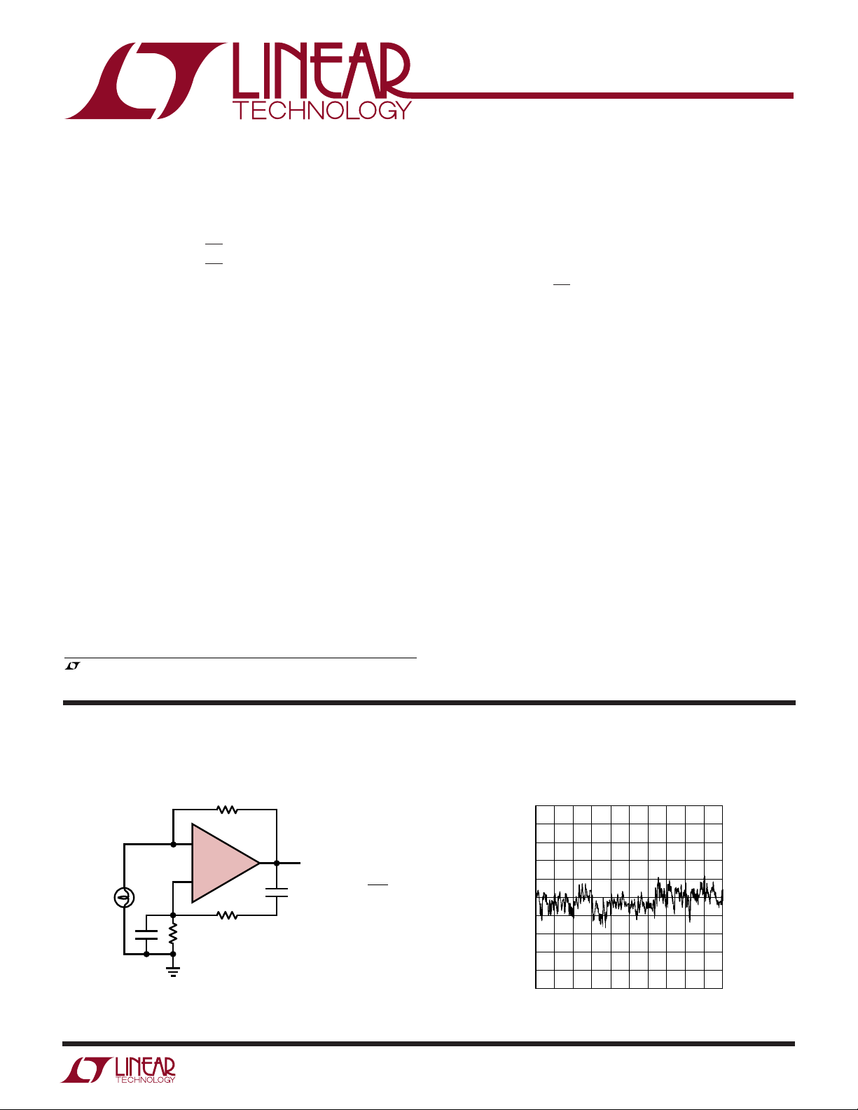
Ultrapure 1kHz Sine Wave Generator
430Ω
–
2
#327 LAMP
LT1037
+
3
CR
TOTAL HARMONIC DISTORTION = < 0.0025%
NOISE = < 0.0001%
AMPLITUDE = ±8V
OUTPUT FREQUENCY = 1.000kHz FOR VALUES GIVEN ±0.4%
6
R
OUTPUT
C
1
f =
2πRC
R = 1591.5Ω ±0.1%
C = 0.1µF ±0.1%
1007/37 TA01
The sine wave generator application shown below utilizes the
low noise and low distortion characteristics of the LT1037.
0.1Hz to 10Hz Noise
VOLTAGE NOISE (20nV/DIV)
0246
TIME (SEC)
8
1007/37 TA02
sn100737 100737fbs
10
1

LT1007/LT1037
TOP VIEW
S8 PACKAGE
8-LEAD PLASTIC SO
1
2
3
4
8
7
6
5
V
OS
TRIM
V
OS
TRIM
V
+
OUT
NC
–IN
+IN
V
–
–
+
WW
W
ABSOLUTE MAXIMUM RATINGS
Supply Voltage ...................................................... ±22V
Input Voltage ............................ Equal to Supply Voltage
U
(Note 1)
Lead Temperature (Soldering, 10 sec.)................. 300°C
Operating Temperature Range
Output Short-Circuit Duration.......................... Indefinite
Differential Input Current (Note 9) ..................... ±25mA
Storage Temperature Range ................. –65°C to 150°C
U
W
U
PACKAGE/ORDER INFORMATION
TOP VIEW
TOP VIEW
V
OS
1
TRIM
–IN
2
–
+
3
–
4
N8 PACKAGE
8-LEAD PDIP
= 100°C, θJA = 130°C/ W (N8)
T
+IN
V
JMAX
V
OS
8
TRIM
+
V
7
OUT
6
NC
5
–IN
T
= 150°C, θJA = 150°C/ W, θJC = 45°C/W
JMAX
ORDER PART NUMBER ORDER PART NUMBER ORDER PART NUMBER
LT1007ACN8
LT1007CN8
LT1007IN8
T
= 150°C, θJA = 100°C/ W (J8)
JMAX
LT1007ACJ8
LT1007AMJ8
LT1007CJ8
LT1007MJ8
LT1037ACN8
LT1037CN8
LT1037IN8
J8 PACKAGE
LEAD CERDIP
LT1037ACJ8
LT1037AMJ8
LT1037CJ8
LT1037MJ8
LT1007ACH
LT1007AMH
LT1007CH
LT1007MH
OBSOLETE PACKAGE OBSOLETE PACKAGE
Consider the N8 Package for Alternate Source Consider the N8 or S8 Package for Alternate Source
Consult LTC Marketing for parts specified with wider operating temperature ranges.
VOS TRIM
1
2
3
8
–
+
4
–
V
(CASE)
H PACKAGE
V
OS
TRIM
+IN
8-LEAD TO-5 METAL CAN
LT1007/LT1037AC, C ............................. 0°C to 70°C
LT1007/LT1037I ............................... –40°C to 85°C
LT1007/LT1037AM, M (OBSOLETE) –55°C to 125°C
+
V
7
6
OUT
5
NC
T
= 150°C, θJA = 190°C/W
JMAX
LT1007CS8
LT1007IS8
LT1037CS8
LT1037IS8
S8 PART MARKING
LT1037ACH
LT1037AMH
LT1037CH
1007
1007I
1037
1037I
LT1037MH
ELECTRICAL CHARACTERISTICS
SYMBOL PARAMETER CONDITIONS MIN TYP MAX MIN TYP MAX UNITS
V
OS
∆V
OS
∆Time
I
OS
I
B
e
n
i
n
Input Offset Voltage (Note 2) 10 25 20 60 µV
Long Term Input Offset (Notes 3, 4) 0.2 1.0 0.2 1.0 µV/Mo
Voltage Stability
Input Offset Current 7 30 12 50 nA
Input Bias Current ±10 ±35 ±15 ±55 nA
Input Noise Voltage 0.1Hz to 10Hz (Notes 4, 6) 0.06 0.13 0.06 0.13 µV
Input Noise Voltage Density fO = 10Hz (Notes 4, 5) 2.8 4.5 2.8 4.5 nV/√Hz
= 1000Hz (Note 4) 2.5 3.8 2.5 3.8 nV/√Hz
f
O
Input Noise Current Density fO = 10Hz (Notes 4, 7) 1.5 4.0 1.5 4.0 pA/√Hz
fO = 1000Hz (Notes 4, 7) 0.4 0.6 0.4 0.6 pA/√Hz
VS = ±15V, TA = 25°C, unless otherwise noted.
LT1007AC/AM LT1007C/I/M
LT1037AC/AM LT1037C/I/M
sn100737 100737fbs
2
P-P

LT1007/LT1037
ELECTRICAL CHARACTERISTICS
SYMBOL PARAMETER CONDITIONS MIN TYP MAX MIN TYP MAX UNITS
Input Resistance, Common Mode 7 5 GΩ
Input Voltage Range ±11.0 ±12.5 ±11.0 ±12.5 V
CMRR Common Mode Rejection Ratio VCM = ±11V 117 130 110 126 dB
PSRR Power Supply Rejection Ratio VS = ±4V to ±18V 110 130 106 126 dB
A
VOL
V
OUT
SR Slew Rate LT1007 RL ≥ 2k 1.7 2.5 1.7 2.5 V/µs
GBW Gain Bandwidth LT1007 fO = 100kHz (Note 8) 5.0 8.0 5.0 8.0 MHz
Z
O
P
D
Large-Signal Voltage Gain RL ≥ 2k, VO = ±12V 7.0 20.0 5.0 20.0 V/µV
≥ 1k, VO = ±10V 5.0 16.0 3.5 16.0 V/µV
R
L
≥ 600Ω, VO = ±10V 3.0 12.0 2.0 12.0 V/µV
R
L
Maximum Output Voltage Swing RL ≥ 2k ±13.0 ±13.8 ±12.5 ±13.5 V
≥ 600Ω±11.0 ±12.5 ±10.5 ±12.5 V
R
L
LT1037 A
Product LT1037 f
Open-Loop Output Resistance VO = 0V, IO = 0 70 70 Ω
Power Dissipation LT1007 80 120 80 140 mW
LT1037 80 130 85 140 mW
≥ 5 1115 1115 V/µs
VCL
= 10kHz (Note 8) (A
O
VS = ±15V, TA = 25°C, unless otherwise noted.
LT1007AC/AM LT1007C/I/M
LT1037AC/AM LT1037C/I/M
≥ 5) 45 60 45 60 MHz
VCL
The ● denotes the specifications which apply over the temperature range 0°C ≤ TA ≤ 70°C, VS = ±15V, unless otherwise noted.
LT1007AC LT1007C
LT1037AC LT1037C
SYMBOL PARAMETER CONDITIONS MIN TYP MAX MIN TYP MAX UNITS
V
OS
∆V
OS
∆Temp
I
OS
I
B
CMRR Common Mode Rejection Ratio VCM = ±10.5V ● 114 126 106 120 dB
PSRR Power Supply Rejection Ratio VS = ±4.5V to ±18V ● 106 126 102 120 dB
A
VOL
V
OUT
P
D
Input Offset Voltage (Note 2) ● 20 50 35 110 µV
Average Input Offset Drift (Note 10) ● 0.2 0.6 0.3 1.0 µV/°C
Input Offset Current ● 10 40 15 70 nA
Input Bias Current ● ±14 ±45 ±20 ±75 nA
Input Voltage Range ● ±10.5 ±11.8 ±10.5 ±11.8 V
Large-Signal Voltage Gain RL ≥ 2k, VO = ±10V ● 4.0 18.0 2.5 18.0 V/µV
≥ 1k, VO = ±10V ● 2.5 14.0 2.0 14.0 V/µV
R
L
Maximum Output Voltage Swing RL ≥ 2k ● ±12.5 ±13.6 ±12.0 ±13.6 V
Power Dissipation ● 90 144 90 160 mW
sn100737 100737fbs
3

LT1007/LT1037
ELECTRICAL CHARACTERISTICS
The ● denotes the specifications which apply over the temperature range –40°C ≤ TA ≤ 85°C, VS = ±15V, unless otherwise noted.
LT1007I/LT1037I
SYMBOL PARAMETER CONDITIONS MIN TYP MAX UNITS
V
OS
∆V
OS
∆Temp
I
OS
I
B
CMRR Common Mode Rejection Ratio VCM = ±10.5V ● 105 120 dB
PSRR Power Supply Rejection Ratio VS = ±4.5V to ±18V ● 101 120 dB
A
VOL
V
OUT
P
D
The ● denotes the specifications which apply over the temperature range –55°C ≤ TA ≤ 125°C, VS = ±15V, unless otherwise noted.
SYMBOL PARAMETER CONDITIONS MIN TYP MAX MIN TYP MAX UNITS
V
OS
∆V
OS
∆Temp
I
OS
I
B
CMRR Common Mode Rejection Ratio VCM = ±10.3V ● 112 126 104 120 dB
PSRR Power Supply Rejection Ratio VS = ±4.5V to ±18V ● 104 126 100 120 dB
A
VOL
V
OUT
P
D
For MIL-STD components, please refer to LTC 883C data sheet for test
listing and parameters.
Note 1: Absolute Maximum Ratings are those values beyond which the life
of a device may be impaired.
Note 2: Input Offset Voltage measurements are performed by automatic
test equipment approximately 0.5 seconds after application of power. AM
and AC grades are guaranteed fully warmed up.
Note 3: Long Term Input Offset Voltage Stability refers to the average
trend line of Offset Voltage vs Time over extended periods after the first 30
days of operation. Excluding the initial hour of operation, changes in V
during the first 30 days are typically 2.5µV. Refer to typical performance
curve.
Note 4: This parameter is tested on a sample basis only.
Input Offset Voltage (Note 2) ● 40 125 µV
Average Input Offset Drift (Note 10) ● 0.3 1.0 µV/°C
Input Offset Current ● 20 80 nA
Input Bias Current ● ±25 ±90 nA
Input Voltage Range ● ±10 ±11.7 V
Large-Signal Voltage Gain RL ≥ 2k, VO = ±10V ● 2.0 15.0 V/µV
R
≥ 1k, VO = ±10V ● 1.5 12.0 V/µV
L
Maximum Output Voltage Swing RL ≥ 2k ● ±12.0 ±13.6 V
Power Dissipation ● 95 165 mW
LT1007AM/LT1037AM LT1007M/LT1037M
Input Offset Voltage (Note 2) ● 25 60 50 160 µV
Average Input Offset Drift (Note 10) ● 0.2 0.6 0.3 1.0 µV/°C
Input Offset Current ● 15 50 20 85 nA
Input Bias Current ● ±20 ±60 ±35 ±95 nA
Input Voltage Range ● ±10.3 ±11.5 ±10.3 ±11.5 V
Large-Signal Voltage Gain RL ≥ 2k, VO = ±10V ● 3.0 14.0 2.0 14.0 V/µV
R
≥ 1k, VO = ±10V ● 2.0 10.0 1.5 10.0 V/µV
L
Maximum Output Voltage Swing RL ≥ 2k ● ±12.5 ±13.5 ±12.0 ±13.5 V
Power Dissipation ● 100 150 100 170 mW
Note 5: 10Hz noise voltage density is sample tested on every lot. Devices
100% tested at 10Hz are available on request.
Note 6: See the test circuit and frequency response curve for 0.1Hz to
10Hz tester in the Applications Information section.
Note 7: See the test circuit for current noise measurement in the
Applications Information section.
Note 8: This parameter is guaranteed by design and is not tested.
Note 9: The inputs are protected by back-to-back diodes. Current limiting
resistors are not used in order to achieve low noise. If differential input
OS
voltage exceeds ±0.7V, the input current should be limited to 25mA.
Note 10: The Average Input Offset Drift performance is within the
specifications unnulled or when nulled with a pot having a range of 8kΩ to
20kΩ.
4
sn100737 100737fbs

W
U
TYPICAL PERFORMANCE CHARACTERISTICS
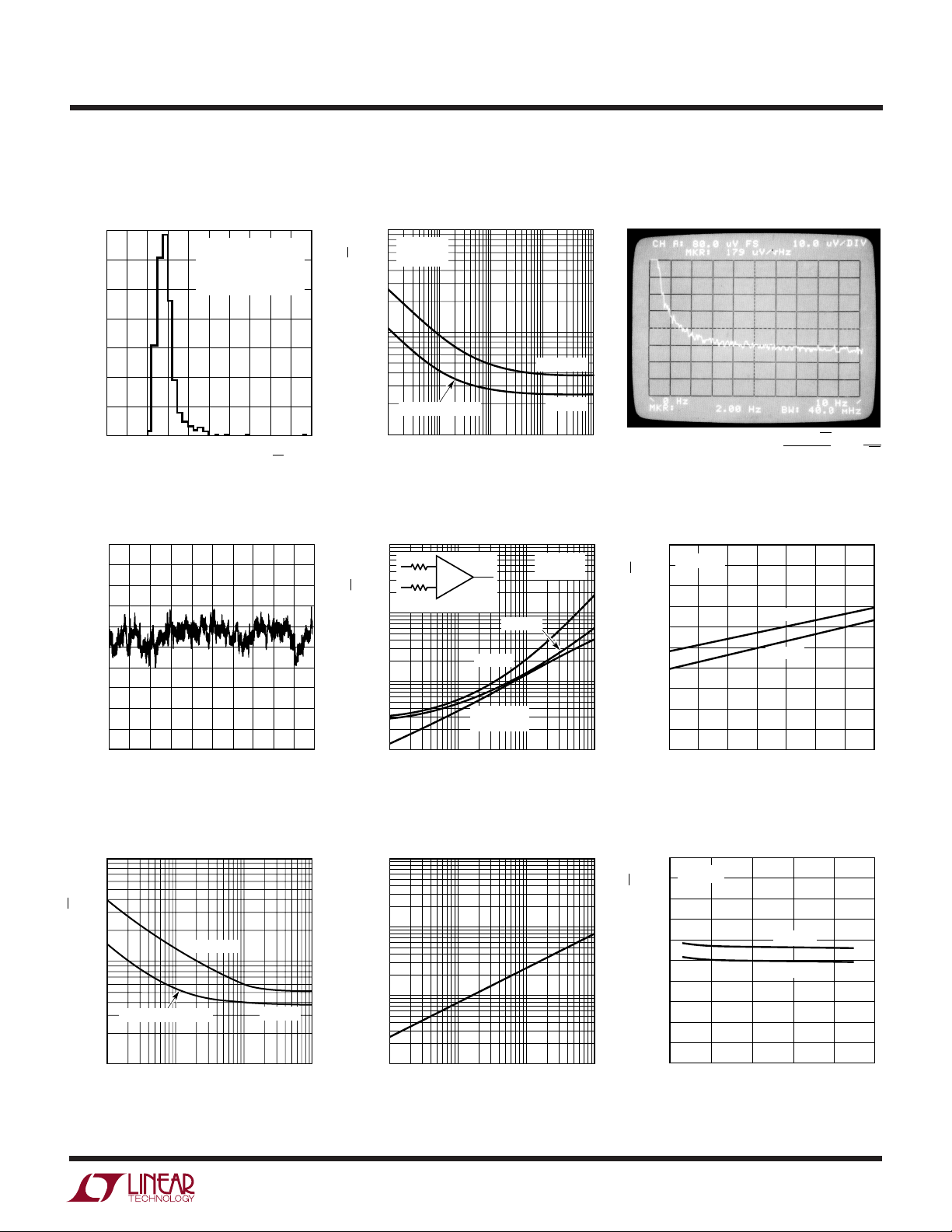
10Hz Voltage Noise Distribution
140
120
100
VS = ±15V
= 25°C
T
A
497 UNITS MEASURED
FROM SIX RUNS
Voltage Noise vs Frequency
100
VS = ±15V
= 25°C
T
A
30
LT1007/LT1037
0.02Hz to 10Hz RMS Noise. Gain = 50,000
(Measured on HP3582 Spectrum Analyzer)
80
60
NUMBER OF UNITS
40
20
0
0
3
1
VOLTAGE NOISE DENSITY (nV/√Hz)
4
2
7
5
68
0.01Hz to 1Hz Peak-to-Peak Noise
VOLTAGE NOISE (20nV/DIV)
0204060
TIME (SEC)
1007/37 G01
80
10
9
100
1007/37 G04
10
3
1/f CORNER = 2Hz
RMS VOLTAGE NOISE DENSITY (nV/√Hz)
1
0.1 100
1
10 1000
FREQUENCY (Hz)
Total Noise vs Source Resistance
1000
100
TOTAL NOISE DENSITY (nV/√Hz)
R
R
SOURCE RESISTANCE = 2R
10
1
0.1
AT 1kHz
AT 10Hz
RESISTOR
NOISE ONLY
1 10 100
SOURCE RESISTANCE (kΩ)
MAXIMUM
TYPICAL
1007/37 G02
VS = ±15V
= 25°C
T
A
1007/37 G05
MARKER AT 2Hz ( = 1/f CORNER) =
Voltage Noise vs Temperature
5
VS = ±15V
4
AT 10Hz
AT 1kHz
25
0
TEMPERATURE (°C)
RMS VOLTAGE NOISE DENSITY (nV/√Hz)
3
2
1
0
–50
–25
179µV/√Hz
50,000
50
75
= 3.59
1007/37 G03
100
1007/37 G06
nV
√Hz
125
Current Noise vs Frequency
10
3
MAXIMUM
100 1k 10k
FREQUENCY (Hz)
RMS NOISE DENSITY (pA/√Hz)
0.3
0.1
1
10
1/f CORNER = 120Hz
TYPICAL
1007/37 G07
Wideband Voltage Noise
(0.1Hz to Frequency Indicated)
10
1
0.1
RMS VOLTAGE NOISE (µV)
0.01
0.1
1 10 100
BANDWIDTH (kHz)
1007/37 G08
Voltage Noise vs Supply Voltage
5
TA = 25°C
4
AT 10Hz
AT 1kHz
15
10
sn100737 100737fbs
RMS VOLTAGE NOISE DENSITY (nV/√Hz)
3
2
1
0
5
0
SUPPLY VOLTAGE (±V)
20
25
1007/37 G09
5

LT1007/LT1037
TIME AFTER POWER ON (MINUTES)
0
CHANGE IN OFFSET VOLTAGE (µV)
10
8
6
4
2
0
4
1007/37 G15
1
2
3
5
VS = ±15V
T
A
= 25°C
DUAL-IN-LINE PACKAGE
PLASTIC (N8) OR CERDIP (J8)
METAL CAN (H) PACKAGE
SUPPLY VOLTAGE (±V)
0
SUPPLY CURRENT (mA)
20
1007/37 G18
5
10
15
4
3
2
1
0
125°C
25°C
–55°C
–1
0
1
–1
0
1
V
S
= ±15V
T
A
= 25°C
INPUT VOLTAGE (µV)
INPUT VOLTAGE (µV)
–15 –10 –5 0 5 10 15
OUTPUT VOLTAGE (V)
MEASURED ON TEKTRONIX 178 LINEAR IC TESTER
1007/37 G12
RL = 2k
R
L
= 600Ω
W
U
TYPICAL PERFORMANCE CHARACTERISTICS
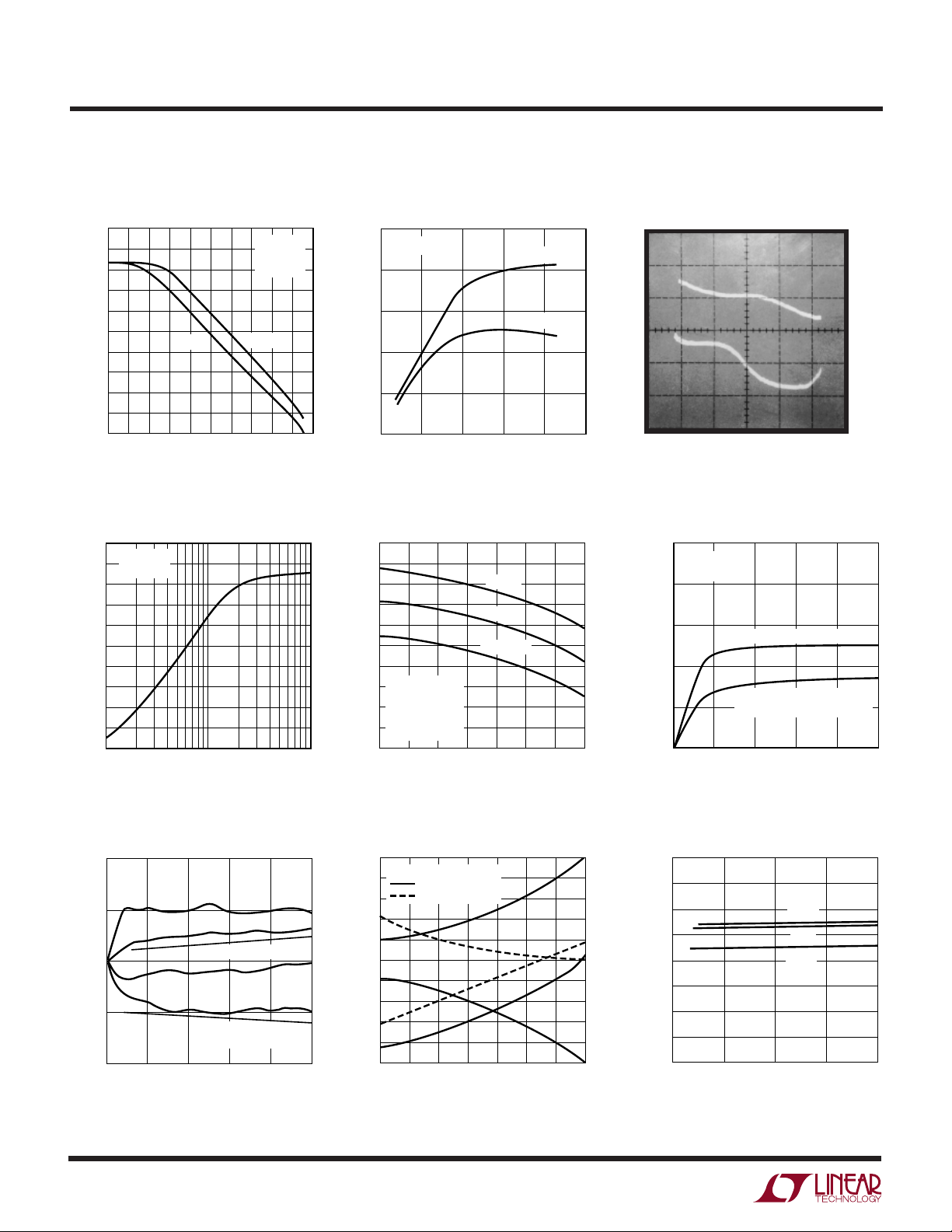
Voltage Gain vs Frequency
180
160
140
120
100
80
60
VOLTAGE GAIN (dB)
40
20
0
–20
0.01
0.1
LT1007
10
1
FREQUENCY (Hz)
100
10k
1k
Voltage Gain vs Load Resistance
25
VS = ±15V
= 25°C
T
A
20
15
10
5
OPEN-LOOP VOLTAGE GAIN (V/µV)
0
0.1 0.3 3
LOAD RESISTANCE (kΩ)
110
VS = ±15V
T
A
R
L
LT1037
100k
= 25°C
= 2k
10M
1M
1007/37 G10
1007/37 G13
100M
Voltage Gain vs Supply Voltage
25
TA = 25°C
20
15
10
5
OPEN-LOOP VOLTAGE GAIN (V/µV)
0
5
0
SUPPLY VOLTAGE (±V)
15
10
Voltage Gain vs Temperature
25
25
RL = 2k
RL = 1k
RL = 600Ω
50
20
15
10
VS = ±15V
VOLTAGE GAIN (V/µV)
5
0
–50
= ±10V
V
OUT
= ±8V FOR
V
OUT
≥ 100°C AND
T
A
= 600Ω
R
L
–25
0
TEMPERATURE (°C)
RL = 2k
RL = 600Ω
20
75
1007/37 G11
100
1007/37 G14
Voltage Gain, RL = 2k and 600Ω
25
Warm-Up Drift
125
Long Term Stability of Four
Representative Units
10
5
0
–5
OFFSET VOLTAGE CHANGE (µV)
–10
2
0
6
4
TIME (MONTHS)
0.2µV/MONTH
0.2µV/MONTH
TREND LINE
6
8
1007/37 G16
Offset Voltage Drift with Temperature
of Representative Units
50
VS = ±15V
40
30
20
10
0
–10
–20
OFFSET VOLTAGE (µV)
–30
–40
10
–50
–50
LT1007/LT1037
LT1007A/LT1037A
0
–25
TEMPERATURE (°C)
50
25
75
100
1007/37 G17
125
Supply Current vs Supply Voltage
sn100737 100737fbs
 Loading...