

Page 1
LSD SCIENCE & TECHNOLOGY CO., LTD.
item : WiFi module
item code: LSD4WF0459-01D0
Version : V1.1
Lierda Science & Technology Group Co., Ltd
LSD4WF0459-01D0
WiFi module data sheet
Address:Lierda Building, 425 Dengyun Road, Hangzhou, China,Lierda Science & Technology Group Co., Ltd
Tel:0571-89908723 Fax:0571-88256108
Page 2

contents
1 Product Introduction............................................................................................- 4 -
1.1 Product Overview.......................................................................................- 4 -
1.2 Functional features..................................................................................... - 4 -
1.3 Application field.........................................................................................- 5 -
1.4 Structure diagram....................................................................................... - 6 -
2 Module parameters..............................................................................................- 6 -
2.1 WiFi Characteristics................................................................................... - 6 -
2.2 Electrical characteristics............................................................................. - 7 -
2.3 Temperature characteristic.......................................................................... - 7 -
3 Hardware structure.............................................................................................. - 8 -
3.1 Product size................................................................................................ - 8 -
3.2 Pin definition..............................................................................................- 9 -
4 Application reference........................................................................................ - 12 -
4.1 Reference design...................................................................................... - 12 -
4.2 Module secondary welding reference temperature curve.......................... - 13 -
5 Packaging information...................................................................................... - 13 -
5.1 Carton packaging......................................................................................- 13 -
5.2 Inner carton packing................................................................................. - 14 -
5.3 Tape and Reel Packaging.......................................................................... - 15 -
5.4 FCC Warning................................................................................................- 16 -
Address:Lierda Building, 425 Dengyun Road, Hangzhou, China,Lierda Science & Technology Group Co., Ltd
Tel:0571-89908723 Fax:0571-88256108
Page 3
Preface
Thank you for choosing the WiFi modules provided by the Lierda Technology Group
co., Ltd. Please read this user’s manual carefully before use, our company does not
We will not be responsible for any of the property loss or personal injury resulted
from the customer’s improper operation. Please follow the technical specification and
reference design when developing the corresponding products according to the
manual. Our company reserves the right to correct or change information and
descriptions of this manual are subject to the technology development without prior
notice and does not assume any responsibility.
Copyright Statement:
The copyright of this manual belongs to the Lierda technology Group co., Ltd,.
Without the written authorization from our company, anyone fully or partially modify
or copy this manual shall bear the corresponding legal responsibilities.
Address:Lierda Building, 425 Dengyun Road, Hangzhou, China,Lierda Science & Technology Group Co., Ltd
Tel:0571-89908723 Fax:0571-88256108
Page 4

1 Product Introduction
1.1 Product Overview
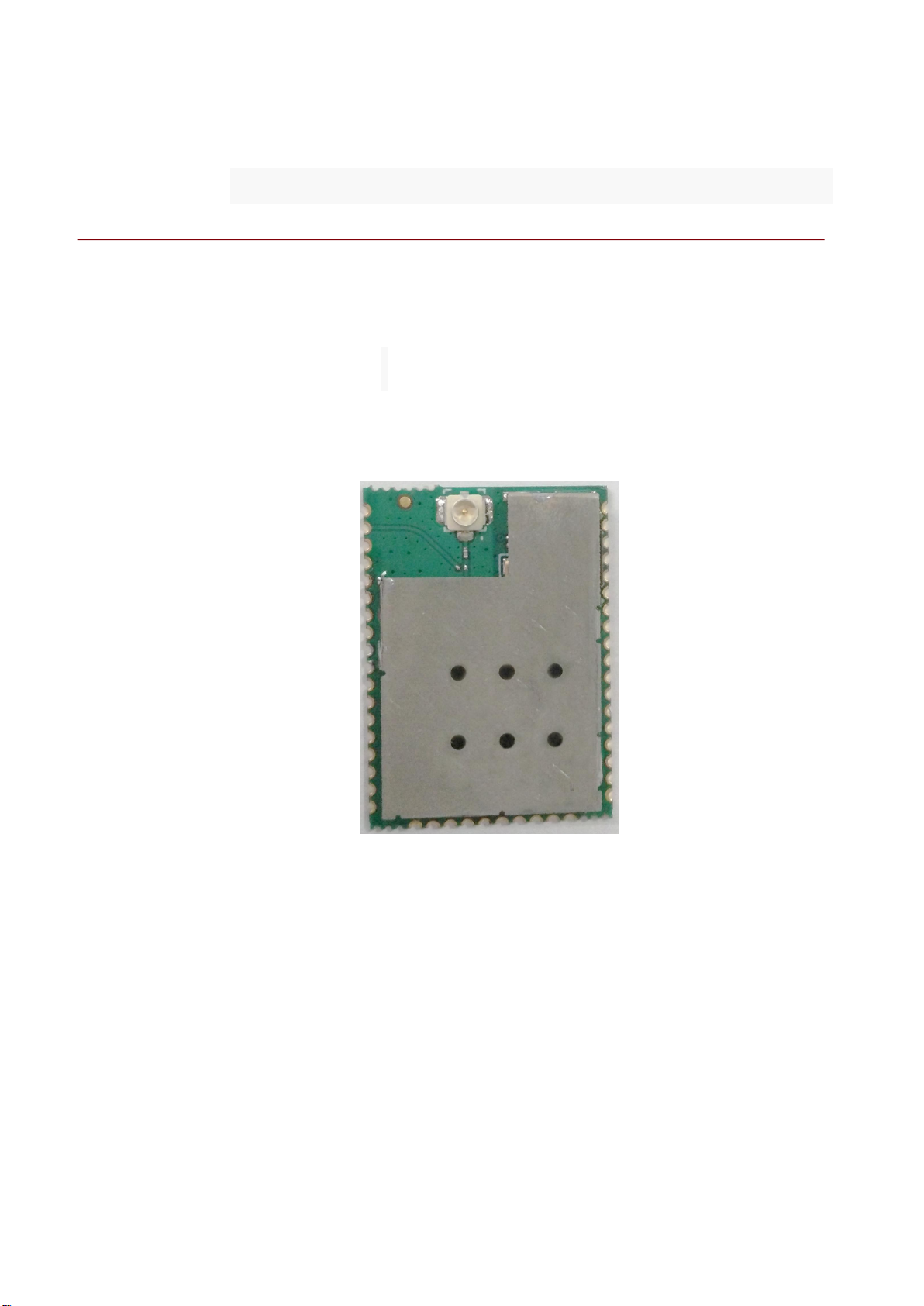
LSD4WF0459-01D0 is a highly integrated WiFi module based on the single chip
controller, Supporting the physical transmission rate of 150 Mbps. Fully comply to
the IEEE 802.11 b/g standard and IEEE 802.11 n standard, In the field of high
standard and the reliability of the transmission, provides a feature-rich wireless
connection scheme.
Optimized radio frequency architecture and Baseband for algorithm provides
excellent rf performance and low power consumption performance. Integration of
MAC design can be configured to efficient DMA engine and data processing cell of
hardware.
In the field of security, service quality and the international standard,
LSD4WF0459-01D0 Provides standard fundamental features, In many applications
environment,it provides good performance to terminal users.
1.2 Functional features
Support IEEE802.11b/g/n client
●
Integrate ARM-CM4 microprocessor
●
●
Embed MAC, several IO interface, highly integrated RF architecture
1T1R model supports 150 Mbps wireless transmission rate in the physical
●
layer
Use the welding plate of stamps hole
●
Address:Lierda Building, 425 Dengyun Road, Hangzhou, China,Lierda Science & Technology Group Co., Ltd
Tel:0571-89908723 Fax:0571-88256108
Page 5

● Small module size and flexible application
● Support WiFi connect directly
● Transmission power control of each packet
● RF signal output is available and external antenna needed
● Embed MCU,support fireware and custom function
1.3 Application field
Smart home, intelligent home appliances products
●
The electronic products which has the function of network: e-books, printers,
●
electronic photo frame;
Industrial remote sensing, telemetry communication.
●
Household wireless security, monitoring, power of computer room, the
●
wireless remote control alarm system of fan device;
Personal navigation equipment, the set-top box GPS
●
POS system,PDA and other wireless intelligent terminal、medical instruments.
●
The electronic stop, intelligent transportation scheduling system
●
;
Address:Lierda Building, 425 Dengyun Road, Hangzhou, China,Lierda Science & Technology Group Co., Ltd
Tel:0571-89908723 Fax:0571-88256108
Page 6
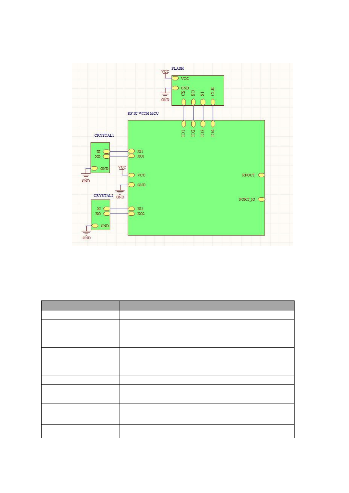
1.4 Structure diagram
Parameter
Specifications
inetrface
IO interface
Wireless LAN standard
Accord with the standard of IEEE 802.11b/g/n
Data rate
11b/g:54,48,36,24,18,12,9,6,11,5.5,2,1 Mbps
11n:20MHz
Modulation mode
802.11g/n---OFDM(BPSK,QPSK,16QAM,64QAM)
802.11b---CCK 11Mbps,5.5Mbp , QPSK 2Mbps ,
BPSK 1Mbps
Frequency range
2.4GHz WiFi frequency band
Operating
frequency
Operation channel
Deviation index
±20ppm
2 Module parameters
2.1 WiFi Characteristics
TA=25℃,VCC=3.3V
11b:1-11
2.4GHz 11g/n:1-11
Figure1 Structure Diagram
2.4GHz 11b/g/n:2412-2462MHz
Address:Lierda Building, 425 Dengyun Road, Hangzhou, China,Lierda Science & Technology Group Co., Ltd
Tel:0571-89908723 Fax:0571-88256108
Page 7
(15±2)dBm (802.11 CCK,11Mbps)
antenna
RF signal output is available,need external antenna.
Receiving sensitivity
-83dBm @ 11M(802.11b CCK,8% PER)
-68dBm @ 54M(802.11g OFDM,10% PER)
-65dBm @ MCS7(802.11n OFDM with 20MHz ,10%
PER)
humidity
20%-90% no condensation
size(standard)
(W)25×(L)18×(H)3.0mm
parameter
min
typical
max
unit
Working voltage
2.7
3.3
3.6
V
Sleep current
1
mA
quiescent current
5
mA
TX current
300
mA
RX current
70
mA
parameter
min
typical
max
unit
Working temperature
-40
25
85
℃
Storage temperature
-40
25
105
℃
(11±2)dBm(802.11 OFDM,54Mbps)
(10±2)dBm(802.11 HT20 MCS7)
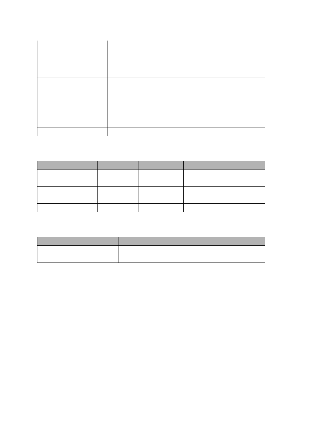
2.2 Electrical characteristics
2.3 Temperature characteristic
Address:Lierda Building, 425 Dengyun Road, Hangzhou, China,Lierda Science & Technology Group Co., Ltd
Tel:0571-89908723 Fax:0571-88256108
Page 8
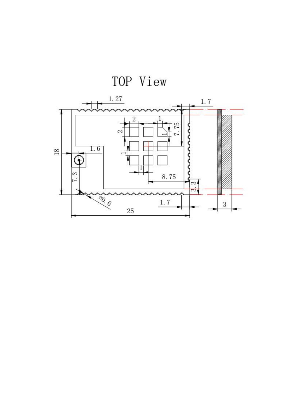
3 Hardware structure
3.1 Product size
unit:mm tolerance standard:GB/T 1804-m
Figure 2 Module Size Figure
Address:Lierda Building, 425 Dengyun Road, Hangzhou, China,Lierda Science & Technology Group Co., Ltd
Tel:0571-89908723 Fax:0571-88256108
Page 9
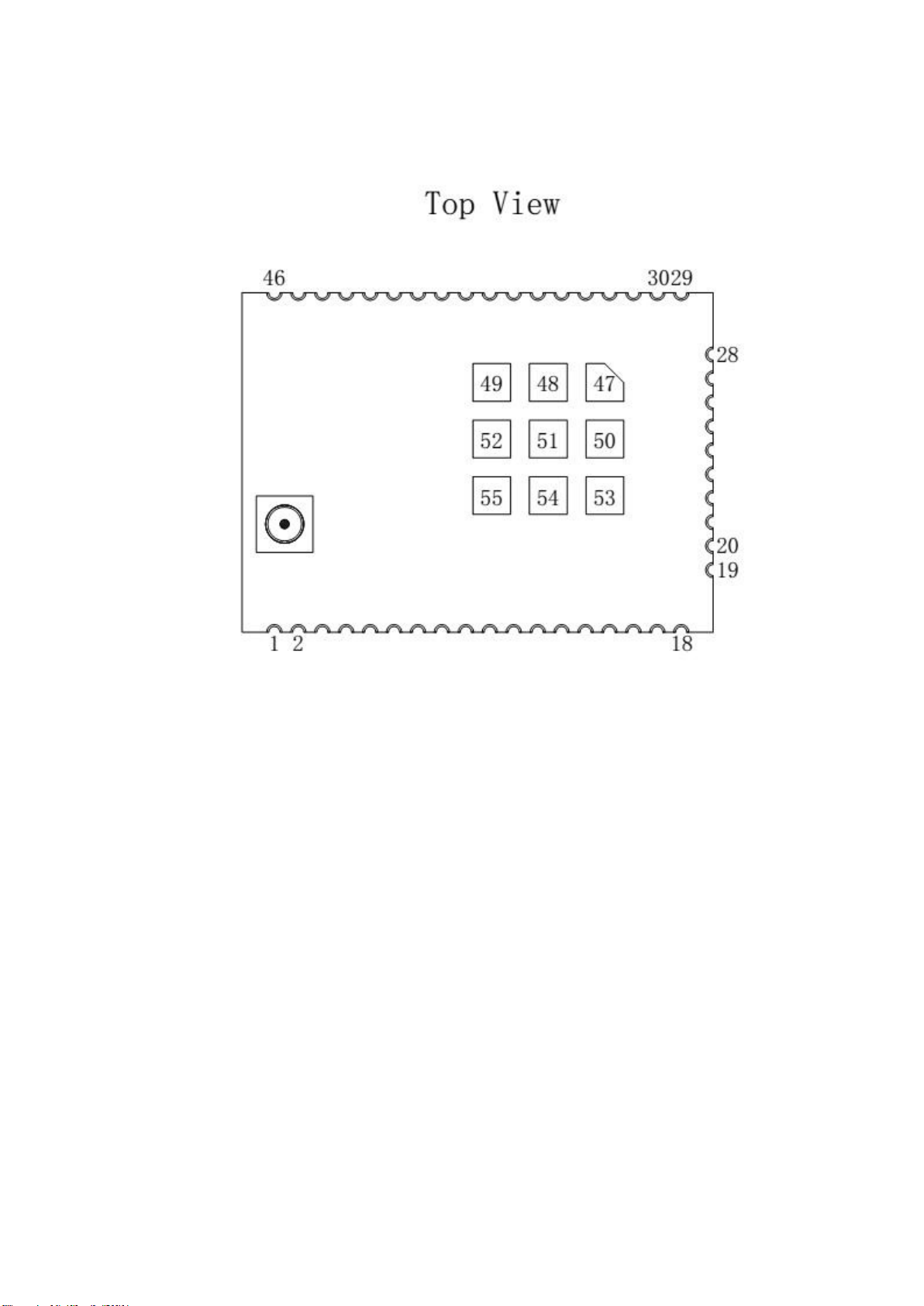
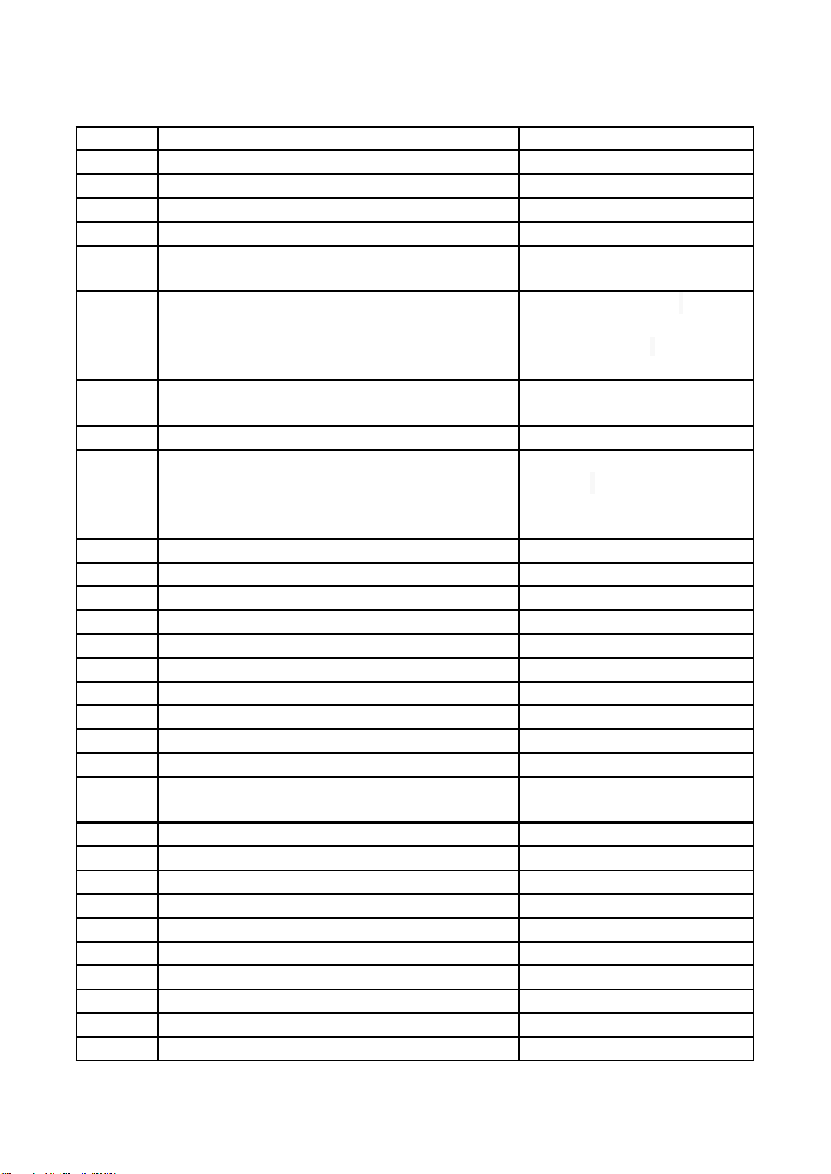
3.2 Pin definition
Figure 3 Figure of Pin Function
Address:Lierda Building, 425 Dengyun Road, Hangzhou, China,Lierda Science & Technology Group Co., Ltd
Tel:0571-89908723 Fax:0571-88256108
Page 10
Address:Lierda Building, 425 Dengyun Road, Hangzhou, China,Lierda Science & Technology Group Co., Ltd
Pin
Pin definition
Functional description
1
GND
GND
2
RF_BG
2.4GHz RF interface
3
GND
GND
4
NC(connect PIN23 by resister and crytals)
NC(dangling)
5
NC(Set aside other models IC 5G in use,
dangling,not connected to any PIN)
NC(dangling)
6
SOP2
Function mode :2.7K Pulldown
resistor ;start UART load
model from falsh.( module has a
drop-down )
7
GPIO28
IO interface(100 k pull-down
resistor in module
)
8
NC(PIN45)
NC
9
SOP0
With SWD mode ,the pin
need 10K Pull-up resistors 。
(100K pull-down resistors in
module)
10
nRESET
Reset pin
11
VBAT_DCDC_ANA
VDD(DC_3.3V
)
12
VBAT_DCDC_PA
VDD(DC_3.3V)
13
VBAT_DCDC_DIG_IO
VDD(DC_3.3V)
14
VDD_FLASH
VDD(DC_3.3V)
15
GPIO30
IO interface
16
NC(PIN48)
NC
17
GPIO0
IO interface
18
NC(connect PIN51 by resister and crytals)
NC(dangling)
19
GND
GND
20
GPIO1
IO interface(100K
pull-down resisteor in module )
21
GPIO2
IO interface
22
GPIO3
IO interface
23
GPIO4
IO interface
24
GPIO5
IO interface
25
GPIO6
IO interface
26
GPIO7
IO interface
27
GPIO8
IO interface
28
GPIO9
IO interface
29
GND
GND
30
GPIO10
IO inetrface
Tel:0571-89908723 Fax:0571-88256108
Page 11
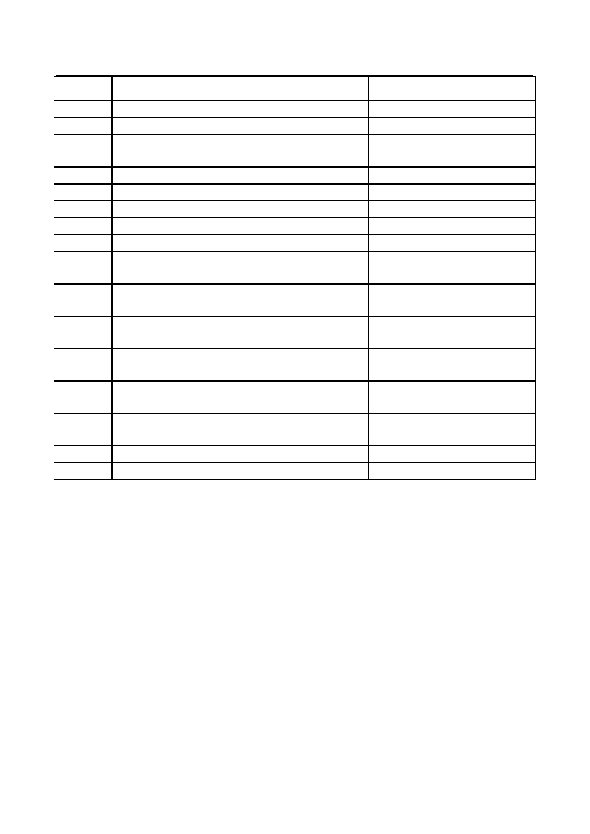
Figure4 Pin Description
31
GPIO11
IO interface
32
GPIO14
IO interface
33
GPIO15
IO interface
34
GPIO16
IO interface(100K pull-down
resistor in module)
35
GPIO17
IO interface
36
GPIO12
IO interface
37
GPIO13
IO interface
38
GPIO22
IO interface
39
JTAG_TDI
JTAG interface/IO interface
40
NC(connect PIN13 by flash DO)
NC(use in external flash
extension)
41
NC(connect PIN14 by flash CS)
NC( use in external flash
extension))
42
NC(connect PIN11 by resistor and flash CLK )
NC( use in external flash
extension))
43
NC( connect PIN12 by flash DI)
NC( use in external flash
extension))
44
JTAG_TDO
JTAG interface/IO
interface)
45
JTAG_TCK
JTAG (100K pull-down
resistor in module)
46
JTAG_TMS
JTAG,dangling if don’t use
47~55
GND
GND
Address:Lierda Building, 425 Dengyun Road, Hangzhou, China,Lierda Science & Technology Group Co., Ltd
Tel:0571-89908723 Fax:0571-88256108
Page 12
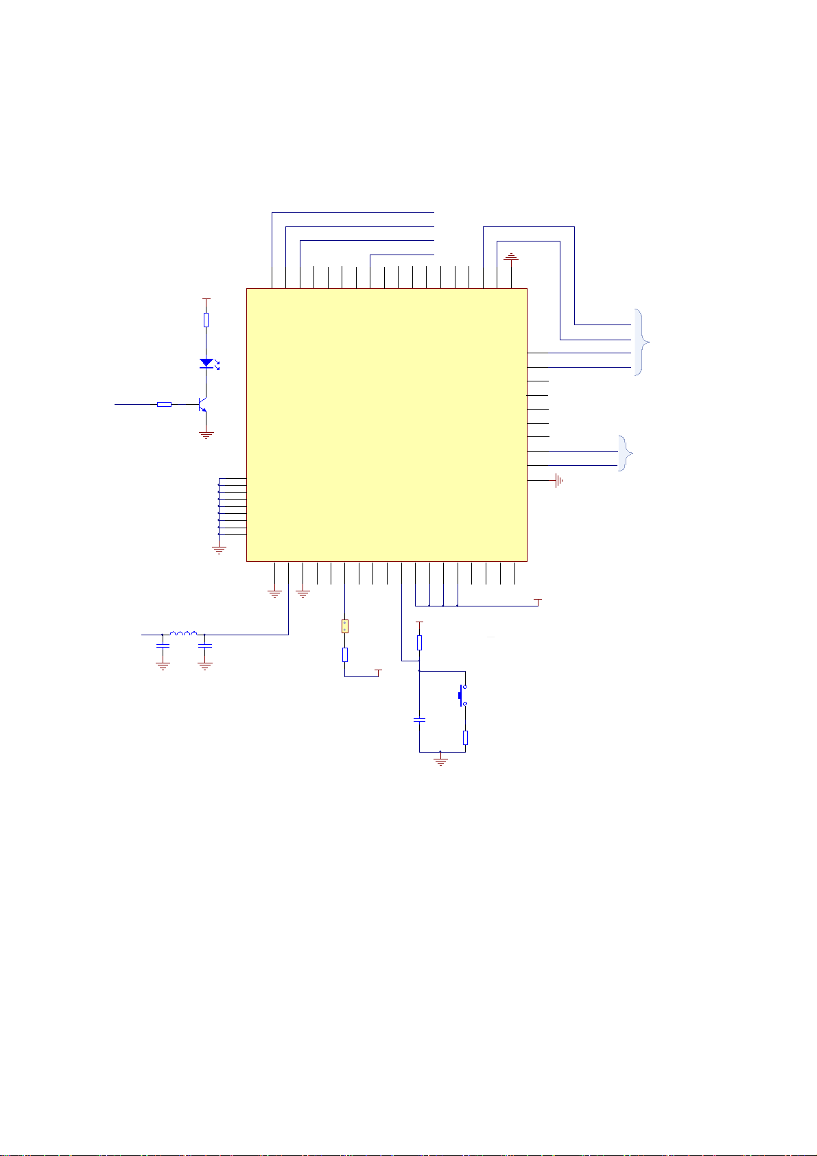
4 Application reference
0
4.1 Reference design
for JTAG
CC_JTAG_TMS
CC_JTAG_TCK
CC_JTAG_TDO
CC_JTAG_TDI
GND
R5
CC_ GPIO_ XX
10K
IO port for LED using
ANT
GND GND
VCC
R4
270R
A K
Q1
8050-S
GND
L1
0R
C2
NC
C1
NC
for ANT matching
46
LED1
47
GND10
48
GND11
49
GND12
50
GND13
51
GND14
52
GND15
53
GND16
54
GND17
55
GND18
50 Ohm RF tr ace
43
44
45
GP IO_29
42
GP IO_24
GP IO_28_TCK
FLASH_SPI_DOUT
39
41
40
FLASH_SPI_CS
FLASH_SPI_DIN
FLASH_SPI_CLK
36
34
35
37
38
GP IO_23
HOST_INTR
HOST_SPI_CS
HO ST_S PI_DO
GP IO_12/I2C_S CL
GP IO_13/I2C_S DA
CC3200 MODULE
RF_B G2GND340M_O SC_BU FF4RF_A5TCXO_EN/GPIO_256GPIO_287VDD_ANA_OUT8SOP09RES ET10VBAT_IN311VBAT_IN212VBAT_IN13GPIO3015VDD_FLASH14VDD_ANA_IN
GND
1
GNDGND
RF
EL 1
MODE update/down load FW normal
SOP2
VCC
J1
R3
1K
VCC
CC_nRES ET
R1
100K
C3
33nF/16V
32
33
HO ST_S PI_DI
HOST_SPI_CLK
WL_DBG_TX/GPIO_05
for RESET
29
30
31
GND
GP IO_10
nHIB/G PIO _11
GPIO_09
GPIO_08
UART 0_ T X/ GPI O_0 7
UART 1_C TS/ GPI O_0 6
RS232_RX/GPIO_04
RS232_TX/GPIO_03
UART1_RX/GPIO_02
UART 1_ T X/ GPI O_0 1
EXT_32K18UA RT1_RTS/G PIO _00
17
16
S1
SW- Q
R2
100R
GND
Reloa rd/CC_GPIO_11
28
27
26
25
24
23
22
21
20
19
Po we r :DC_3 . 3V
VCC
Ready /CC_GPIO_09
Sleep/CC_GPIO_08
GND
Please a dd decoupli ng capaci tor
for state control
Link/ CC_GPIO_10
for UART
UART_ RX
UART _T X
connect to IO ports of MCU
connect to UART ports of MCU
GND
Figure 5 Reference design
Address:Lierda Building, 425 Dengyun Road, Hangzhou, China,Lierda Science & Technology Group Co., Ltd
Tel:0571-89908723 Fax:0571-88256108
Page 13
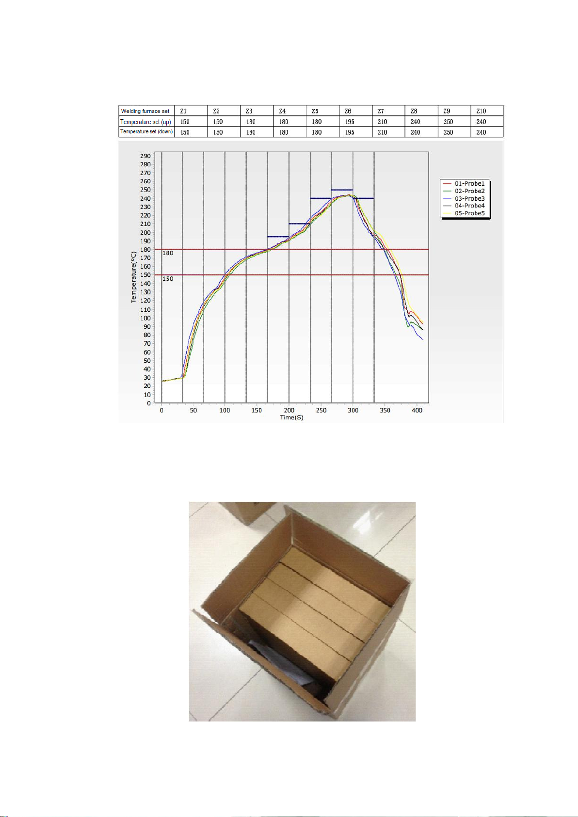
4.2 Module secondary welding reference temperature curve
5 Packaging information
5.1 Carton packaging
Module USES 354 * 250 * 362 mm carton packaging, contain inside the box.
Address:Lierda Building, 425 Dengyun Road, Hangzhou, China,Lierda Science & Technology Group Co., Ltd
Tel:0571-89908723 Fax:0571-88256108
Page 14
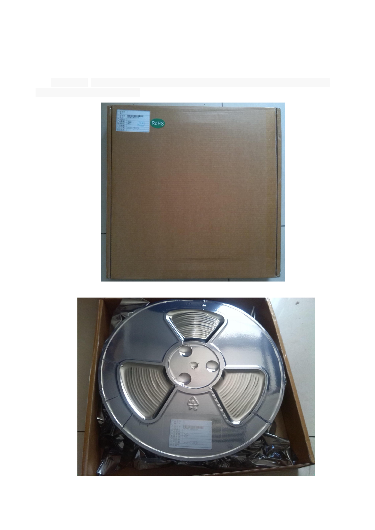
Figure 7 Carton assembly figure
5.2 Inner carton packing
Internal size is 352*348*56mm,each contain a set of vacuum reel packaged by electrostatic
bag, It contains 600 PCS modules.
Figure 8 appearance figure Inside the box
Address:Lierda Building, 425 Dengyun Road, Hangzhou, China,Lierda Science & Technology Group Co., Ltd
Tel:0571-89908723 Fax:0571-88256108
Page 15
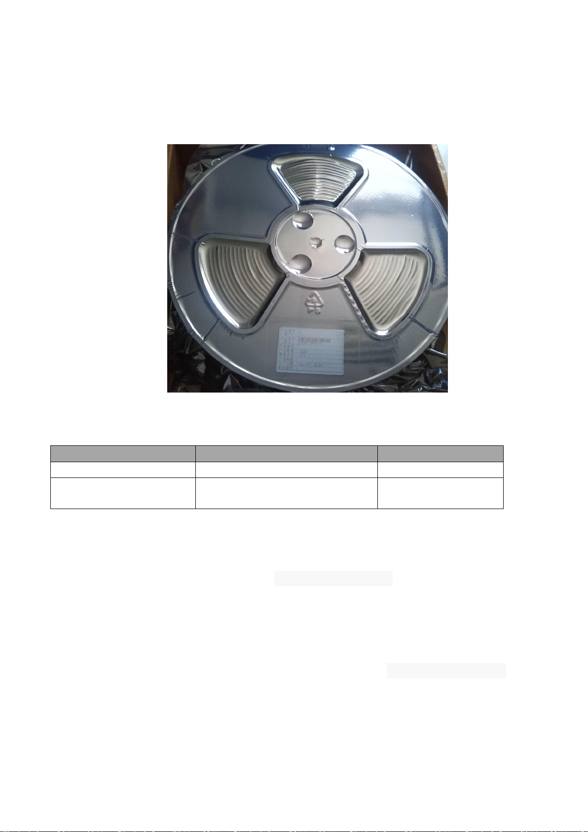
Figure 9 vacuum reel
Version number
Revised scope
Date
V1.0
Create a document
2016-01-18
V1.1
Increase the test environment and
deviation requirements
2016-4-3
5.3 Tape and Reel Packaging
A single module adopts the take-up package,each contains 500PCS module.
Figure 10 rewinding roller
Contact information of the LSD WiFi
----------------------------------------------------------------------------------------------------------------------------------------
WiFi business division of theLierda Science & Technology Group Co., Ltd
www.lierda.com
Address
Group Co., Ltd
Email:[email protected]
----------------------------------------------------------------------------------------------------------------------------------------
:Lierda Building, 425 Dengyun Road, Hangzhou, China,Lierda Science & Technology
Compiler:Lierda Science & Technology Group Co., Ltd
WiFi business division
2016.4
Address:Lierda Building, 425 Dengyun Road, Hangzhou, China,Lierda Science & Technology Group Co., Ltd
Tel:0571-89908723 Fax:0571-88256108
Page 16

5.4 FCC Warning
Any Changes or modifications not expressly approved by the party responsible for compliance could
void the user’s authority to operate the equipment.
This device complies with part 15 of the FCC Rules. Operation is subject to the following two conditions:
(1) This device may not cause harmful interference, and (2) this device must accept any interference
received, including interference that may cause undesired operation.
To satisfy FCC RF Exposure requirements for this transmission devices, a separation distance of 20cm or
more should be maintained between the antenna of this device and persons during operation. To ensure
compliance, operation at closer than this distance is not recommended. The antenna(s) used for this
transmitter must not be co-located or operating in conjunction with any other antenna or transmitter. The
modular transmitter must be equipped with either a permanently affixed label or must be capable of
electronically displaying its FCC identification number:
(A) If using a permanently affixed label, the modular transmitter must be labeled with its own FCC
identification number, and, if the FCC identification number is not visible when the module is installed
inside another device, then the outside of the device into which the module is installed must also display
a label referring to the enclosed module. This exterior label can use wording such as the following:
“Contains Transmitter Module FCC ID:N8NLSD4WF0459.” Any similar wording that expresses the same
meaning may be used. The Grantee may either provide such a label, an example of which must be
included in the application for equipment authorization, or, must provide adequate instructions along with
the module which explain this requirement. In the latter case, a copy of these instructions must be
included in the application for equipment authorization.
Address:Lierda Building, 425 Dengyun Road, Hangzhou, China,Lierda Science & Technology Group Co., Ltd
Tel:0571-89908723 Fax:0571-88256108
 Loading...