

Page 1
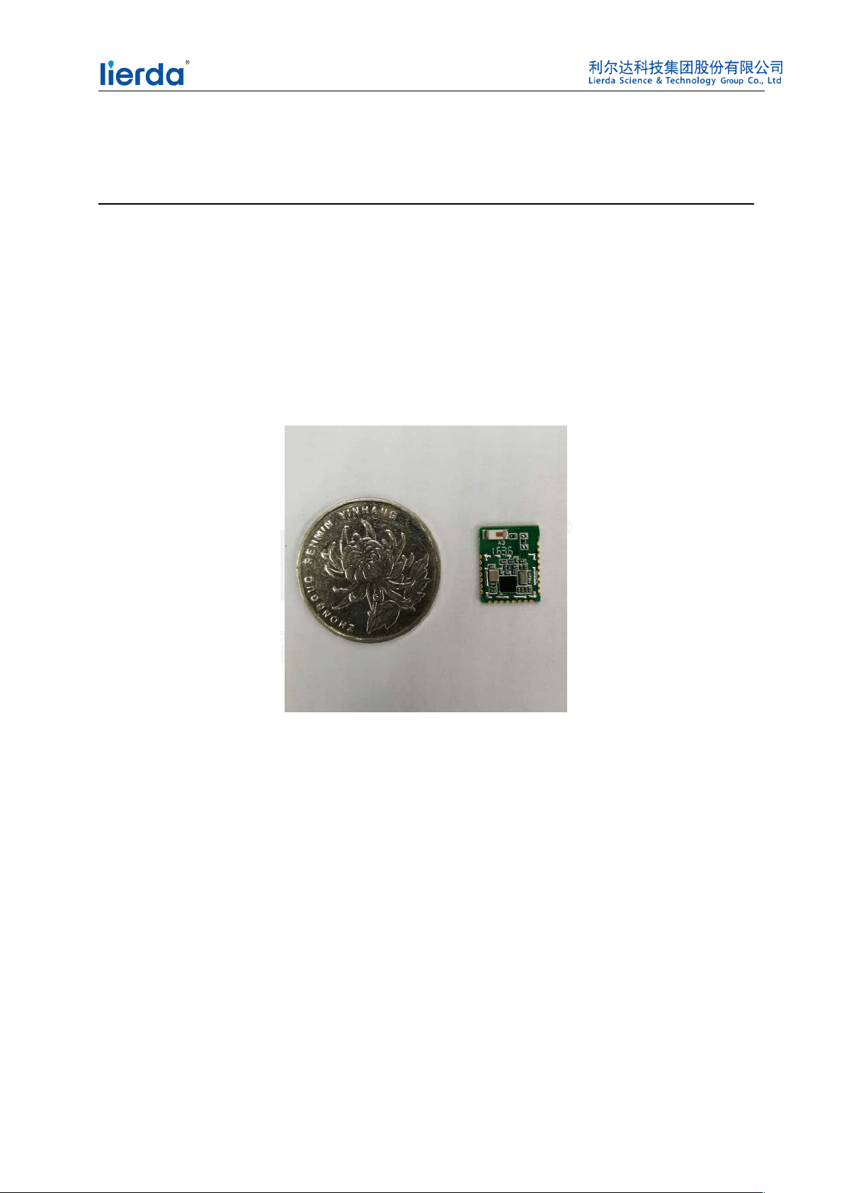
利尔达科技集团股份有限公司
LIERDA SCIENCE & TECHNOLOGY GROP CO.,LTD
LSD1BT-STBLEPCB
Product manual
Product Name:
P/N: LSD1BT-STBLEPCB
Document version: V4.0
BlueNRG-A Bluetooth module PCBA
1
Page 2
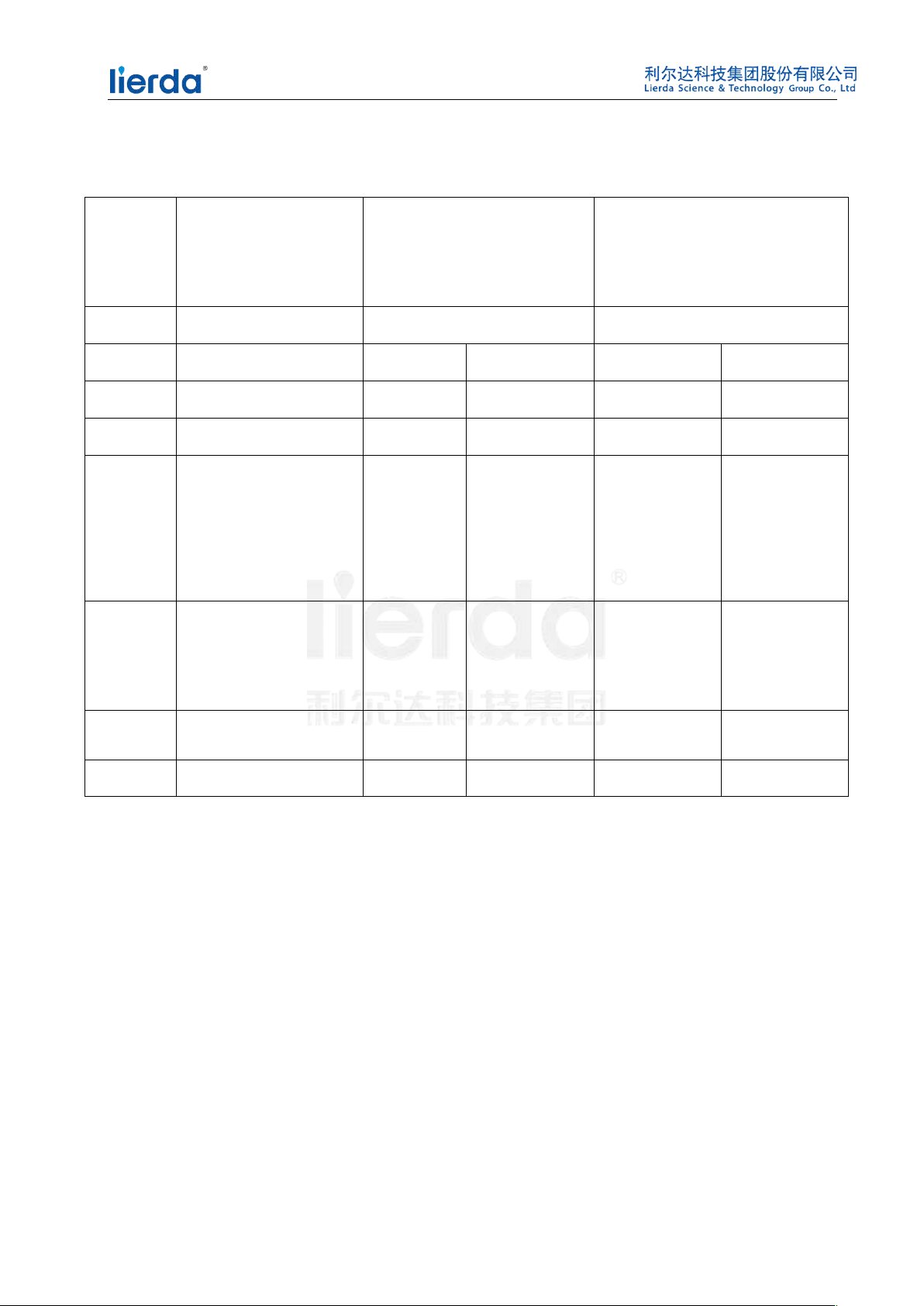
Revision history
Product
Name
BlueNRG-A
Bluetooth module
Product Type LSD1BT-STBLEPCB
PCBA
Editor Qiumg Date 20170726
No. Revision record Modifier Auditor Versions Date
1 Initial release Liuzh V1.0 20161012
2 Liuzh V1.1 20161210
3 Add descriptions of
Marco Qiu V2.0 20170726
product information;
Modify partial data;
Add figure comments
4 The module power is
Marco Qiu V3.0 20171225
divided into BAT1 and
5
6
BAT2 in pin definition
Add FCC&CE
Marco Qiu V4.0 20180108
Information
Marco Qiu V5.0 20180118
2
Page 3
Information
Part Number Description Package Size
LSD1BT-STBLEPCB
The PN is pure hardware without shield or any
firmware. Please contact us if there is other
requirements for second development of end users.
13mm*10mm*2.3mm
-- --
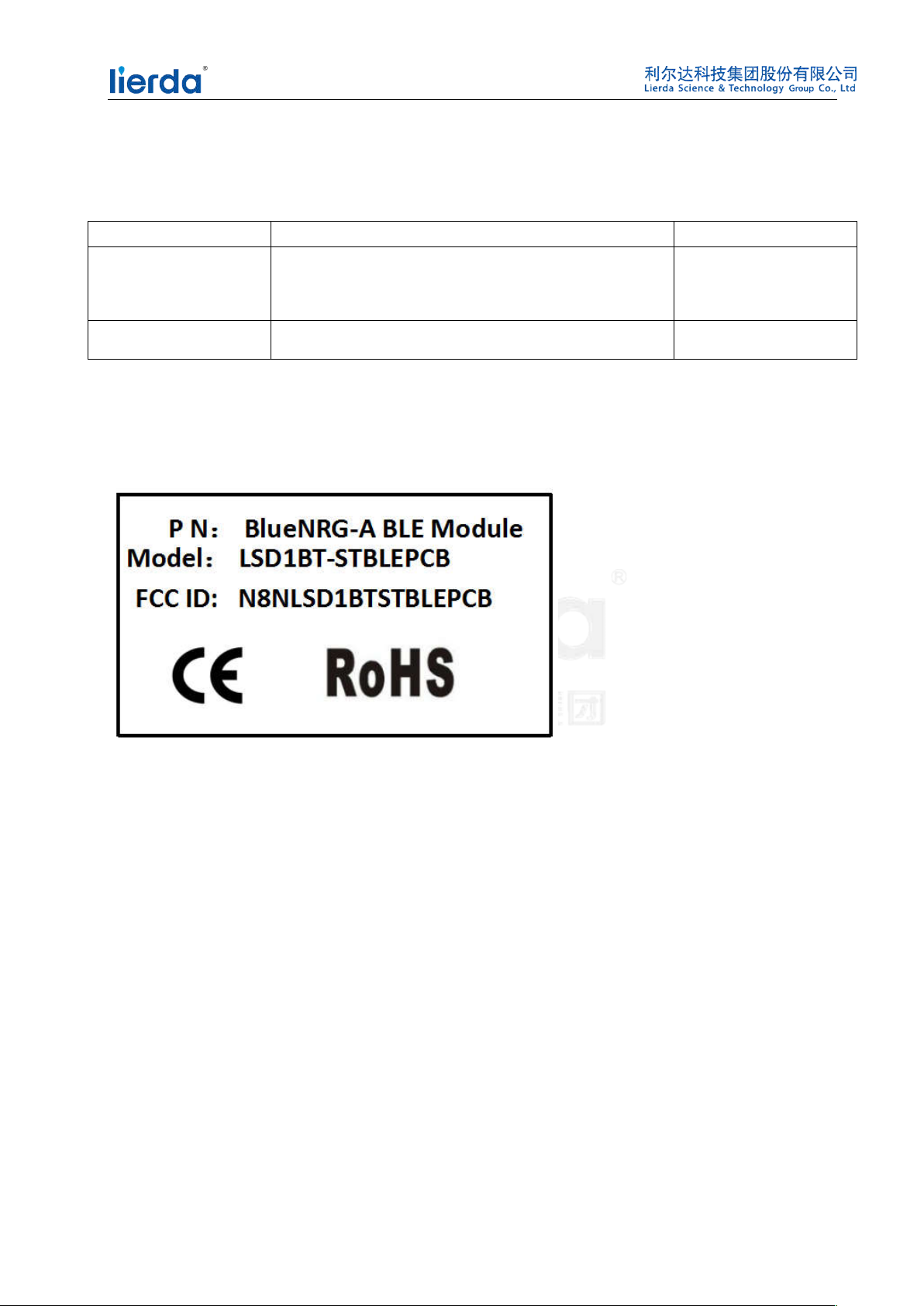
The Label
This device complies with Part 15 of the FCC Rules. Operation is subject to the
--
following two conditions: (1) this device may not cause harmful interference, and (2)
this device must accept any interference received, including interference that may
cause undesired operation.
3
Page 4

Contents
1 Features .......................................................................................................................................................... 5
2 Specifications ................................................................................................................................................. 6
3 Hardware ........................................................................................................................................................ 7
3.1 Dimensions Diagram ........................................................................................................................... 7
3.2 Pin Description .................................................................................................................................... 8
4 Applications .................................................................................................................................................... 9
4.1 Application circuit ............................................................................................................................... 9
4.2 Precautions ........................................................................................................................................ 10
4.3 Download and Debug ........................................................................................................................ 10
4.4 Development board ........................................................................................................................... 10
4.5 Reference manual .............................................................................................................................. 10
5 Federal Communications Commission (FCC) Interference Statement ......................................................... 11
Note ................................................................................................................................................................. 12
4
Page 5
1 Features
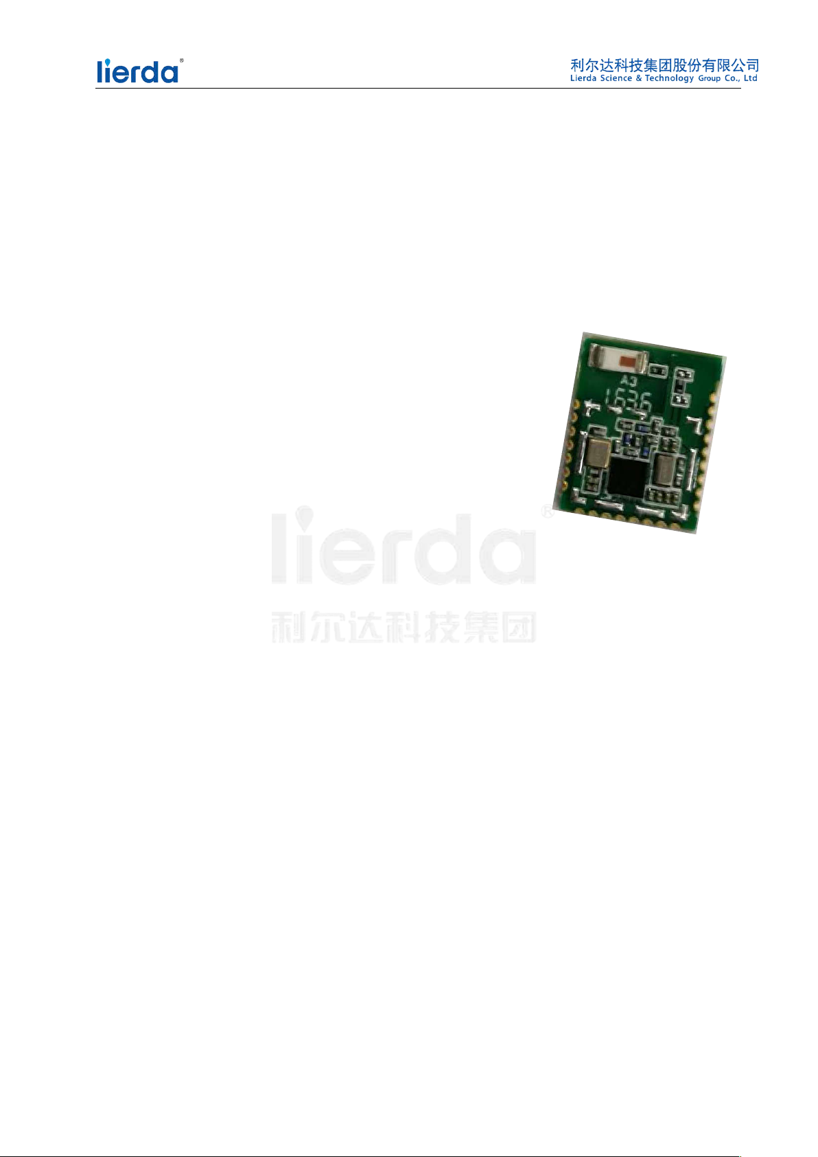
The low-power Bluetooth module is a high-performance Bluetooth SOC solution based on
ST's BLUENRG-134 chip, which is a compact, practical and convenient, high integration
module with stamp-type interface. The module provides a complete wireless solution and
perfect support for customers application development, saving the trouble of complicated RF
hardware design, development and production. With modular ceramic antenna, the product has
the feature of low power consumption, small size, anti-interference ability and etc..
High performance 32M and 32.768K Crystal
160K Flash /24-KB RAM
32-bit, ARM® Cortex®-M0
Support for 14 GPIOs
BLE SOC
13mm*10mm
5
Page 6
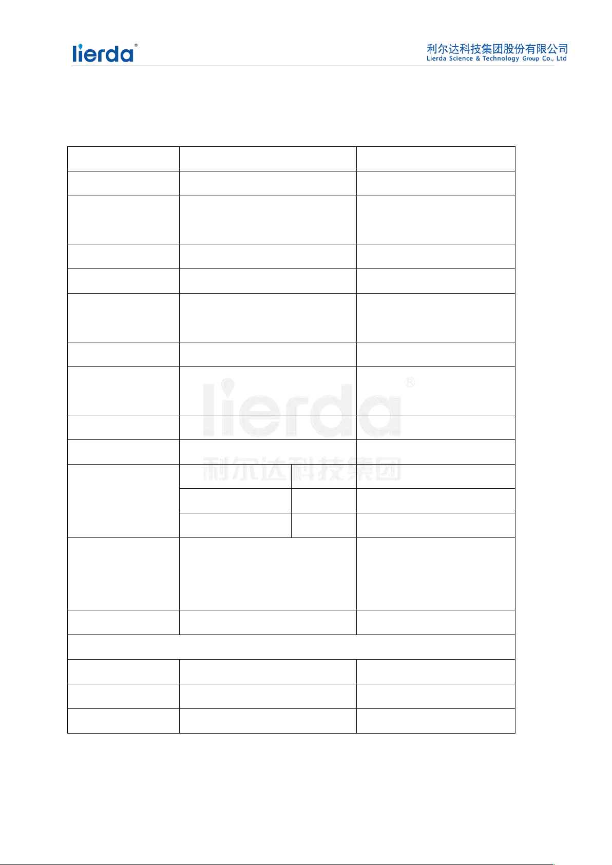
2 Specifications
Table1: Module Parameters
Parameters performance Note
Working voltage 1.7V~3.6V
Working
-40℃~85℃
temperature range
Frequency range 2400MHz~2483.5MHz
Modulation scheme GFSK
RF channel center
2402M--2480M(Ch0 -- Ch39) Channel spacing 2M
frequency
Tx Power 8--10dBm Typical value 9dBm
Tx current 8.6mA Typical value 8.6mA @3.3V
0 dBm
Rx current 8.1mA Typical value 8.1mA @3.3V
Sensitivity -84dBm
Sleep mode 0.9uA 32 kHz XO
Power consumption
Sleep mode 2.1uA 32 kHZ RO
Standby mode 500nA Standby
Transmission
>15m
See Notes
distance(Open area
and 0dBm)
Dimensions 13mm*10mm*2.3mm Length * width * height
Antenna
Antenna Type
Average Gain (XZ-V) -0.5 dBi typ Peak Gain 0.5 dBi typ
Dimensions ( L × W ) 3.2× 1.6 mm
Notes: "Transmission distance" is subject to surrounding environment, air humidity and other factors,
for reference only.
Multilayer Chip Antenna
6
Page 7
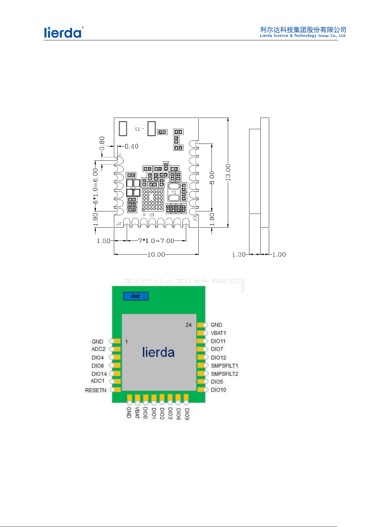
3 Hardware
3.1 Dimensions Diagram
Figure 1: Dimensions Diagram
Figure 2: Pin Diagram
7
Page 8
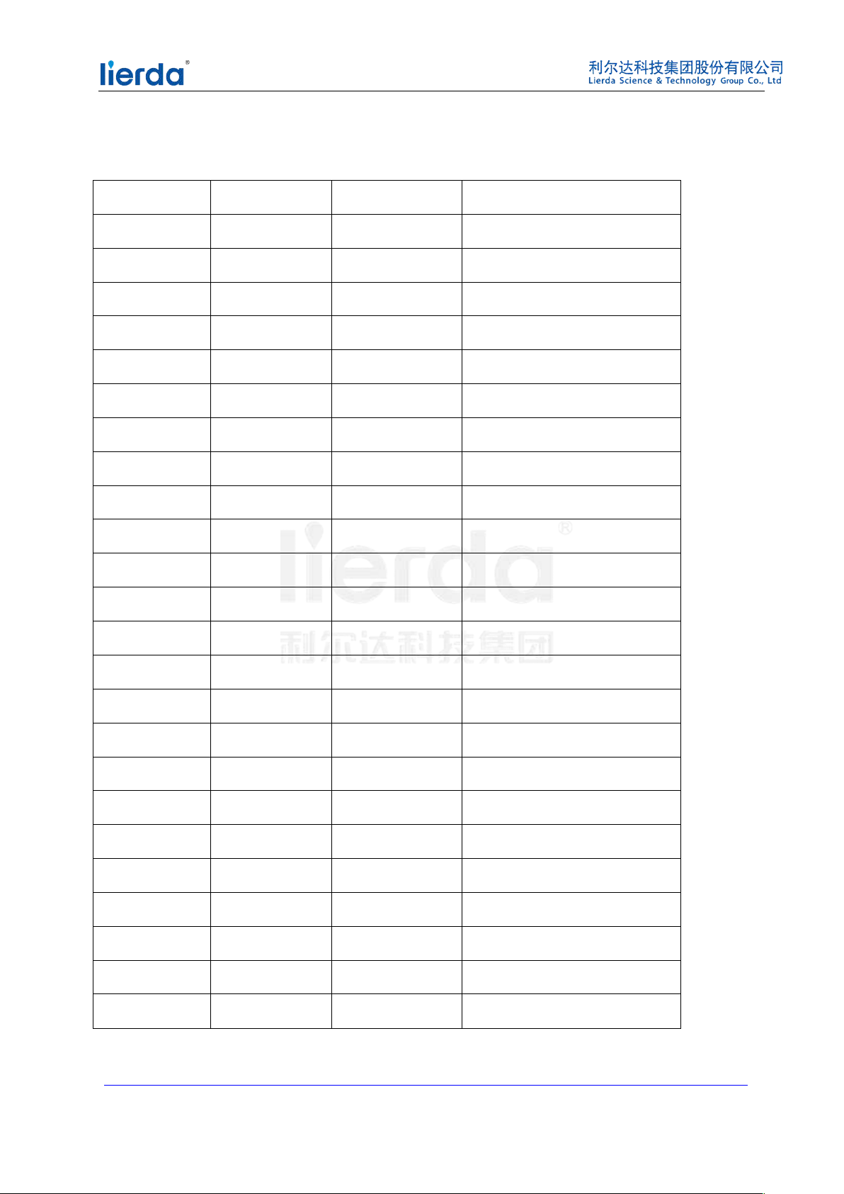
3.2 Pin Description
Pin Number Pin Name Type Description
1 GND Ground reference
2 ADC2 GPIO ADC2
3 DIO4 GPIO UART_RXD
4 DIO8 GPIO UART_TXD
5 DIO14 GPIO I2C1_CLK
6 ADC1 GPIO ADC1
7 RESETN Reset Pin
8 GND Ground reference
9 BAT1 Power 1.7~3.6V
10 DIO0 GPIO UART_CTS
11 DIO1 GPIO UART_RTS
12 DIO2 GPIO PWM0
13 DIO3 GPIO PWM1
14 DIO6 GPIO UART_RTS
15 DIO9 GPIO SWCLK
16 DIO10 GPIO SWDIO
17 DIO5 GPIO UART_TXD
18 SMPSFILT2 GPIO DC-DC
19 SMPSFILT1 GPIO DC-DC
20 DIO12 GPIO I2C1_CLK
21 DIO7 GPIO I2C2_DAT
22 DIO11 GPIO UART_RXD
23 BAT2 Power 1.7~3.6V
24 GND Ground reference
For more details, refer to BlueNRG-1DataSheet.
.http://www.st.com/content/ccc/resource/technical/document/datasheet/group3/ac/c1/ad/80/54/fa/49/9d/DM0
8
Page 9
0262983/files/DM00262983.pdf/jcr:content/translations/en.DM00262983.pdf
4 Applications
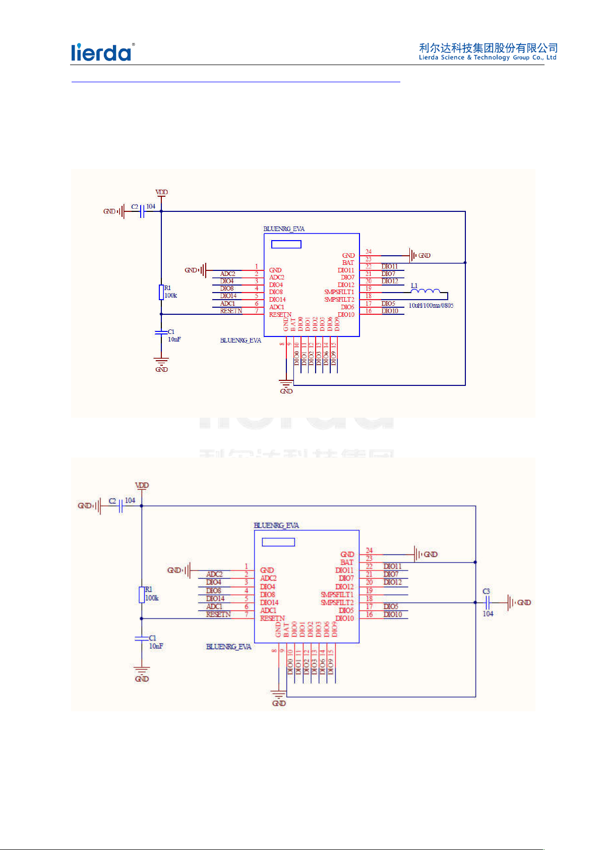
4.1 Application circuit
Active DC-DC Converter:
Figure 3: Application circuit: active DC-DC converter
Non-active DC-DC Converter:
Figure 4: Application circuit: non active DC-DC converter
Active DC-DC Converter will greatly reduce system power consumption, but will affect
9
Page 10
sensitivity of the system. Using an internal LDO increases sensitivity, but system power
consumption will be slightly higher.
4.2 Precautions
To ensure the module's RF performance in the application of its maximum possible
effectiveness, the user should follow the following principles:
1. It is recommended to supply the module with DC power supply. The power supply ripple
coefficient should be as small as possible. The module should be reliably grounded. Please pay
attention to the correct connection of positive and negative poles of the power supply. If the
connection is reversed, the module may be damaged permanently.
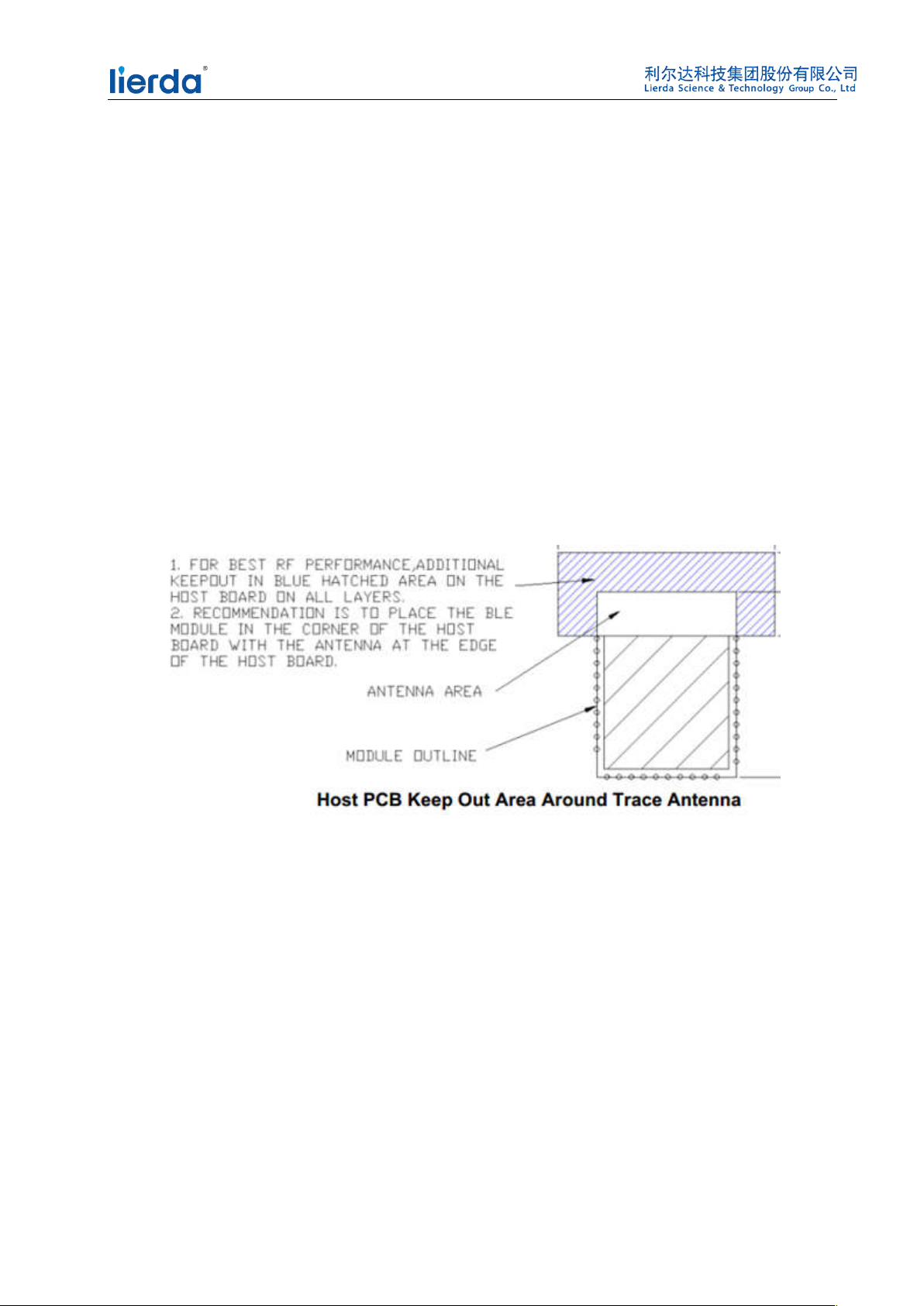
2. Module recommendations placed on the edge of the floor open space, the antenna should be
outward;
3. The module under the antenna PCB (double-sided board and multi-layer board) need
clearance, can not be deposited copper, that is all the layout layer below the antenna can not
have grounding or signal trace;
4. It is better to keep metal parts away from the antenna, or module communication distance in
different environments will be shortened at different degrees. Please refer to recommended
locations in following figure:
Figure4: Module recommended placement
4.3 Download and Debug
The module supports the ARM serial wire debug (SWD) port, the SWD port pin is
DIO9(SWCLK),DIO10(SWDIO).Through J-link or ST-LINK, you can download and debug.
When the module is power up or hardware reset, if DIO7 is high, you can enter the boot mode,
the module is not available at this time, the module can be programmed through the serial port
code.
4.4 Development board
Refer to LSD1RF-EVBGP001 data.
4.5 Reference manual
10
Page 11

BlueNRG-1_GATT_database_size.pdf
BlueNRG-1_Over_The_Air_Bootloader.pdf
BlueNRG-1_UART_bootloader_protocol.pdf
PM0257-BlueNRG-1 BLE stack programming guidelines.pdf
AN4820-BlueNRG-1 low power modes.p
5 Federal Communications Commission (FCC) Interference Statement
This equipment has been tested and found to comply with the limits for a Class C
digital device, pursuant to part 15 of the FCC Rules. These limits are designed to provide
reasonable protection against harmful interference in a residential installation. This
equipment generates, uses and can radiate radio frequency energy and, if not installed and
used in accordance with the instructions, may cause harmful interference to radio
communications. However, there is no guarantee that interference will not occur in a
particular installation. If this equipment does cause harmful interference to radio or
television reception, which can be determined by turning the equipment off and on, the user
is encouraged to try to correct the interference by one or more of the following measures:
—Reorient or relocate the receiving antenna.
—Increase the separation between the equipment and receiver.
—Connect the equipment into an outlet on a circuit different from that to which the
receiver is connected.
—Consult the dealer or an experienced radio/TV technician for help.
Note: Any changes or modifications not expressly approved by the party responsible for
compliance could void the user's authority to operate the equipment.
RF exposure warning
This equipment must be installed and operated in accordance with provided instructions
and the antenna(s) used for this transmitter must be installed to provide a separation
distance of at least 20 cm from all persons and must not be co-located or operating in
conjunction with any other antenna or transmitter. End-users and installers must be
provided with antenna installation instructions and transmitter operating conditions for
satisfying RF exposure compliance.
11
Page 12

Note
Welcome to use Lierda products, please read this notice before using our products. If you have
already used them, it means that you have read and accepted this notice.
Lierda reserves the right to interpret and modify all information contained herein without prior
notice.
Released by:Lierda MSBU
12
 Loading...