


Global LCD Panel Exchange Center |
www.panelook.com |
LC320W01
Liquid Crystal Display
Product Specification
SPECIFICATION
FOR
APPROVAL
( |
) |
Preliminary Specification |
|
|
|
|
||
( |
) |
Final Specification |
|
|
|
|
||
|
|
|
|
|
|
|
|
|
|
|
Title |
|
|
32.0” WXGA TFT LCD |
|||
|
|
|
|
|
|
|
|
|
|
|
BUYER |
|
General |
|
SUPPLIER |
LG.Philips LCD Co., Ltd. |
|
|
|
|
|
|
|
|
*MODEL |
LC320W01 |
|
|
MODEL |
|
|
|
|
||
|
|
|
|
|
|
|
||
|
|
|
|
|
|
|
MODEL |
SL01 |
|
|
|
|
|
|
|||
|
|
|
|
|
|
|
|
|
|
|
|
|
|
|
|
*When you obtain standard approval, |
|
|
|
|
|
|
|
|
please use the above model name without suffix |
|
APPROVED BY
 SIGNATURE


 DATE
DATE
/


 /
/ 
/
Please return 1 copy for your confirmation with your signature and comments.
APPROVED BY
SIGNATURE
DATE
Jay Yoon / G. Manager
REVIEWED BY
J.H.Park / Manager
PREPARED BY
B.J.Choi / Engineer
TV Product Development Dept.
LG. Philips LCD Co., Ltd
Ver. 0.0 |
Jun. 02, 2005 |
1 / 28 |
One step solution for LCD / PDP / OLED panel application: Datasheet, inventory and accessory! www.panelook.com

Global LCD Panel Exchange Center |
www.panelook.com |
LC320W01
Liquid Crystal Display
Product Specification
CONTENTS
Number |
ITEM |
Page |
|
|
|
|
COVER |
1 |
|
CONTENTS |
2 |
|
RECORD OF REVISIONS |
3 |
1 |
GENERAL DESCRIPTION |
4 |
2 |
ABSOLUTE MAXIMUM RATINGS |
5 |
3 |
ELECTRICAL SPECIFICATIONS |
6 |
3-1 |
ELECTRICAL CHARACTERISTICS |
6 |
3-2 |
INTERFACE CONNECTIONS |
8 |
3-3 |
SIGNAL TIMING SPECIFICATIONS |
12 |
3-4 |
SIGNAL TIMING WAVEFORMS |
13 |
3-5 |
COLOR INPUT DATA REFERENCE |
14 |
3-6 |
POWER SEQUENCE |
15 |
4 |
OPTICAL SPECIFICATIONS |
17 |
5 |
MECHANICAL CHARACTERISTICS |
21 |
6 |
RELIABILITY |
24 |
7 |
INTERNATIONAL STANDARDS |
25 |
7-1 |
SAFETY |
25 |
7-2 |
EMC |
25 |
8 |
PACKING |
26 |
8-1 |
DESIGNATION OF LOT MARK |
26 |
8-2 |
PACKING FORM |
26 |
9 |
PRECAUTIONS |
27 |
9-1 |
MOUNTING PRECAUTIONS |
27 |
9-2 |
OPERATING PRECAUTIONS |
27 |
9-3 |
ELECTROSTATIC DISCHARGE CONTROL |
28 |
9-4 |
PRECAUTIONS FOR STRONG LIGHT EXPOSURE |
28 |
9-5 |
STORAGE |
28 |
9-6 |
HANDLING PRECAUTIONS FOR PROTECTION FILM |
28 |
|
|
|
|
|
|
Ver. 0.0 |
Jun. 02, 2005 |
2 / 28 |
One step solution for LCD / PDP / OLED panel application: Datasheet, inventory and accessory! www.panelook.com

Global LCD Panel Exchange Center |
www.panelook.com |
LC320W01
Liquid Crystal Display
Product Specification
RECORD OF REVISIONS
Revision No |
Revision Date |
Page |
|
Description |
0.0 |
Jun. 02, 2005 |
- |
Preliminary Specification |
|
Ver. 0.0 |
|
|
Jun. 02, 2005 |
3 / 28 |
One step solution for LCD / PDP / OLED panel application: Datasheet, inventory and accessory! www.panelook.com

Global LCD Panel Exchange Center |
www.panelook.com |
LC320W01
Liquid Crystal Display
Product Specification
1. General Description
The LC320W01 is a Color Active Matrix Liquid Crystal Display with an integral External Electrode Fluorescent Lamp(EEFL) backlight system. The matrix employs a-Si Thin Film Transistor as the active element. It is a transmissive type display operating in the normally black mode. It has a 31.51 inch diagonally measured active display area with WXGA resolution (768 vertical by 1366 horizontal pixel array). Each pixel is divided into Red, Green and Blue sub-pixels or dots which are arranged in vertical stripes. Gray scale or the luminance of the sub-pixel color is determined with a 8-bit gray scale signal for each dot, thus presenting a palette of more than 16.7M(true) colors. 


It has been designed to apply the 8-bit 1-port LVDS interface.
It is intended to support LCD TV, PCTV where high brightness, super wide viewing angle, high color gamut, high color depth and fast response time are important. 


|
|
|
|
|
RGB(Mini-LVDS) |
Source Driver Circuit |
|
|
|
CN4 |
LUT Data |
LUT Data |
|
||
|
|
|
S1 |
S1366 |
|||
+12.0V |
|
|
DCR LUT, |
ODC LUT |
|
||
|
|
|
G1 |
|
|||
LVDS |
|
|
Gate |
|
|||
|
|
|
|
|
|
||
5pair |
|
|
|
|
|
|
|
|
|
|
|
|
|
|
|
Select |
#9 |
CN1 |
LVDS Rx (Receiver) |
Driver |
|
TFT - LCD Panel |
|
Enable |
#10 (30pin) |
DCR Controller |
|
||||
|
|
||||||
VBR_EXT |
#28 |
|
ODC Controller |
Circuit |
G768 |
(1366 Ý RGB Ý 768 pixels) |
|
VBR_OUT |
#27 |
|
Timing Controller |
|
|||
|
|
|
|
||||
|
|
|
Power Circuit |
|
|
|
|
|
|
|
Block |
|
|
|
|
|
+24.0V |
|
|
CN2, Inverter (Master, 12Pin, High) |
|
Back light Assembly (18EEFL) |
|
|
+24.0V |
|
|
|
|||
|
|
|
|
|
|||
|
|
CN3, Inverter (Slaver, 12Pin, High) |
|
|
|
||
|
|
|
|
|
|
|
|
|
|
|
|
|
|
||
|
|
|
|
|
|
|
|
General Features |
|
|
|
|
|||
Active Screen Size |
31.51 inches(800.4mm) diagonal |
|
|
|
|
Outline Dimension |
760.0 mm(H) x 450.0 mm(V) x 48.0 mm(D) (Typ.) |
|
|
|
|
Pixel Pitch |
170.25 x 510.75 x RGB |
|
|
|
|
Pixel Format |
1366 horiz. by 768 vert. pixels RGB stripe arrangement |
|
Color Depth |
8bit, 16,7 M colors |
|
Luminance, White |
500 cd/m2 (Center 1 point) (Typ.) |
|
Dynamic C/R (for AI) |
1600:1 (Typ.) |
|
Viewing Angle (CR>10) |
Viewing angle free ( R/L 178(Typ.), U/D 178(Typ.)) |
|
Power Consumption |
Total 88.86 Watt (Typ.) (Logic=4.86 W, Lamp=84W [IBL=90mA] ) |
|
Weight |
6,900 g (Typ.) |
|
Display Operating Mode |
Transmissive mode, normally black |
|
Surface Treatment |
Hard coating(3H), anti-glare treatment of the front polarizer |
|
|
|
|
|
|
|
Ver. 0.0 |
Jun. 02, 2005 |
4 / 28 |
One step solution for LCD / PDP / OLED panel application: Datasheet, inventory and accessory! www.panelook.com

Global LCD Panel Exchange Center |
www.panelook.com |
LC320W01
Liquid Crystal Display
Product Specification
2. Absolute Maximum Ratings
The following items are maximum values which, if exceeded, may cause faulty operation or damage to the LCD module.
Table 1. ABSOLUTE MAXIMUM RATINGS
Parameter |
Symbol |
|
Value |
Unit |
Remark |
||
|
|
|
|||||
Min |
|
Max |
|||||
|
|
|
|
|
|
||
|
|
|
|
|
|
|
|
Power Input |
LCM |
VLCD |
-0.3 |
|
+14.0 |
VDC |
GY\G YG¶j |
Voltage |
Backlight inverter |
VBL |
21.6 |
|
+27.0 |
VDC |
|
|
|
|
|
|
|
|
|
ON/OFF Control Voltage |
VON/OFF |
-0.3 |
|
+5.25 |
VDC |
|
|
Brightness Control Voltage |
VBr |
0 |
|
+5.0 |
VDC |
|
|
Operating Temperature |
TOP |
0 |
|
+40 |
¶C |
|
|
Storage Temperature |
TST |
-20 |
|
+50 |
¶C |
Note 1 |
|
Operating Ambient Humidity |
HOP |
10 |
|
90 |
%RH |
||
|
|
||||||
Storage Humidity |
HST |
10 |
|
90 |
%RH |
|
|
|
|
|
|
|
|
|
|
Note : 1. Temperature and relative humidity range are shown in the figure below. Wet bulb temperature should be 39 ¶C Max. and no condensation of water.
|
|
|
|
|
|
|
|
ڔڋڀ |
|
|
|
|
|
|
|
|
|
|
ڑڋ |
|
|
|
|
|
|
|
|
|
|
|
|
|
ڑڋڀ |
|
|
|
Wet Bulb |
|
|
|
ڐڋ |
|
|
|
ڣېۈۄڿۄۏ۔ٻڶڃڀڄڭڣڸ |
ڮۏۊۍڼۂۀ |
|
|
|
|
|
|
|
|
|
|
|||
|
|
|
|
|
|
|
|
|
|
||
|
Temperature [ |
] |
ڏڋ |
|
|
|
|
|
|
||
|
|
|
|
|
|
|
|
|
|
|
|
|
|
|
|
|
|
|
|
|
ڏڋڀ |
|
ڪۋۀۍڼۏۄۊۉ |
|
|
|
|
ڎڋ |
|
|
|
|
|
|
|
|
|
|
|
|
|
|
|
|
|
|
|
|
|
|
ڍڋ |
|
|
|
|
|
|
|
|
|
|
ڌڋ |
|
|
|
|
|
|
|
|
|
|
ڋ |
|
|
|
|
|
|
|
ڌڋڀ |
|
|
|
|
|
|
|
|
|
|
|
|
|
|
ڈڍڋ |
ڋ |
ڌڋ |
ڍڋ |
ڎڋ |
ڏڋ |
ڐڋ |
ڑڋ |
ڒڋ |
ړڋ |
|
|
Dry Bulb Temperature [¶C]
Ver. 0.0 |
Jun. 02, 2005 |
5 / 28 |
One step solution for LCD / PDP / OLED panel application: Datasheet, inventory and accessory! www.panelook.com

Global LCD Panel Exchange Center |
www.panelook.com |
LC320W01
Liquid Crystal Display
Product Specification
3. Electrical Specifications
3-1. Electrical Characteristics
It requires two power inputs. One is employed to power for the LCD circuit. The other input power for the EEFL/Backlight is to power inverter. 


Table 2-1. ELECTRICAL CHARACTERISTICS
Parameter |
Symbol |
|
Value |
|
|
Unit |
Note |
|
|
|
|
||||
Min |
Typ |
Max |
|
||||
|
|
|
|
|
|||
|
|
|
|
|
|
|
|
MODULE : |
|
|
|
|
|
|
|
|
|
|
|
|
|
|
|
Power Input Voltage |
VLCD |
11.4 |
12.0 |
12.6 |
|
VDC |
|
Permissible Input Ripple Voltage |
VRP |
- |
- |
200 |
|
mVP-P |
|
Power Input Current |
ILCD |
- |
405 |
527 |
|
mA |
1 |
- |
520 |
676 |
|
mA |
2 |
||
|
|
|
|||||
Power Consumption |
PLCD |
- |
4.86 |
6.33 |
|
Watt |
1 |
|
|
|
|
|
|
|
|
Rush current |
IRUSH |
- |
- |
3.0 |
|
A |
3 |
|
|
|
|
|
|
|
|
Notes : 1. The specified current and power consumption are under the VLCD=12.0V, 25 2¶C, fV=60Hz condition whereas mosaic pattern(8 x 6) is displayed and fV is the frame frequency.
2.The current is specified at the maximum current pattern.
3.The duration of rush current is about 2ms and rising time of power input is 1ms (min.).
White : 255Gray
Black : 0Gray
Mosaic Pattern(8 x 6)
Ver. 0.0 |
Jun. 02, 2005 |
6 / 28 |
One step solution for LCD / PDP / OLED panel application: Datasheet, inventory and accessory! www.panelook.com

Global LCD Panel Exchange Center |
www.panelook.com |
LC320W01
Liquid Crystal Display
Product Specification
Table 2-2. ELECTRICAL CHARACTERISTICS
Parameter |
|
Symbol |
|
Value |
|
Unit |
Note |
|
|
Min |
Typ |
Max |
|||||
|
|
|
|
|
|
|||
Inverter : |
|
|
|
|
|
|
|
|
Power Input Voltage |
|
|
VBL |
22.8 |
24.0 |
25.2 |
VDC |
1 |
Power Input Current |
|
|
IBL |
- |
3.5 |
3.85 |
A |
1 |
Power Consumption |
|
|
PBL |
- |
84 |
92.4 |
W |
1 |
Brightness |
Adjust |
VBR |
0 |
|
3.3 |
VDC |
2 |
|
Input Voltage for |
|
|
|
|
|
|
|
|
Control System |
On/Off |
On |
V on |
3.0 |
5.0 |
5.25 |
VDC |
|
Signals |
Off |
V off |
-0.3 |
0 |
0.8 |
VDC |
|
|
|
|
|
||||||
Lamp : |
|
|
|
|
|
|
|
|
Life Time |
|
25·2 |
|
50,000 |
|
|
Hrs |
3 |
Note : 1. The specified current and power consumption are under the typical supply Input voltage, 24.0V. Ripple voltage of the Power Input Voltage is under 0.2 Vp-p.
2. Brightness Control.
This VBR Voltage control brightness.
VBR Voltage |
Function |
|
|
3.3V |
Maximum Brightness (100%) |
|
|
0V |
Minimum Brightness.(30%) |
|
|
3. Specified values are for a single lamp which is aligned horizontally.
 The Life Time is determined as the time at which brightness of the lamp is 50% compared to that of

 initial value at the typical lamp current on condition of continuous operating at each ambient


 temperature.
Ver. 0.0 |
Jun. 02, 2005 |
7 / 28 |
One step solution for LCD / PDP / OLED panel application: Datasheet, inventory and accessory! www.panelook.com

Global LCD Panel Exchange Center |
www.panelook.com |
LC320W01
Liquid Crystal Display
Product Specification
3-2. Interface Connections
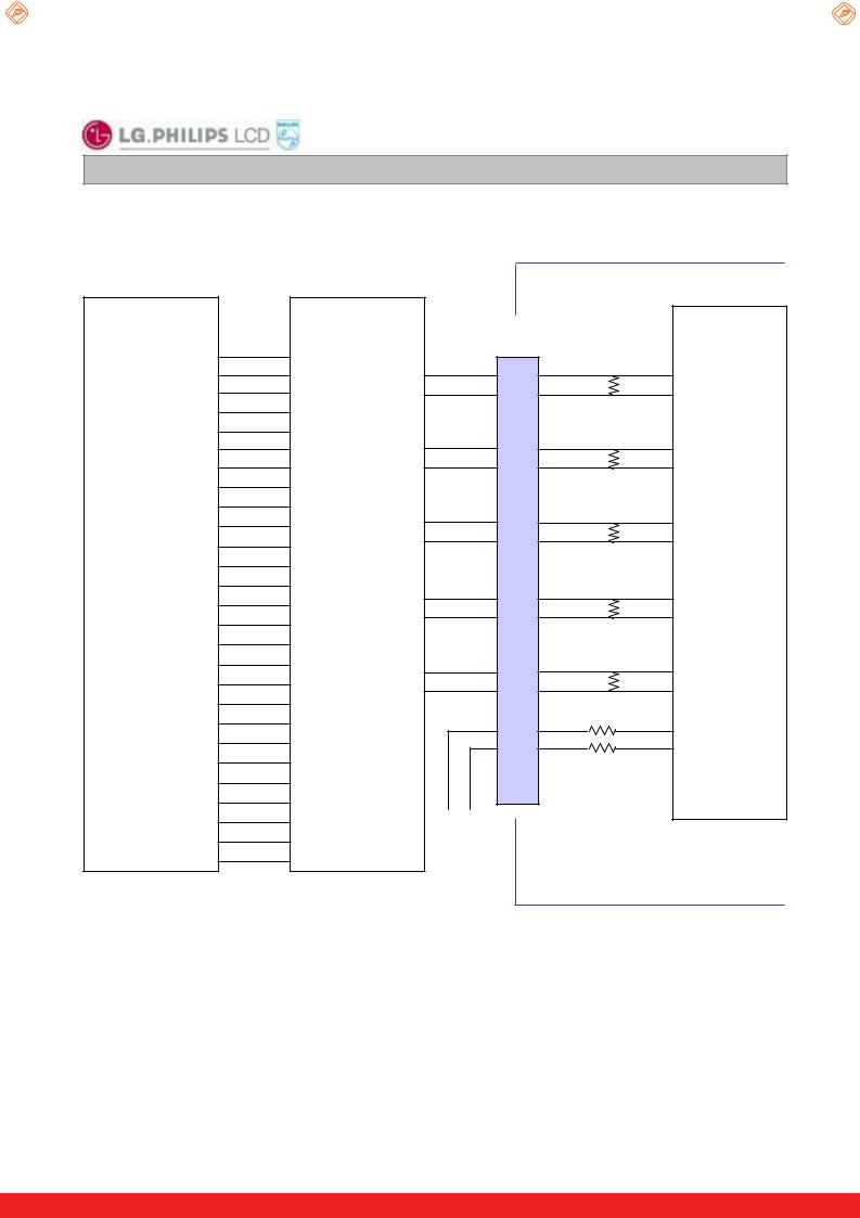
This LCD module employs two kinds of interface connection, a 30-pin connector is used for the module electronics and two 12-pin connectors are used for the integral backlight system.
3-2-1. LCD Module
- LCD Connector(CN1) : FI-X30SSL-HF (Manufactured by JAE) or Equivalent - Mating Connector : FI-30C2L (Manufactured by JAE) or Equivalent
Table 3. MODULE CONNECTOR(CN1) PIN CONFIGURATION
Pin No. |
Symbol |
Description |
Note |
1 |
VLCD |
Power Supply +12.0V |
|
2 |
VLCD |
Power Supply +12.0V |
|
3 |
VLCD |
Power Supply +12.0V |
|
4 |
VLCD |
Power Supply +12.0V |
|
5 |
GND |
Ground |
|
6 |
GND |
Ground |
|
7 |
GND |
Ground |
|
8 |
GND |
Ground |
|
9 |
Select |
Select LVDS Data format |
1 |
10 |
kjyGl |
k GjyGl GOG‘sG Guj’dGk GSG‘o’ dGl GP |
2 |
11 |
GND |
Ground |
|
12 |
RA- |
LVDS Receiver Signal(-) |
|
13 |
RA+ |
LVDS Receiver Signal(+) |
|
14 |
GND |
Ground |
|
15 |
RB- |
LVDS Receiver Signal(-) |
|
16 |
RB+ |
LVDS Receiver Signal(+) |
|
17 |
GND |
Ground |
|
18 |
RC- |
LVDS Receiver Signal(-) |
|
19 |
RC+ |
LVDS Receiver Signal(+) |
|
20 |
GND |
Ground |
|
21 |
RCLK- |
LVDS Receiver Clock Signal(-) |
|
22 |
RCLK+ |
LVDS Receiver Clock Signal(+) |
|
23 |
GND |
Ground |
|
24 |
RD- |
LVDS Receiver Signal(-) |
|
25 |
RD+ |
LVDS Receiver Signal(+) |
|
26 |
GND |
Ground |
|
27 |
}iy v|{ |
}iyG G GsjkG |
|
28 |
}iy l { |
l G}iyG G Gz G GsjkG |
|
29 |
GND |
Ground |
|
30 |
GND |
Ground |
3 |
Note: 1. If the pin no. 9 is Ground, Interface format is “LG”, and if the pin no. 9 is Vcc(3.3V), Interface format

 is “DISM”. See page 9 and 10.
 2. When #10 pin is no connection, DCR is disabled.
3. The pin no. 30 is necessary for LCD test.
When LVDS signals are abnormal operation more than 3-Vsync times and power 12V is supplied, ‘Open’ or ‘Vcc’ : LCD operate itself some test patterns.(AGP – Auto Generation Pattern)
‘Ground’ : LCD operate itself a black pattern. (NSB – No Signal Black) LPL recommend ‘Ground’ for NSB.
4.All GND (ground) pins should be connected together, which should be also connected to the LCD module’s metal frame.
5.All VLCD (power input) pins should be connected together.
6.Input Levels of LVDS signals are based on the IEA 664 Standard.
Ver. 0.0 |
Jun. 02, 2005 |
8 / 28 |
One step solution for LCD / PDP / OLED panel application: Datasheet, inventory and accessory! www.panelook.com
Global LCD Panel Exchange Center |
www.panelook.com |
LC320W01
Liquid Crystal Display
Product Specification
Table 4. REQUIRED SIGNAL ASSIGNMENT FOR LVDS TRANSMITTER ( Pin9=“L” or “Open” )
Host System |
|
DS90C385 |
|
|
|
Timing |
|
24 Bit |
|
or Compatible |
|
|
|
||
|
|
FI-X30SSL-HF |
|
Controller |
|||
RED0 |
51 |
|
48 |
|
|
|
|
RED1 |
52 |
TxOUT0- |
12 |
|
RxIN0- |
||
47 |
100˟ |
||||||
RED2 |
54 |
TxOUT0+ |
13 |
RxIN0+ |
|||
|
|
||||||
RED3 |
55 |
|
|
|
|
|
|
RED4 |
56 |
|
46 |
|
|
|
|
RED5 |
3 |
TxOUT1- |
15 |
|
RxIN1- |
||
45 |
100˟ |
||||||
RED6 |
50 |
TxOUT1+ |
16 |
RxIN1+ |
|||
|
|
||||||
RED7 |
2 |
|
|
|
|
|
|
GREEN0 |
4 |
|
42 |
|
|
|
|
GREEN1 |
6 |
TxOUT2- |
18 |
|
RxIN2- |
||
41 |
100˟ |
||||||
GREEN2 |
7 |
TxOUT2+ |
19 |
RxIN2+ |
|||
|
|
||||||
GREEN3 |
11 |
|
|
|
|
|
|
GREEN4 |
12 |
|
40 |
|
|
|
|
GREEN5 |
14 |
TxCLKOUT- |
21 |
|
RxCLKIN- |
||
39 |
100˟ |
||||||
GREEN6 |
8 |
TxCLKOUT+ |
22 |
RxCLKIN+ |
|||
|
|
||||||
GREEN7 |
10 |
|
|
|
|
|
|
BLUE0 |
15 |
|
38 |
|
|
|
|
BLUE1 |
19 |
TxOUT3- |
24 |
|
RxIN3- |
||
37 |
100˟ |
||||||
BLUE2 |
20 |
TxOUT3+ |
25 |
RxIN3+ |
|||
|
|
||||||
BLUE3 |
22 |
|
|
|
|
|
|
BLUE4 |
23 |
|
|
9 |
|
LG / DISM |
|
BLUE5 |
24 |
|
|
30 |
|
LCD Test |
|
BLUE6 |
16 |
|
|
|
|
|
|
BLUE7 |
18 |
|
|
|
|
|
|
Hsync |
27 |
|
GND |
GND |
|
|
|
Vsync |
28 |
|
|
|
|||
Data Enable |
30 |
|
|
LCD Module |
|||
CLOCK |
31 |
|
|
|
|
||
|
|
|
|
|
Note: 1. The LCD Module uses a 100 Ohm [ȳ] resistor between positive and negative lines of each receiver input.
2.Refer to LVDS Transmitter Data Sheet for detail descriptions. (DS90C385 or Compatible)
3.‘7’ means MSB and ‘0’ means LSB at R,G,B pixel data.
Ver. 0.0 |
Jun. 02, 2005 |
9 / 28 |
One step solution for LCD / PDP / OLED panel application: Datasheet, inventory and accessory! www.panelook.com
 Loading...