


LC200WX1
Liquid Crystal Display
Product Specification
SPECIFICATION
FOR
APPROVAL
)
(
(
Preliminary Specification
)
Final Specification
●
Title 20.0” WXGA TFT LCD
BUYER General
MODEL -
www.jxlcd.com
www.jxlcd.com
APPROVED BY
/
/
/
SIGNATURE
DATE
SUPPLIER LG.Philips LCD Co., Ltd.
*MODEL LC200WX1
SUFFIX SLB2
*When you obtain standard approval,
please use the above model name without suffix
APPROVED BY
J.H Yoon / Senior Manager
REVIEWED BY
H.I Jang / Manager
PREPARED BY
D.W Lee / Engineer
SIGNATURE
DATE
Please return 1 copy for your confirmation with
your signature and comments.
Ver. 0.0 Jan.17, 2006
TV Product Development Dept.
LG. Philips LCD Co., Ltd
1/ 28
LC200WX1
Liquid Crystal Display
Product Specification
Contents
Number ITEM Page
COVER
CONTENTS
RECORD OF REVISIONS 3
1 GENERAL DESCRIPTION
2 ABSOLUTE MAXIMUM RATINGS
3 ELECTRICAL SPECIFICATIONS
3-1 ELECTRICAL CHARACTERISTICS
3-2 INTERFACE CONNECTIONS
3-3 SIGNAL TIMING SPECIFICATIONS
3-4 SIGNAL TIMING WAVEFORMS
3-5 COLOR INPUT DATA REFERENCE
3-6 POWER SEQUENCE
4 OPTICAL SPECIFICATIONS
5 MECHANICAL CHARACTERISTICS
6 RELIABILITY
www.jxlcd.com
www.jxlcd.com
1
2
4
5
6
6
8
12
13
14
15
17
21
24
7 INTERNATIONAL STANDARDS
7-1 SAFETY
7-2 EMC
8 PACKING
8-1 DESIGNATION OF LOT MARK
8-2 PACKING FORM
9 PRECAUTIONS 27
9-1 MOUNTING PRECAUTIONS 27
9-2 OPERATING PRECAUTIONS 27
9-3 ELECTROSTATIC DISCHARGE CONTROL 28
9-4 PRECAUTIONS FOR STRONG LIGHT EXPOSURE 28
9-5 STORAGE 28
9-6 HANDLING PRECAUTIONS FOR PROTECTION FILM 28
Ver. 0.0 Jan.17, 2006
25
25
25
26
26
26
2/ 28
Product Specification
Record of Revisions
Revision No. Revision Date Page Description
0.0
Jan.16,2006
-
Preliminary Specification(First Draft)
LC200WX1
Liquid Crystal Display
www.jxlcd.com
www.jxlcd.com
Ver. 0.0 Jan.17, 2006
3/ 28
LC200WX1
Liquid Crystal Display
Product Specification
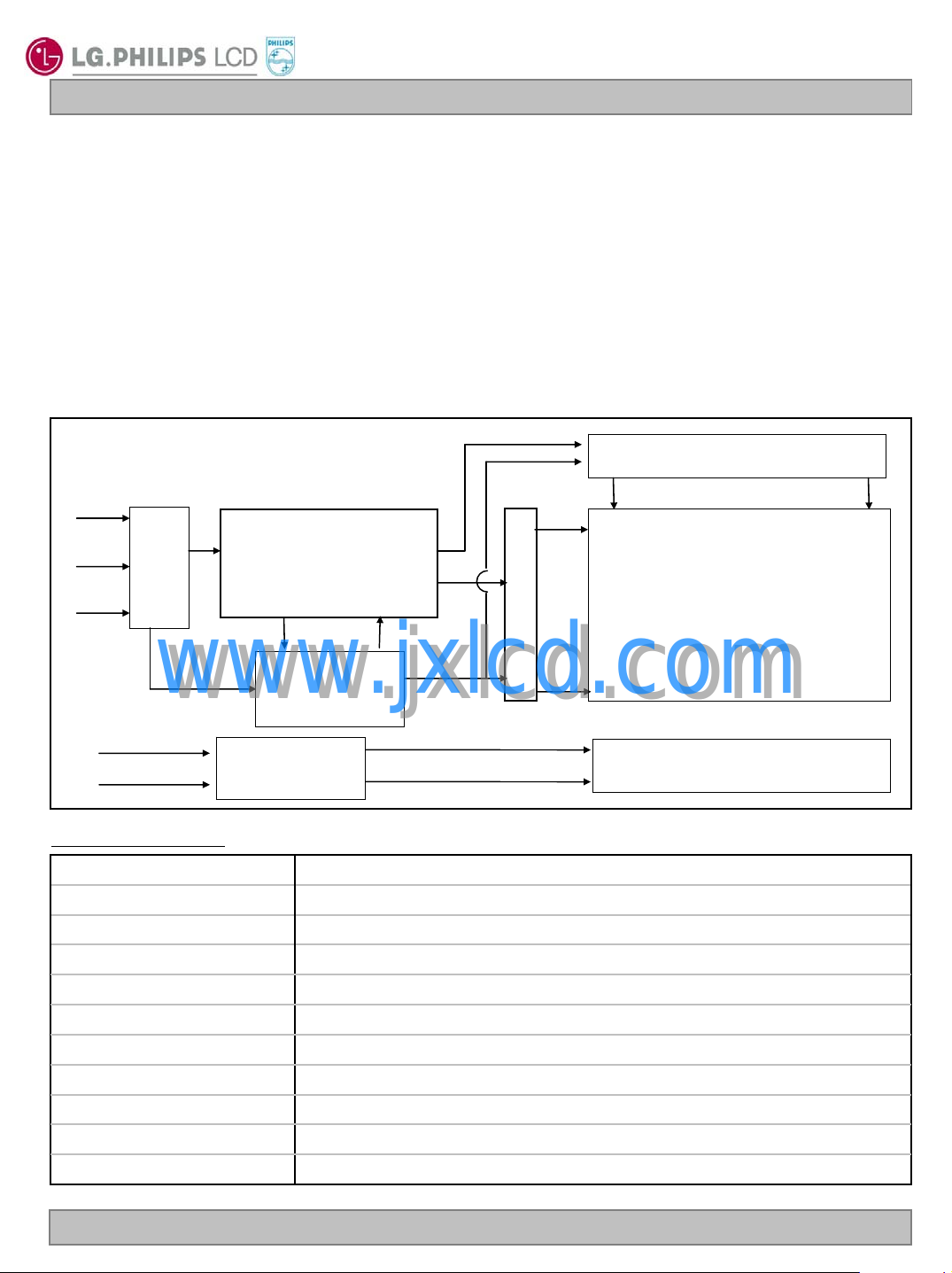
1. General Description
LC200WX1-SLB2 is a Color Active Matrix Liquid Crysta l Display with an integral Cold Cathode Fluorescent
Lamp(UCCFL) backlight system. The matrix employs a-Si Thin Film Transistor as the active element.
It is a transmissive type display operating in the normally black mode. It has a 20.04 inch diagonally
measured active display area with WXGA resolution (768 vertical by 1366 horizontal pixel array)
Each pixel is divided into Red, Green and Blue sub-pixels or dots which are arranged in vertical stripes.
Gray scale or the luminance of the sub-pixe l color is determined with a 8-bit gray scale signal fo r each dot,
thus presenting a palette of more than 16.7M(true) colors.
It has been designed to apply the 8-bit 1 port LVDS interface.
It is intended to support LCD TV, PCTV where high brightness, super wide view ing angle, high color gamut,
high color depth and fast response time are important.
RGB
Source Driver Circuit
S1 S1366
G1
+12.0V
LVDS
5pair
Option
# 9,28
CN1
(30pin)
Timing Controller
(LVDS Rx integrated)
Gate Driver Circuit
TFT - LCD Panel
(1366 × RGB × 768 pixels)
www.jxlcd.com
www.jxlcd.com
+24.0V
GND
Power Circuit
Block
Inverter
(CN2,14pin)
G768
General Features
Active Screen Size 20.04 inches (509.016mm) diagonal
Outline Dimension 472.0mm(H) x 275.0mm(V) x 38.0mm(D) (Typ.)
Pixel Pitch
Pixel Format
Color Depth
Luminance, White
Viewing Angle (CR>10)
Power Consumption
Weight
Display Operating Mode
Surface Treatment
0.108mm x 0.324mm x RGB
1366 horiz. by 768 vert. pixels RGB stripe arrangement
8-bit, 16.7 M colors
430 cd/m2 (Center 1 point Typ.)
Viewing angle free ( R/L 178(Typ.), U/D 178(Typ.))
Total 54.00Watt (Typ.) (Logic=3.00W, Backlight=51.0W )
2,800 g (Typ.), 3,000 g (Max)
Transmissive mode, normally black
Hard coating(3H), Anti-glare treatment of the front polarizer
Back light Assembly (5UCCFL)
Ver. 0.0 Jan.17, 2006
4/ 28
LC200WX1
Liquid Crystal Display
Product Specification
2. Absolute Maximum Ratings
The followings are maximum values which, if exceeded, may cause faulty operation or damage to the unit.
Table 1. ABSOLUTE MAXIMUM RATINGS
Parameter
Power Input
Voltage
ON/OFF Control Voltage VON/OFF -0.30 5.25 VDC
Brightness Control Voltage Vbr-A 0.0 5.25 VDC
Operating Temperature TOP 0 40
Storage Temperature TST -20 50
Operating Ambient Humidity HOP 10 90 %RH
Storage Humidity HST 10 90 %RH
Notes : 1. Temperature and relative humidity range are shown in the figure below.
LCM
Backlight inverter VBL -0.3 27.0 VDC
Wet bulb temperature should be 39 °C Max, and no condensation of water.
www.jxlcd.com
www.jxlcd.com
VLCD -0.3 14.0 VDC at 25 ± 2 °C
Value
Unit
Min Max
℃
℃
90%
60
60%
RemarkSymbol
Note 1
Wet Bulb
50
Temperature [℃]
40
30
20
10
0
10 20 30 40 50 60 70 800-20
Dry Bulb Temperature [°C]
Figure 2. Temperature a nd relative humidity
Ver. 0.0 Jan.17, 2006
40%
10%
Storage
Operation
Humidity [(%)RH]
5/ 28
LC200WX1
Liquid Crystal Display
Product Specification
3. Electrical Specifications 3-1. Electrical Characteristics
It requires two power inputs. One is employed to power the LCD electronics and to drive the TFT array and
liquid crystal. The other input power for th e UCCFL/Backlight is to power inverter.
Table 2_1. ELECTRICAL CHARACTERISTICS
Parameter Symbol
Min Typ Max
MODULE :
Power Input Voltage VLCD
Power Input Current ILCD
Power Consumption PLCD
Rush current IRUSH
Note :
1. The specified current and power consumption are under the V
whereas mosaic pattern(8 x 6) is displayed and f
2. The current is specified at the maximum current pattern.
3. The duration of rush current is about 2ms and rising time of power Input is 1ms(min.).
www.jxlcd.com
www.jxlcd.com
White : 255Gray
Black : 0Gray
11.4 12.0 12.6
- 250 325
- 340 442
- 3.00 3.90
- - 3.0
is the frame frequency.
V
Value
=12.0V, 25 ± 2°C, fV=60Hz condition
LCD
Unit Note
VDC
mA 1
mA 2
Watt 1
A 3
Mosaic Pattern(8 x 6)
Ver. 0.0 Jan.17, 2006
6/ 28
Product Specification
Table 3. Inverter Electrical Characteristics
LC200WX1
Liquid Crystal Display
Parameter Symbol Condition
Input Voltage V
Input Current I
Inrush Current
Power Consumption
B/L on/off control
Brightness Adj
(Analog mode)
Brightness Adj
(Burst mode)
Frequency (PWM)
(Burst mode)
Pulse Duty(PWM)
(Burst mode)
Lamp Life Time 50,000 60,000 Hrs 2
www.jxlcd.com
www.jxlcd.com
BL
BL
I
RUSH
P
BL
V
ON/OFF
VBR-A 0 - 3.3 V
EXTVBR-B
f-B
VBR-A(max) = 3.3V 1.8 2.125 2.4 A
VBL=21.6V
V
-A=3.3V
BR
EXTV
VBR–A =3.3V - 51 57.6 Watt 1, 3
Lamp ON = High 2.4 - 5.0 V
Lamp OFF =Low 0.0 0.6 V
External Input
(PWM)
VBL=24V
EXTV
High Level 2.5 - 5.0 V
Low Level 0.0 - 0.6 V
-B=100%
BR
-B=PWM
BR
Min. Typ. Max.
21.6 24.0 25.2 V
- - 3.0 A 5
20 - 100 % 4
- 180 - Hz 6
Value
Unit
DC
DC
DC
DC
DC
DC
Note
1, 3
Notes :
1. The specified current and power consumption are under the typical supply Input voltage, 24.0V.
The ripple voltage of the power supply input voltage is under 0.5 Vp-p.
Inrush current of the power supply input current is under +10% of the typical current
2. Specified values are for a single lamp which is aligned horizontally.
The life is determined as the time at which luminance of the lamp is 50% compared to that of initial
value at the typical lamp current on condition of continuous operating at 25 ± 2°C.
Specified value is when lamp is aligned horizontally.
3. Electrical characteristics are determined after the unit has been ‘ON’ and stable for approximately
2Hrs in a dark environment at 25 °C± 2°C.
4. Burst mode is controlled by TV system.
5. Rush current is determined at turning on after the unit has been ‘OFF’ for 2Hrs at 25 °C± 2°C.
6. Synchronize PWM by triple with Vsync signal of system.
Ver. 0.0 Jan.17, 2006
7/ 28

LC200WX1
Liquid Crystal Display
Product Specification
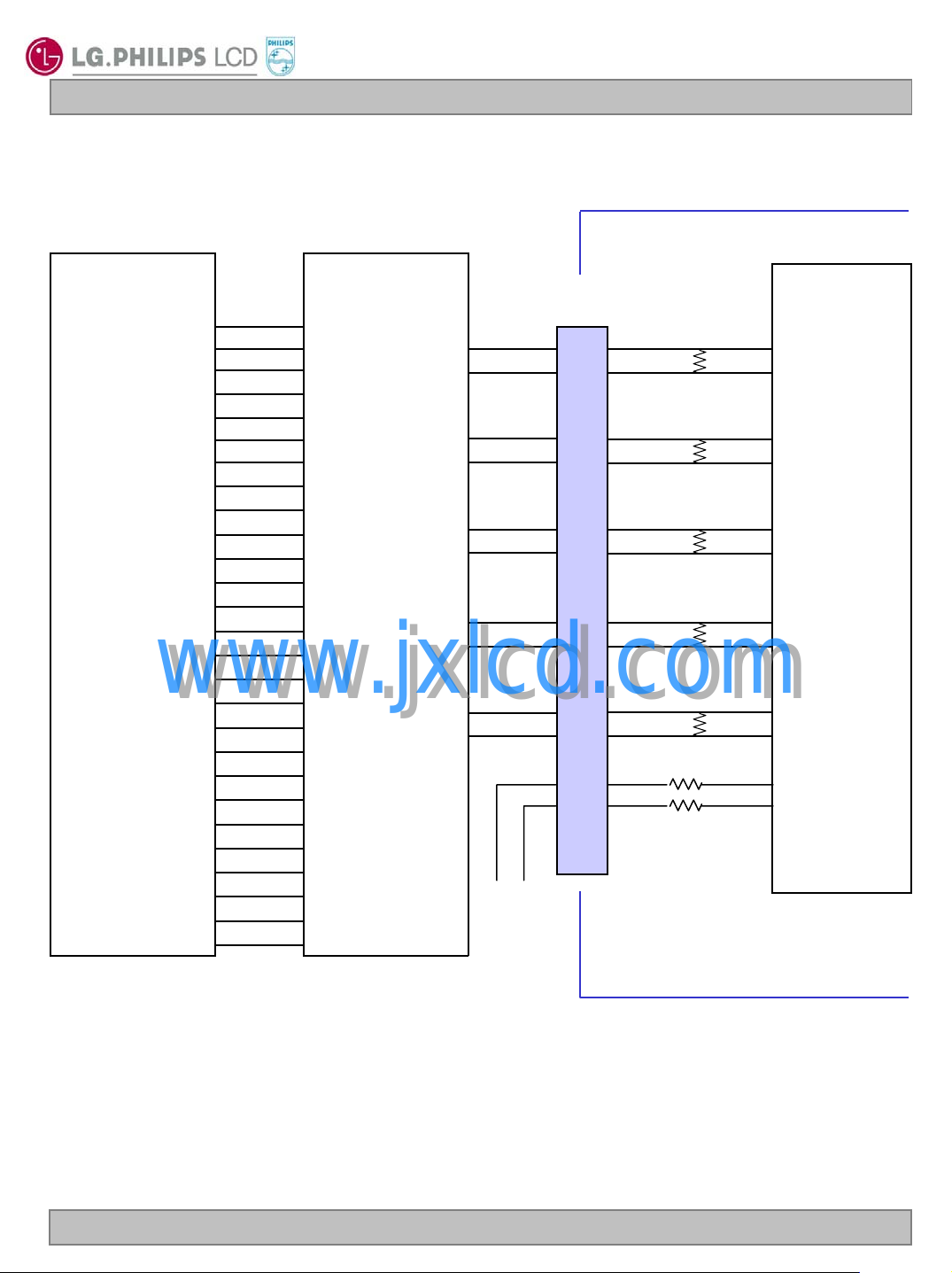
3-2. Interface Connections
This LCD employs two kinds of interface connection, a 30-pin connector is used for the module electronics and t wo 12pin Connectors are used for the integral backlight system.
3-2-1. LCD Module
- LCD Connector(CN1) : FI-X30SSL-HF (Manufactured by JAE)
- Mating Connector : FI-X30C2L (Manufactured by JAE)
Table 3. MODULE CONNECTOR(CN1) PIN CONFIGURATION
Pin No. Symbol Description Note
1
2
3
4
5
6
7
8
9
10
11
12
13
14
15
16
17
18
www.jxlcd.com
19
20
21
22
23
24
25
26
27
28
29
30
www.jxlcd.com
Note: 1. If the pin no. 9 is Ground, Interface format is “LG”, and if the pin no. 9 is Vcc(3.3V), Interface format
is “DISM”. See page 9 and 10.
2. The pin no. 30 is necessary for LCD test.
When LVDS signals are abnormal operation more than 3-Vsync times and power 12V is supplied,
‘Open’ or ‘Vcc’ : LCD operate itself some test patterns.(AGP – Auto Generation Pattern)
‘Ground’ : LCD operate itself a black pattern. (NSB – No Signal Black)
LPL recommend ‘Ground’ for NSB.
3. All GND (ground) pins should be connected together, which should be also connected to the LCD
module’s metal frame.
4. All V
LCD (power input) pins should be connected together.
5. Input Levels of LVDS signals are based on the IEA 664 Standard.
6. If the pin no. 28 is ‘Open’ or ‘Vcc’, Pol period is “1 Frame” and if the pin is Ground,
Pol period is “2 Frame with gamma swing”.
Ver. 0.0 Jan.17, 2006
VLCD Power Supply +12.0V
VLCD Power Supply +12.0V
VLCD Power Supply +12.0V
VLCD Power Supply +12.0V
GND Ground
GND Ground
GND Ground
GND Ground
Select Select LVDS Data format
NC NC
GND Ground
RA- LVDS Receiver Signal(-)
RA+ LVDS Receiver Signal(+)
GND Ground
RB- LVDS Receiver Signal(-)
RB+ LVDS Receiver Signal(+)
GND Ground
RC- LVDS Receiver Signal(-)
RC+ LVDS Receiver Signal(+)
GND Ground
RCLK- LVDS Receiver Clock Signal(-)
RCLK+ LVDS Receiver Clock Signal(+)
GND Ground
RD- LVDS Receiver Signal(-)
RD+ LVDS Receiver Signal(+)
GND Ground
NC NC
Select Select Inversion mode
GND Ground
NC(GND) LCD test
1
6
2
8/ 28
LC200WX1
Liquid Crystal Display
Product Specification
Table 4. REQUIRED SIGNAL ASSIGNMENT FOR LVDS TRANSMITTER ( Pin9=“L” or “Open” )
Host System
24 Bit
RED0
RED1
RED2
RED3
RED4
RED5
RED6
RED7
GREEN0
GREEN1
GREEN2
GREEN3
GREEN4
GREEN5
GREEN6
GREEN7
www.jxlcd.com
BLUE0
www.jxlcd.com
BLUE1
BLUE2
BLUE3
BLUE4
BLUE5
BLUE6
BLUE7
Hsync
Vsync
Data Enable
CLOCK
DS90C385
or Compatible
51
52
54
55
56
3
50
2
4
6
7
11
12
14
8
10
15
19
20
22
23
24
16
18
27
28
30
31
TxOUT0TxOUT0+
TxOUT1TxOUT1+
TxOUT2TxOUT2+
TxCLKOUTTxCLKOUT+
TxOUT3TxOUT3+
FI-X30SSL-HF
48
47
46
45
42
41
40
39
38
37
GND
GND
12
13
15
16
18
19
21
22
24
25
30
Timing
Controller
100Ω
100Ω
100Ω
100Ω
100Ω
9
RxIN0RxIN0+
RxIN1RxIN1+
RxIN2RxIN2+
RxCLKINRxCLKIN+
RxIN3RxIN3+
LG / DISM
LCD Test
LCD Module
Note: 1. The LCD Module uses a 100 Ohm[Ω] resistor between positive and negative lines of each receiver
input.
2. Refer to LVDS Transmitter Data Sheet for detail descriptions. (DS90C385 or Compatible)
3. ‘7’ means MSB and ‘0’ means LSB at R,G,B pixel data.
Ver. 0.0 Jan.17, 2006
9/ 28

Product Specification
Table 5. REQUIRED SIGNAL ASSIGNMENT FOR LVDS TRANSMITTER ( Pin9=“H” )
LC200WX1
Liquid Crystal Display
Host System
24 Bit
RED0
RED1
RED2
RED3
RED4
RED5
RED6
RED7
GREEN0
GREEN1
GREEN2
GREEN3
GREEN4
GREEN5
GREEN6
GREEN7
www.jxlcd.com
BLUE0
www.jxlcd.com
BLUE1
BLUE2
BLUE3
BLUE4
BLUE5
BLUE6
BLUE7
Hsync
Vsync
Data Enable
CLOCK
DS90C385
or Compatible
50
2
51
52
54
55
56
3
8
10
4
6
7
11
12
14
16
18
15
19
20
22
23
24
27
28
30
31
TxOUT0TxOUT0+
TxOUT1TxOUT1+
TxOUT2TxOUT2+
TxCLKOUTTxCLKOUT+
TxOUT3TxOUT3+
FI-X30SSL-HF
48
47
46
45
42
41
40
39
38
37
GND
Vcc
12
13
15
16
18
19
21
22
24
25
30
Timing
Controller
100Ω
100Ω
100Ω
100Ω
100Ω
9
RxIN0RxIN0+
RxIN1RxIN1+
RxIN2RxIN2+
RxCLKINRxCLKIN+
RxIN3RxIN3+
LG /
DISM
LCD Test
LCD Module
Note: 1. The LCD Module uses a 100 Ohm[Ω] resistor between positive and negative lines of each receiver
input.
2. Refer to LVDS Transmitter Data Sheet for detail descriptions. (DS90C385 or Compatible)
3. ‘7’ means MSB and ‘0’ means LSB at R,G,B pixel data.
Ver. 0.0 Jan.17, 2006
10 / 28

Product Specification
3-2-2. Backlight Inverter
- Inverter Connector : S14B-PH-SM3 Side entry type (manufactured by JST)
- Mating Connector : PHR-14 or Equivalent
Table 6. INVERTER CONNECTOR PIN CONFIGULATION
Pin Symbol Signal assignment Note
1VBL 24V Power Input
LC200WX1
Liquid Crystal Display
2V
3V
4
524V Power Input
6
7
8
9
10
11 VBR-A Analog dimming 0V(min) ~ 3.3V(max)
12 ON / OFF Backlight ON/OFF control
www.jxlcd.com
www.jxlcd.com
BL 24V Power Input
BL 24V Power Input
BL
V
VBL
GND
GND
GND
GND
GND
BR
-B
EXTV
Error out
24V Power Input
GROUND
GROUND
GROUND
GROUND
GROUND
External PWM signal13
Backlight status output14
1
ON : 2.4 ~ 5.0V
OFF : 0.0 ~ 0.8V
Rising edge : Lamp on
Falling edge : Lamp off
Normal : 0V
Abnormal : External pull-up
Note :
1. GND is connected to the LCD module’s metal frame.
PCB
1 2
(JST : Japan Solderless Terminal Co.,Ltd.)
Ver. 0.0 Jan.17, 2006
3
JST S14B-PH-SM3
12
13
14
11 / 28

LC200WX1
Liquid Crystal Display
Product Specification
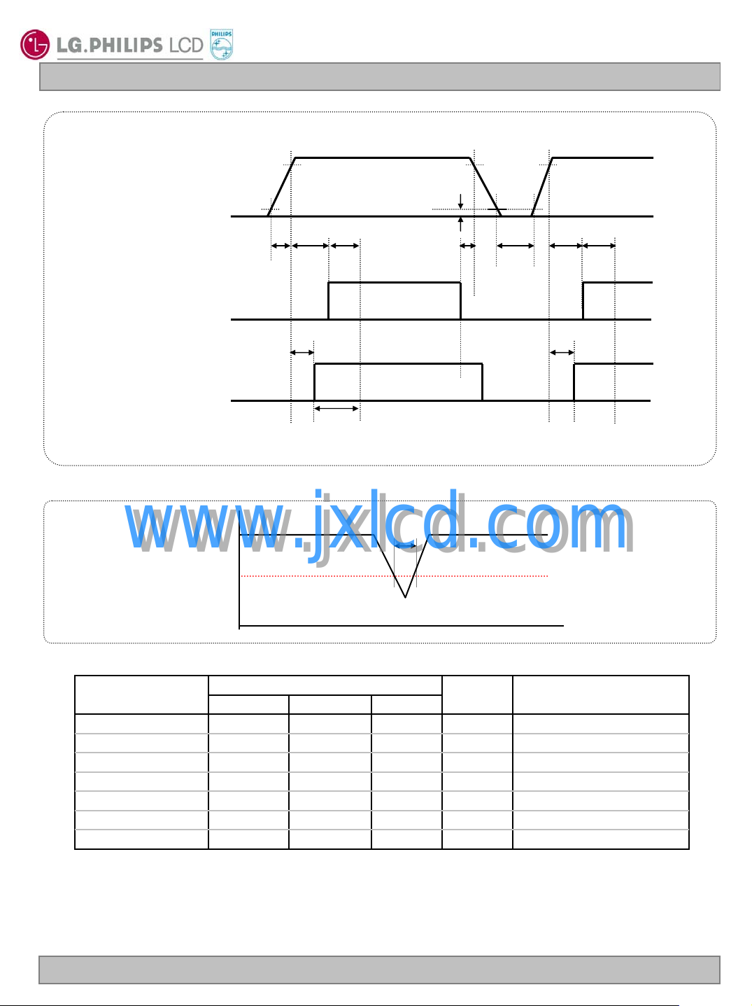
3-3. Signal Timing Specifications
This is the signal timing required at the input of LVDS Transmitter. All of the interface signal timing should be
satisfied with the following specifications for it’s proper operation.
Table 7. TIMMING TABLE
ITEM Symbol Min. Typ. Max.
Clock
Hsync
Vsync
Notes:
1. The performance of the electro-optical characteristics are may be influenced by
variance of the vertical refresh rates.
2. Above timing table is only valid for DE Mode.
3. H sync, V sync don’t care.(for only DE Mode.)
Period t
Frequency f
Frequency
Display Valid
Blank
Total t
Frequency f
Display Valid t
Blank t
Total t
www.jxlcd.com
www.jxlcd.com
CLK
CLK
f
H
t
HV
t
HT-tHV
HT
V
VV
VT-tVV
VT
12.2
68 72.3 82 MHz
45
1366
90
1456 1528 1776 Clks
47
768
7
775 790 1063 Lines
13.8 14.7
47.4
1366
162
60
768
22
53
1366
410
66
768
295
Unit Note
ns
KHZ
Clks
Clks
HZ
Lines
Lines
PAL :
47~53Hz,
NTSC :
57~66Hz
Ver. 0.0 Jan.17, 2006
12 / 28

3-4. Signal Timing Waveforms
LC200WX1
Liquid Crystal Display
Product Specification
DCLK
1366
DE(Data Enable)
tCLK
DE(Data Enable)
www.jxlcd.com
www.jxlcd.com
0.5 Vcc
Invalid data
DE, Data
tHT
Valid data
1
0.7VDD
tHV
0.3VDD
1366
Invalid data
768
Ver. 0.0 Jan.17, 2006
1 768
tVT
tVV
13 / 28

LC200WX1
Liquid Crystal Display
Product Specification
3-5. Color Data Reference
The brightness of each primary color(red,green,blue) is based on the 8-bit gray scale data input for the color
the higher the binary input, the brighter the co lor. The table below pro vides a reference fo r colo r ver sus data
input.
Table 8. COLOR DATA REFERENCE
Input Color Data
Basic
Color
RED
Color
Black 0 0 0 0 0 0 0 0 0 0 0 0 0 0 0 0 0 0 0 0 0 0 0 0
Red (255)
Green (255)
Blue (255)
Cyan
Magenta
Yellow
White
www.jxlcd.com
www.jxlcd.com
RED (000) Dark 0 0 0 0 0 0 0 0 0 0 0 0 0 0 0 0 0 0 0 0 0 0 0 0
RED (001) 0 0 0 0 0 0 0 1 0 0 0 0 0 0 0 0 0 0 0 0 0 0 0 0
... ... ... ...
RED (254) 1 1 1 1 1 1 1 0 0 0 0 0 0 0 0 0 0 0 0 0 0 0 0 0
RED (255) 1 1 1 1 1 1 1 1 0 0 0 0 0 0 0 0 0 0 0 0 0 0 0 0
GREEN (000) Dark 0 0 0 0 0 0 0 0 0 0 0 0 0 0 0 0 0 0 0 0 0 0 0 0
MSB LSB
R7 R6 R5 R4 R3 R2 R1 R0 G7 G6 G5 G4 G3 G2 G1 G0 B7 B6 B5 B4 B3 B2 B1 B0
1 1 1 1 1 1 1 1 0 0 0 0 0 0 0 0 0 0 0 0 0 0 0 0
0 0 0 0 0 0 0 0 1 1 1 1 1 1 1 1 0 0 0 0 0 0 0 0
0 0 0 0 0 0 0 0 0 0 0 0 0 0 0 0 1 1 1 1 1 1 1 1
0 0 0 0 0 0 0 0 1 1 1 1 1 1 1 1 1 1 1 1 1 1 1 1
1 1 1 1 1 1 1 1 0 0 0 0 0 0 0 0 1 1 1 1 1 1 1 1
1 1 1 1 1 1 1 1 1 1 1 1 1 1 1 1 0 0 0 0 0 0 0 0
1 1 1 1 1 1 1 1 1 1 1 1 1 1 1 1 1 1 1 1 1 1 1 1
RED
MSB LSB
GREEN
BLUE
MSB LSB
GREEN (001) 0 0 0 0 0 0 0 0 0 0 0 0 0 0 0 1 0 0 0 0 0 0 0 0
GREEN
GREEN (254) 0 0 0 0 0 0 0 0 1 1 1 1 1 1 1 0 0 0 0 0 0 0 0 0
GREEN (255) 0 0 0 0 0 0 0 0 1 1 1 1 1 1 1 1 0 0 0 0 0 0 0 0
BLUE (000) Dark
BLUE (001) 0 0 0 0 0 0 0 0 0 0 0 0 0 0 0 0 0 0 0 0 0 0 0 1
BLUE
BLUE (254) 0 0 0 0 0 0 0 0 0 0 0 0 0 0 0 0 1 1 1 1 1 1 1 0
BLUE (255) 0 0 0 0 0 0 0 0 0 0 0 0 0 0 0 0 1 1 1 1 1 1 1 1
Ver. 0.0 Jan.17, 2006
... ... ... ...
0 0 0 0 0 0 0 0 0 0 0 0 0 0 0 0 0 0 0 0 0 0 0 0
... ... ... ...
14 / 28

3-6. Power Sequence
3-6-1. Sequence for LCD Module
Power Supply For LCD
V
LCD
0V
Product Specification
90% 90%
10%
T
1 T2 T5 T6 T7
LC200WX1
Liquid Crystal Display
10%
Interface Signal
(Tx & Option )
Power for Lamp
Table 9. POWER SEQUENCE
www.jxlcd.com
www.jxlcd.com
Parameter
T1 0.01 - 20 ms
T2 0.01 - 50 ms
T3 200 - - ms
T5 0.01 - 50 ms
T6 - - - ms
T7 2.0 - - s
10% 10%
Min Typ Max
Valid Data
T3 T4
Lamp ON
Value
Unit
msT4 200 - -
Note : 1. Please avoid floating state of interface signal at invalid period.
2. When the interface signal is invalid, be sure to pull down the power supply V
3. The case when the T2/T5 exceed maximum specification, it operates protection
pattern(Black pattern) till valid signal inputted. There is no reliability problem.
4. The T3/T4 is recommended value, the case when failed to meet a minimum specification,
abnormal display would be shown. There is no reliability problem.
Ver. 0.0 Jan.17, 2006
LCD
to 0V.
15 / 28
3-6-2. Sequence for Inverter
LC200WX1
Liquid Crystal Display
Product Specification
Power Supply For Inverter
90%
V BL
10%
0V
T1 T2
V ON/OFF
Vbr-A
ExtVbr-B : 1. Lamp ON at PWM Rising Edge and Lamp OFF at PWM Falling Edge.
2. EXTVBR-B has Same sequence with Vbr-A
3-6-3. Deep condition for Inverter
www.jxlcd.com
www.jxlcd.com
24V (typ.)
0.7V
1000ms (Min) 1000ms (Min)
T4
Lamp ON
T7
T6
T5
T3 T2
V
T4
BL
: 24V
V
(Typ.) x 0.85
BL
Table 11. Power Sequence for Inverter
Parameter
T1 20 - - ms 1
T2 500 - - ms
T3 200 - - ms
T4 0 T5 10 - - ms
T6 - - 10 ms V
T7 1000 - - ms
Note : 1. T1 describes rising time of 0V to 24V and is not applied at restarting time.
2. When the Inverter is shut-down by ARC protection, T3 need 3.3sec
3. When V
4. T4(max) is less than T2.
5. In T7 section, ExtVbr-B should be duty 100% and Vbr-A is recommended 3.3V.
Ver. 0.0 Jan.17, 2006
BL
Min Typ Max
(24V) is supplied always, there is no reliability problem.
Values
Units
ms 4, 5
0 V
Remarks
2
(Typ) x 0.85
BL
16 / 28
LC200WX1
Liquid Crystal Display
Product Specification
4. Optical Specification
Optical characteristics are determined after the unit has been ‘ON’ for 30min in a dark environment at 25±2°C.
The values specified are at an approximate distance 50cm from the LCD surface at a viewing angle of Φ and
θ equal to 0 °.
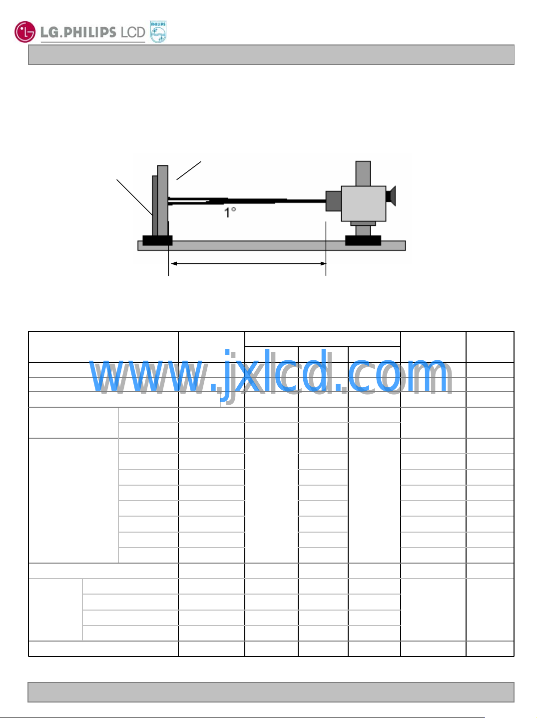
It is presented additional information concerning the measurement equipment and method in FIG. 1.
Optical Stage(x,y)
FIG. 1 Optical Characteristic Measurement Equipment and Method
Table 11. OPTICAL CHARACTERISTICS
Parameter Symbol
Contrast Ratio CR 400 600
Surface Luminance, white L
Luminance Variation δ
Response Time
Color Coordinates
[CIE1931]
Viewing Angle (CR>10)
Gray Scale 6
www.jxlcd.com
www.jxlcd.com
Rise Time Tr
Decay Time
RED
GREEN
BLUE
WHITE
x axis, right(φ=0°) θr 85 89 -
x axis, left (φ=180°)
y axis, up (φ=90°)
y axis, down (φ=270°)
LCD Module
WH
WHITE
5P 1.3 3
R
Tr
D
Rx 0.636
Ry 0.342
Gx 0.280
Gy 0.605
Bx 0.146
By 0.064
Wx 0.276
Wy 0.280
θl 85 89 -
θu 85 89 -
θd 85 89 -
50cm
Ta= 25±2°C, V
Min Typ Max
330 430 cd/m
- 8 16
- 9 16
Typ
-0.03
=12.0V, fV=60Hz, Dclk=72MHz, Vbr-A =3.3V,
LCD
Value
Pritchard 880 or
equivalent
ExtVbr=100%
Unit Note
2
ms 4
Typ
+0.03
degree 5
1
2
Ver. 0.0 Jan.17, 2006
17 / 28
Product Specification
Notes 1. Contrast Ratio(CR) is defined mathematically as :
Surface Luminance with all white pixels
Contrast Ratio =
Surface Luminance with all black pixels
It is measured at the center point(1).
2. Surface luminance is luminance value at the center point across the LCD surface 50cm from the
surface with all pixels displaying white.
For more information, see FIG 2.
3. The variation in surface lumin ance , δ WHITE is defined as :
, L
δ WHITE(5P) = Maximum(L
Where L
For more information, see FIG 2.
on1
to L
are the luminance with all pixels displaying white at 5 locations .
on5
on1,Lon2
, ...... , L
on3
) / Minimum(L
on5
on1,Lon2
LC200WX1
Liquid Crystal Display
, L
, ..... , L
on3
on5
)
4. Response time is the time required for the display to transition from black to white (Rise Time, Tr
and from white to black (Decay Time, Tr
For additional information, see FIG 3.
5. Viewing angle is the angle at which the contrast ratio is greater than 10. The angles are
determined for the horizontal or x axis and the vertical or y axis with respect to the z axis which
is normal to the LCD surface. For more information, see FIG 4.
6. Gray scale specification
Gamma Value is approximately 2.2.
For more information, see Table 12.
Table 12. GRAY SCALE SPECIFICATION
www.jxlcd.com
www.jxlcd.com
Gray Level Luminance [%] (Typ)
L0
L15
L31
L47
L63
L79
L95
L111
L127
L143
L159
L175
L191
L207
L223
L239
L255
).
D
0.16
0.34
1.13
2.71
5.20
9.06
13.9
19.3
25.0
32.0
40.1
48.9
58.2
68.5
79.1
89.3
100
)
R
Ver. 0.0 Jan.17, 2006
18 / 28
Product Specification
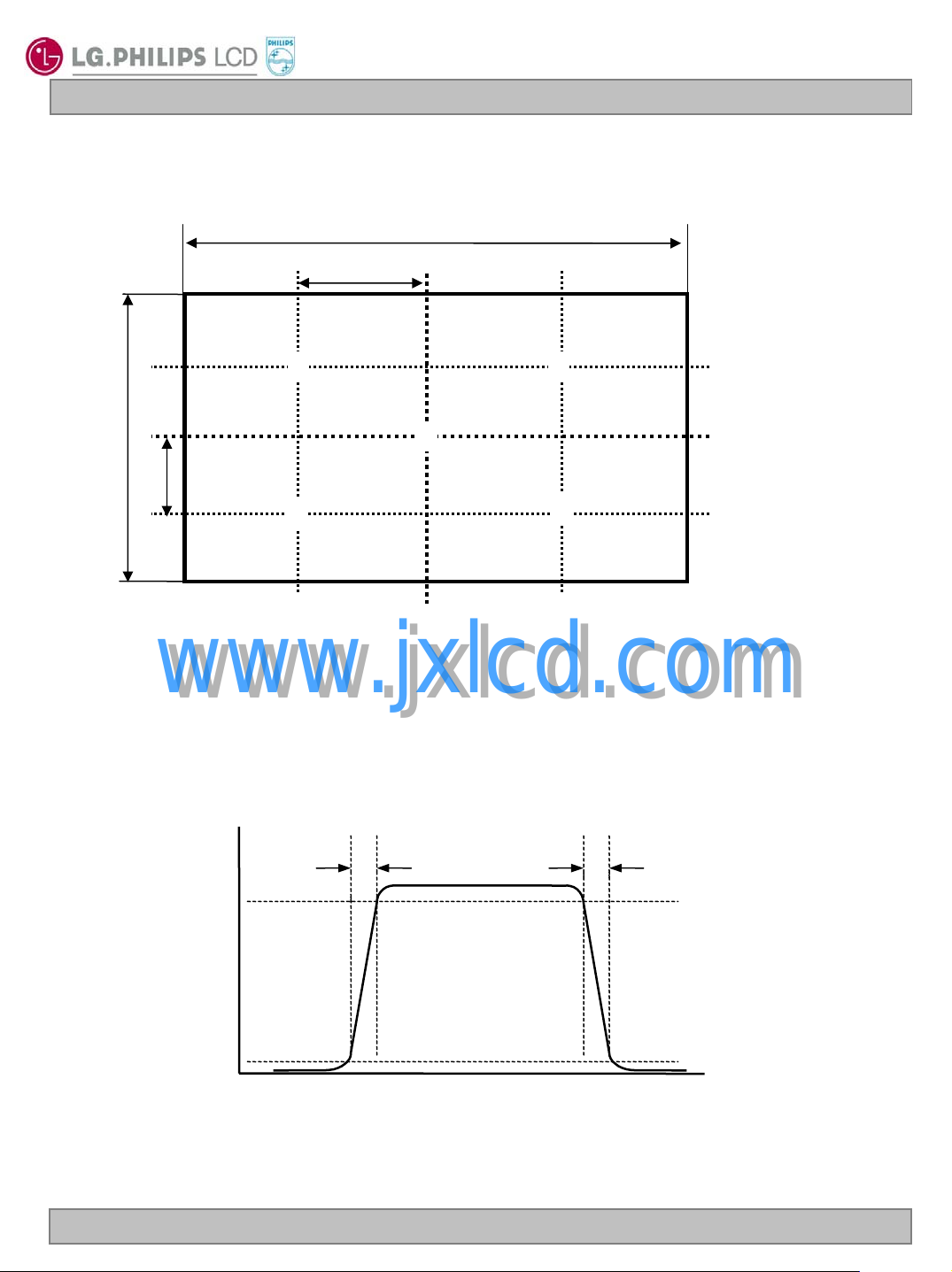
Measuring point for surface luminance & measuring point for luminance variation
H
A
③②
LC200WX1
Liquid Crystal Display
V
B
④
FIG. 2 Measure Point for Luminance
www.jxlcd.com
www.jxlcd.com
The response time is defined as the following figure and shall be measured by switching the input signal for
Black to White and White to Black.
%
100
90
TrR
①
⑤
A : H / 4 mm
B : V / 4 mm
H : 443.609mm
V : 249.408mm
@ H,V : Active Area
TrD
Optical
Response
10
0
FIG. 3 Response Time
Ver. 0.0 Jan.17, 2006
WhiteBlack
Black
19 / 28

LC200WX1
Liquid Crystal Display
Product Specification
Dimension of viewing angle range
φ
= 180°, Left
φ
= 270°, Down
Optical characteristics are determined after the unit has been ‘ON’ for 30min in a dark environment at 25±2°C.
The values specified are at an approximate distance 1.2mm from the LCD surface at a viewing angle of Φ and θ
equal to 0 °.
It is presented additional information concerning the measurement equipment and method in FIG. 1.
Normal
θ
φ
FIG. 4 Viewing Angle
E
Y
φ
= 90°, Up
φ
= 0°, Right
EZ Contrast
UP
θl=135˚
θr=45˚
www.jxlcd.com
www.jxlcd.com
θu=225˚
FIG. 5 Diagonal Viewing Angle Measurement Condition
7. Image sticking
When it changes into pattern-B after a 1-hour drive by pattern-A, it disappears within 10 minutes.
<Pattern-A, Chess board (8x6)> <Pattern-B, Mid-gray(127 gray)>
1.2 ~ 1.5㎜
θd=315˚
DOWN
θ=0˚
Ver. 0.0 Jan.17, 2006
20 / 28
LC200WX1
Liquid Crystal Display
Product Specification
5. Mechanical Characteristics
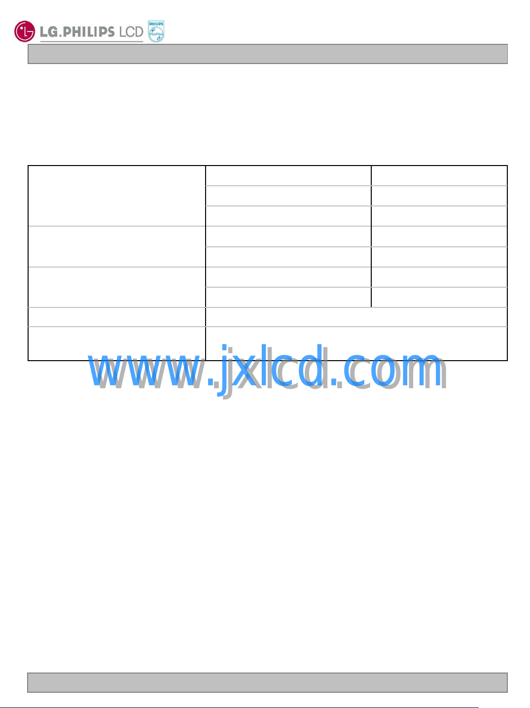
The following items provide general mechanical characteristics. In addition the figures in the next page are
detailed mechanical drawing of the LCD module.
Table 13. MECHANICAL CHARACTE RISTIC S
Horizontal 472.0mm
Outline Dimension
Bezel Area
Active Display Area
Weight (Typ.) 2,800 (g), (Max.) 3,000(g)
Surface Treatment
www.jxlcd.com
Note : Please refer to a mechanic drawing in terms of tolerance at the next page.
www.jxlcd.com
Vertical
Depth 38.0mm
Horizontal 448.0mm
Vertical 253.8mm
Horizontal
Vertical
Hard coating(3H)
Anti-glare treatment of the front polarizer
275.0mm
443.609mm
249.408mm
Ver. 0.0 Jan.17, 2006
21 / 28
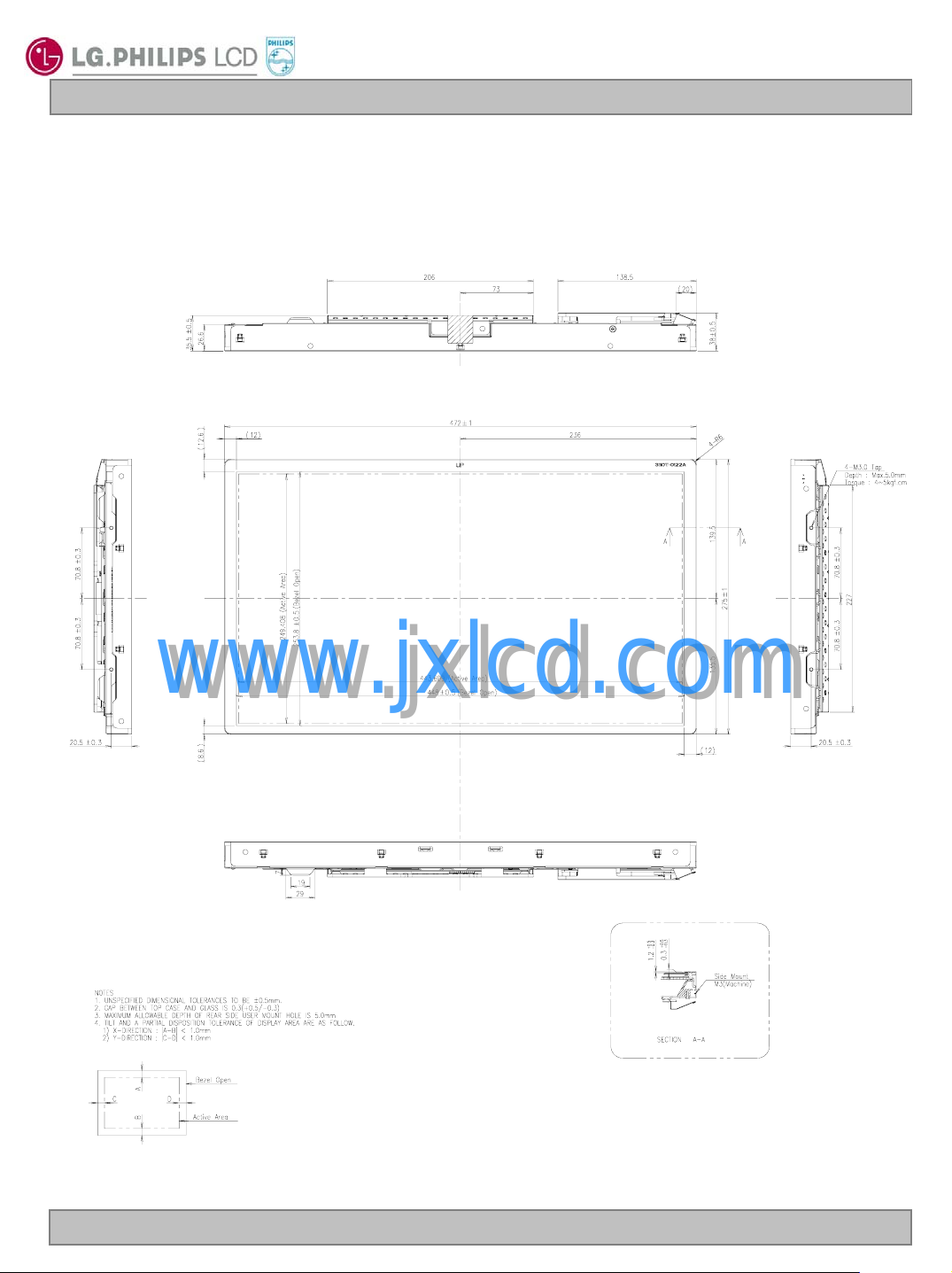
<FRONT VIEW>
LC200WX1
Liquid Crystal Display
Product Specification
www.jxlcd.com
www.jxlcd.com
Ver. 0.0 Jan.17, 2006
22 / 28
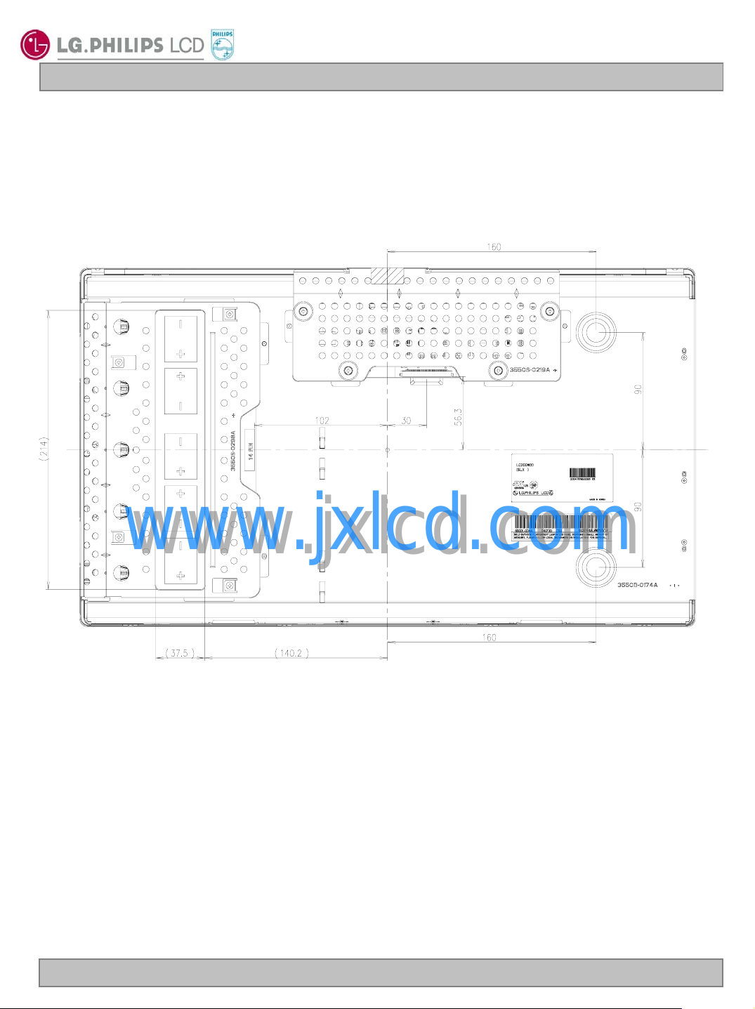
<REAR VIEW>
LC200WX1
Liquid Crystal Display
Product Specification
www.jxlcd.com
www.jxlcd.com
Ver. 0.0 Jan.17, 2006
23 / 28
Product Specification
6. Reliability
Table 14. ENVIRONMENT TEST CONDITION
No. Test Item Condition
1 High temperature storage test Ta= 50°C 240h
2 Low temperature storage test Ta= -20°C 240h
3 High temperature operation test Ta= 40°C 50%RH 240h
4 Low temperature operation test Ta= 0°C 240h
Wave form : random
5
Vibration test
(non-operating)
Vibration level : 1.0G RMS
Bandwidth : 10-500Hz
Duration : X,Y,Z, 10 min
One time each direction
LC200WX1
Liquid Crystal Display
Shock level : 100G
6
7 Humidity condition Operation Ta= 40 °C, 90%RH
8
Shock test
(non-operating)
www.jxlcd.com
www.jxlcd.com
Altitude operating
storage / shipment
Waveform : half sine wave, 2ms
Direction : ±X, ±Y, ±Z
One time each direction
0 - 14,000 feet(4267.2m)
0 - 40,000 feet(12192m)
Ver. 0.0 Jan.17, 2006
24 / 28
LC200WX1
Liquid Crystal Display
Product Specification
7. International standards
7-1. Safety
a) UL 60950, Third Edition, Underwriters Laboratories, Inc., Dated Dec. 11, 2000.
Standard for Safety of Information Technology Equipment, Including Electrical Business Equipment.
b) CAN/CSA C22.2, No. 60950, Third Edition, Canadian Standards Association, Dec. 1, 2000.
Standard for Safety of Information Technology Equipment, Including Electrical Business Equipment.
c) EN 60950 : 2000, Third Edition
IEC 60950 : 1999, Third Edition
European Committee for Electrotechnical Standardization(CENELEC)
EUROPEAN STANDARD for Safety of Information Technology Equipment Including Electrical
Business Equipment.
7-2. EMC
a) ANSI C63.4 “Methods of Measurement of Radio-Noise Emissions from Low-Voltage Electrical and
Electrical Equipment in the Range of 9kHZ to 40GHz. “American National Standards Institute(ANSI),
1992
b) C.I.S.P.R “Limits and Methods of Measurement of Radio Interface Characteristics of Information
Technology Equipment.“ International Special Committee on Radio Interference.
c) EN 55022 “Limits and Methods of Measurement of Radio Interface Characteristics of Information
Technology Equipment.“ European Committee for Electrotechnical Standardization.(CENELEC), 1998
( Including A1: 2000 )
www.jxlcd.com
www.jxlcd.com
Ver. 0.0 Jan.17, 2006
25 / 28

Product Specification
8. Packing
8-1. Designation of Lot Mark
a) Lot Mark
ABCDEFGHI JKLM
A,B,C : SIZE(INCH) D : YEAR
E : MONTH F : FACTORY CODE
G : ASSEMBLY CODE H ~ M : SERIAL NO.
Note
1. YEAR
LC200WX1
Liquid Crystal Display
Year
Mark
2. MONTH
Month
Mark
www.jxlcd.com
www.jxlcd.com
3. FACTORY CODE
Factory Code LPL Gumi LPL Nanjing HEESUNG
Mark C DK
4. SERIAL NO.
Mark
b) Location of Lot Mark
Serial No. is printed on the label. The label is attached to the backside of the LCD module.
This is subject to change without prior notice.
100001~199999, 200001~299999, 300001~399999, …., A00001~A99999, ….., Z00001~Z99999
200320022001
321
200452005
4
Apr5May
4
2006720078200892009
6
Jun7Jul8Aug9Sep
6
2010
0
Oct
A
Nov
B
DecMarFebJan
C321
8-2. Packing Form
a) Package quantity in one box : 4 pcs
b) Box Size : 530mm X 310mm X 327mm
Ver. 0.0 Jan.17, 2006
26 / 28

LC200WX1
Liquid Crystal Display
Product Specification
9. Precautions
Please pay attention to the followings when you use this TFT LCD module.
9-1. Mounting Precautions
(1) You must mount a module using holes arranged in four corners or four sides.
(2) You should consider the mounting structure so that uneven force (ex. Twisted stress) is not applied to the
module. And the case on which a module is mounted should have sufficient strength so that external
force is not transmitted directly to the module.
(3) Please attach the surface transparent protective plate to the surface in order to protect the polarizer.
Transparent protective plate should have sufficient strength in order to the resist external force.
(4) You should adopt radiation structure to satisfy the temperature specification.
(5) Acetic acid type and chlorine type materials for the cover case are not desirab le because the former
generates corrosive gas of attacking the polarizer at high temper ature and the latter causes cir cuit break
by electro-chemical reaction.
(6) Do not touch, push or rub the exposed polarizers with glass, tweezers or anything harder than HB
pencil lead. And please do not rub with dust clothes with chemical treatment.
Do not touch the surface of polarizer for bare hand or greasy cloth.(Some cosmetics are detrimental
to the polarizer.)
(7) When the surface becomes dusty, please wipe gently with absorbent cotton or other soft mater ials like
chamois soaks with petroleum benzine. Normal-hexane is recommended for cleaning the adhesives
used to attach front / rear polarizers. Do not use acetone, toluene and alcohol because they cause
chemical damage to the polarizer.
(8) Wipe off saliva or water drops as soon as possible. Their long time contact with polarizer causes
deformations and color fading.
(9) Do not open the case because inside circuits do not have sufficient strength.
www.jxlcd.com
www.jxlcd.com
9-2. Operating Precautions
(1) The spike noise causes the mis-operation of circuits. It should be lower than following voltage :
V=±200mV(Over and under shoot voltage)
(2) Response time depends on the temperature.(In lower temperature, it becomes longer.)
(3) Brightness depends on the temperature. (In lower temperature, it becomes lower.)
And in lower temperature, response time(required time tha t br ightness is stab le after tu rned on ) beco mes
longer.
(4) Be careful for condensation at sudden temperature change. Condensation makes damage to polarize r or
electrical contacted parts. And after fading condensation, smear or spot will occur.
(5) When fixed patterns are displayed for a long time, remnant image is likely to occur.
(6) Module has high frequency cir cuits. Sufficient suppression to the elec tromagnetic interference shall be
done by system manufacturers. Grounding and shielding methods may be important to minimized the
interference.
(7) Please do not give any mechanical and/or acoustical impact to LCM. O therwise, LCM can’t be operated
its full characteristics perfectly.
(8) A screw which is fastened up the steels should be a machine screw.
(if not, it causes metallic foreign material and deal LCM a fatal blow)
(9) Please do not set LCD on its edge.
Ver. 0.0 Jan.17, 2006
27 / 28

LC200WX1
Liquid Crystal Display
Product Specification
9-3. Electrostatic Discharge Control
Since a module is composed of electronic circuits, it is not strong to elec trosta tic di scharge. Make cer tain that
treatment persons are connected to ground through wrist band etc. And don’t touch interface pin directly.
9-4. Precautions for Strong Light Exposure
Strong light exposure causes degradation of polarizer and color filter.
9-5. Storage
When storing modules as spares for a long time, the following precautions are necessary.
(1) Store them in a dark place. Do not expo se t he mo dul e t o sunli ght or flu orescen t ligh t. Ke e p th e t emp erature
between 5°C and 35°C at normal humidity.
(2) The polarizer surface should not come in contact with any other object.
It is recommended that they be stored in the container in which they were shipped.
9-6. Handling Precautions for Protection Film
(1) The protection film is attached to the bezel with a small masking tape.
When the protection film is peeled off, static electricity is generated between the film and polarizer.
This should be peeled off slowly and care fully by people who are electrically g rounded and with well ionblown equipment or in such a condition, etc.
(2) When the module with protection film a ttached is stored for a long time, sometimes there remains a very
small amount of glue still on the bezel after the protection film is peeled off.
(3) You can remove the glue easily. When the glue remains on the bezel surface o r its vestige is r ecognized,
please wipe them off with absorbent cotton waste or other soft materi al like chamois soaked with normalhexane.
www.jxlcd.com
www.jxlcd.com
Ver. 0.0 Jan.17, 2006
28 / 28
 Loading...