

Page 1
(◆) Preliminary Specification
( ) Final Specification
Title 17” SXGA TFT LCD
LB170E01-SL01
Liquid Crystal Display
Product Specification
SPECIFICATION
FOR
APPROVAL
Customer
MODEL
APPROVED BY
/
/
/
SIGNATURE
SUPPLIER LG Display Co., Ltd.
*MODEL LB170E01
Suffix SL01
*When you obtain standard approval,
please use the above model name without suffix
APPROVED BY
Y. T. Woo / G.Manager
REVIEWED BY
K. H. Choi / Manager [C]
B. C. Lee / Manager [M]
J. K. Kim / Manager [P]
PREPARED BY
B. Y. Ha / Engineer
SIGNATURE
Please return 1 copy for your confirmation with
your signature and comments.
Ver. 0.3 Jun. 18. 2013
Note : This document is preliminary version. The latest version must be checked from LG Display before detail design.
Products Engineering Dept.
LG Display Co., Ltd
1 / 31
Page 2
Product Specification
Contents
LB170E01-SL01
Liquid Crystal Display
No ITEM
COVER
CONTENTS
RECORD OF REVISIONS
1 GENERAL DESCRIPTION
2 ABSOLUTE MAXIMUM RATINGS
3 ELECTRICAL SPECIFICATIONS
3-1 ELECTRICAL CHARACTREISTICS
3-2 INTERFACE CONNECTIONS
3-3 SIGNAL TIMING SPECIFICATIONS
3-4 SIGNAL TIMING WAVEFORMS
3-5 COLOR INPUT DATA REFERNECE
3-6 POWER SEQUENCE
3-7 V
4 OPTICAL SFECIFICATIONS
Power Dip Condition
LCD
Page
1
2
3
4
5
6
6
8
13
14
15
16
17
18
5 MECHANICAL CHARACTERISTICS
6 RELIABLITY
7 INTERNATIONAL STANDARDS
7-1 SAFETY
7-2 EMC
7-3 ENVIRONMENT
8 PACKING
8-1 DESIGNATION OF LOT MARK
8-2 PACKING FORM
9 PRECAUTIONS 30
Ver. 0.3 Jun. 18. 2013
Note : This document is preliminary version. The latest version must be checked from LG Display before detail design.
24
27
28
28
28
28
29
30
29
2 / 31
Page 3
Product Specification
RECORD OF REVISIONS
LB170E01-SL01
Liquid Crystal Display
Revision
No
0.0 Mar. 13. 2013 - First Draft, Preliminary Specifications
0.1 May. 01. 2013 4 Change General Features
0.2 Jun. 10. 2013 4 Change General Features
0.3 Jun. 18. 2013 10 Change Flat Link (THINE:THC63LVD823) Transmitter
Revision
Date
Page Description
6 Change Electrical Characteristics
9 Change Mating Connector
24 Change Weight
5 Change ABSOLUTE MAXIMUM RATINGS
6 Change LCD Module ELECTRICAL CHARACTERISTICS
13 Change Timing Table
18 Change OPTICAL CHARACTERISTICS
27 Change Reliability
Ver. 0.3 Jun. 18. 2013
Note : This document is preliminary version. The latest version must be checked from LG Display before detail design.
3 / 31
Page 4
LB170E01-SL01
Liquid Crystal Display
Product Specification
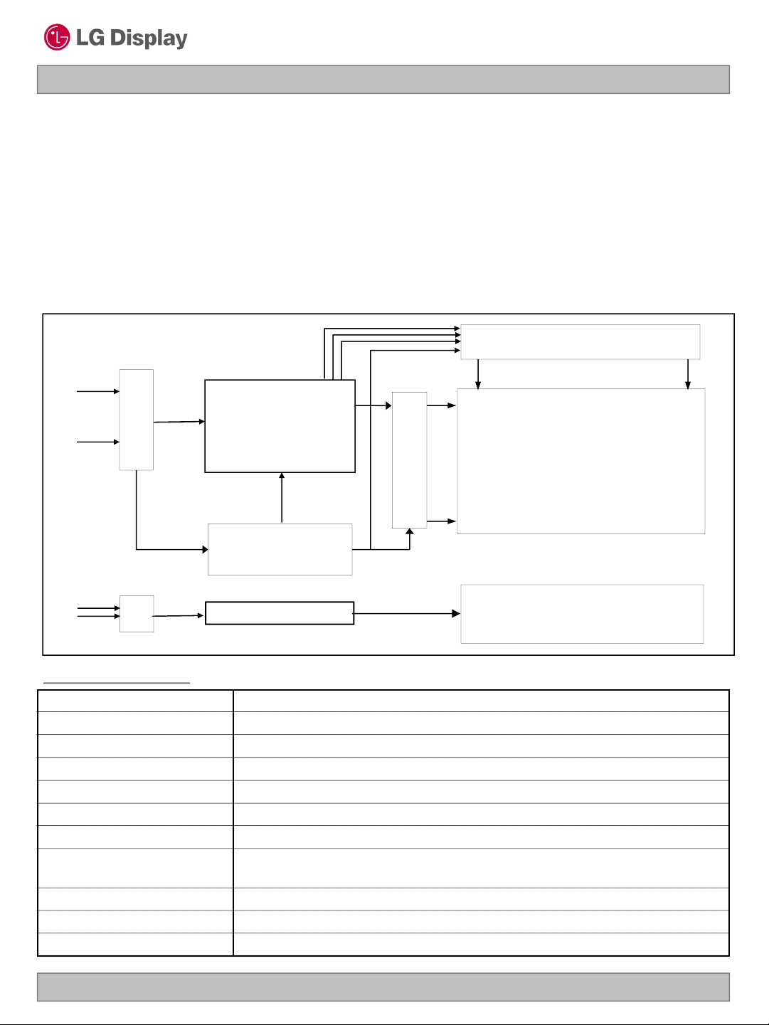
1. General Description
LB170E01 is a Color Active Matrix Liquid Crystal Display with an integral Light Emitting Diode (White LED)
backlight system. The matrix employs a-Si Thin Film Transistor as the active element.
It is a transmissive type display operating in the normally black mode. It has a 17.0 inch diagonally
measured active display area with SXGA resolution (1024 vertical by 1280 horizontal pixel array)
Each pixel is divided into Red, Green and Blue sub-pixels or dots which are arranged in vertical stripes.
Gray scale or the brightness of the sub-pixel color is determined with a 8-bit gray scale signal for each dot,
thus, presenting a palette of more than 16,7M colors
It has been designed to apply the 8Bit 2 port LVDS interface.
It is intended to support displays where high brightness, super wide viewing angle,
high color saturation, and high color are important.
EPI (RGB)
RGB
Source Driver Circuit
LVDS
2port
+5.0V
CN1
(30pin)
Timing
Controller
G1
Gate Driver Circuit
S1 S1280
TFT - LCD Panel
(1280 × RGB × 1024 pixels)
G1024
+5.0V
Power Circuit Block
+12.0V
On/Off,
PWM
General Features
CN2
(6pin)
LED Driver
[ Figure 1 ] Block diagram
Back light Assembly
(LED)
Active Screen Size 17.0 inch (432.75mm) diagonal
Outline Dimension 368.0(H) x 306.0(V) x 14.3(D) mm(Typ.)
Pixel Pitch 0.264 mm x 0.264mm
Pixel Format 1280 horiz. by 1024 vert. Pixels. RGB stripe arrangement
Color Depth 16,7M colors
Luminance, White 400 cd/m
2
( Center 1 Point, Typ.)
Viewing Angle(CR>10) View Angle Free (R/L 178(Typ.), U/D 178(Typ.))
Power Consumption Total 14.75 Watt (Typ.) (2.75 Watt @VLCD, 12 Watt @VBL)
Weight 1260 g (typ.)
Display Operating Mode Transmissive mode, normally black
Surface Treatment Hard coating(3H), Anti-Glare treatment of the front polarizer
Ver. 0.3 Jun. 18. 2013
Note : This document is preliminary version. The latest version must be checked from LG Display before detail design.
4 / 31
Page 5
LB170E01-SL01
Liquid Crystal Display
Product Specification
2. Absolute Maximum Ratings
The following are maximum values which, if exceeded, may cause faulty operation or damage to the unit.
Table 1. ABSOLUTE MAXIMUM RATINGS
Parameter Symbol
Power Input Voltage
Operating Temperature
Storage Temperature
Operating Ambient Humidity
Storage Humidity
VLCD -0.3 6.0 Vdc at 25 2°C
TOP -10 70
TST -20 80
HOP 10 90 %RH
HST 10 90 %RH
Values
Units Notes
Min Max
°C
°C
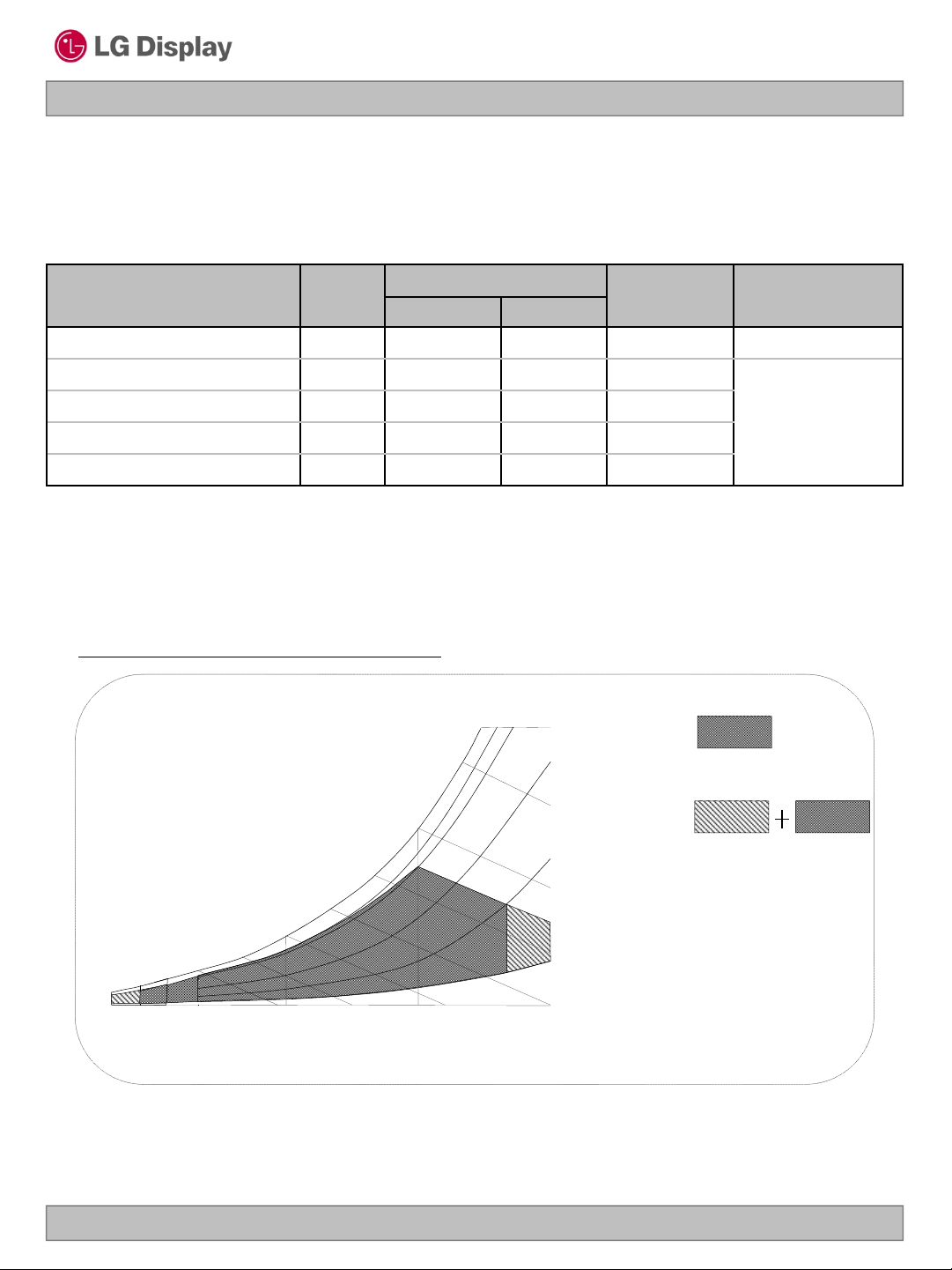
Note : 1. Temperature and relative humidity range are shown in the figure below.
Wet bulb temperature should be 39 °C Max, and no condensation of water.
2. Maximum Storage Humidity is up to 40℃, 70% RH only for 4 corner light leakage Mura.
3. Storage condition is guaranteed under packing condition
FIG.2 Temperature and relative humidity
80%
90%
60
60%
1, 2, 3
[ Operation ]
30%
10%
Humidity[(%)RH]
[ Storage ]
-30
-20
Wet Bulb
Temperature [℃]
10
0
-10
10
50
40
30
20
20 30 40 50
60 700
80
Dry Bulb Temperature [℃]
Ver. 0.3 Jun. 18. 2013
Note : This document is preliminary version. The latest version must be checked from LG Display before detail design.
5 / 31
Page 6
LB170E01-SL01
Liquid Crystal Display
Product Specification
3. Electrical Specifications
3-1. Electrical Characteristics
It requires two power inputs. One is employed to power the LCD electronics and to drive the TFT array and
liquid crystal. The second input power for the LED/Backlight, is typically generated by a LED Driver.
The LED Driver is an internal unit to the LCDs.
Table 2-1. LCD Module ELECTRICAL CHARACTERISTICS
Parameter Symbol
MODULE :
Power Supply Input Voltage VLCD
Power Supply Input Current ILCD
Pc TYP -
Power Consumption
Pc MAX -
Differential Impedance Zm 90 100 110 Ohm
Rush current IRUSH - - 3.0 A 3
BACKLIGHT(With LED Driver):
LED Power Supply Voltage VBL 11.5 12 12.5 V
LED Power Supply Current IBL - 1000 1300 mA
LED Power Consumption PBL - 12 15.6 Watt
PWM Duty Ratio 10 100 %
PWM Dimming Frequency FPWM TBD KHz
PWM Duty High Voltage VH 3.0 3.3 3.6 Vdc
Min Typ Max
4.5 5.0 5.5
-
-
Values
550 715
800 1040
2.75 3.58
4.0 5.2
Unit Notes
Vdc
mA 1
mA 2
Watt 1
Watt 2
PWM Duty Low Voltage VL 0.0 0.3 Vdc
Backlight Enable Voltage VON - 3.3 - Vdc
Backlight Disable Voltage VOFF - 0 - Vdc
Life Time LED_LT 50,000 - - Hrs 7
Ver. 0.3 Jun. 18. 2013
Note : This document is preliminary version. The latest version must be checked from LG Display before detail design.
6 / 31
Page 7
LB170E01-SL01
Liquid Crystal Display
Note :
1. The specified current and power consumption are under the V
Product Specification
=5.0V, 25 °C,fV=60Hz condition
LCD
whereas Typical Power Pattern[Mosaic] shown in the [ Figure 3 ] is displayed.
2. The current is specified at the maximum current pattern.
3. Maximum Condition of Inrush current :
The duration of rush current is about 5ms and rising time of power Input is 500us 20%.(min.).
4. The current and power consumption with LED Driver are under the VBL = 12.0V, 25°C, Dimming of
Max luminance and White pattern with the normal frame frequency operated(60Hz).
5. The operation of LED Driver below minimum dimming ratio may cause flickering or reliability issue.
6. This Spec. is not effective at 100% dimming ratio as an exception because it has DC level equivalent
to 0Hz. In spite of acceptable range as defined, the PWM Frequency should be fixed and stable for
more consistent brightness control at any specific level desired.
7. The life is determined as the time at which luminance of the LED is 50% compared to that of initial
value at the typical LED current on condition of continuous operating at 25 2°C
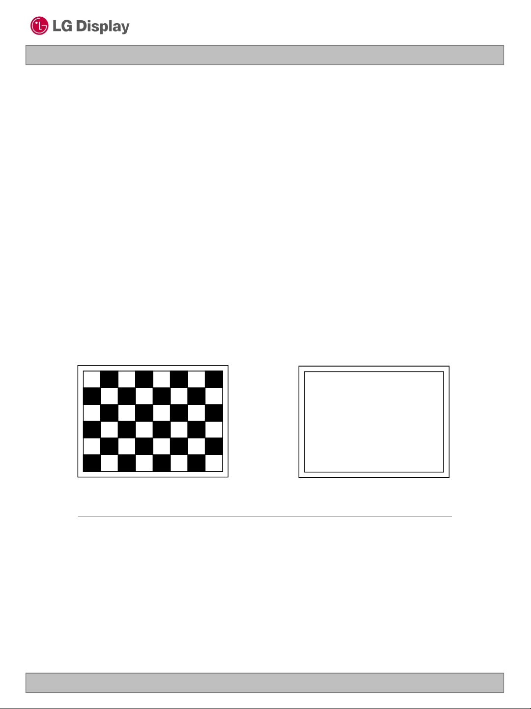
Typical power Pattern
Maximum power Pattern
FIG.3 Mosaic pattern & White Pattern for power consumption measurement
Ver. 0.3 Jun. 18. 2013
Note : This document is preliminary version. The latest version must be checked from LG Display before detail design.
7 / 31
Page 8
LB170E01-SL01
Liquid Crystal Display
Product Specification
3-2. Interface Connections
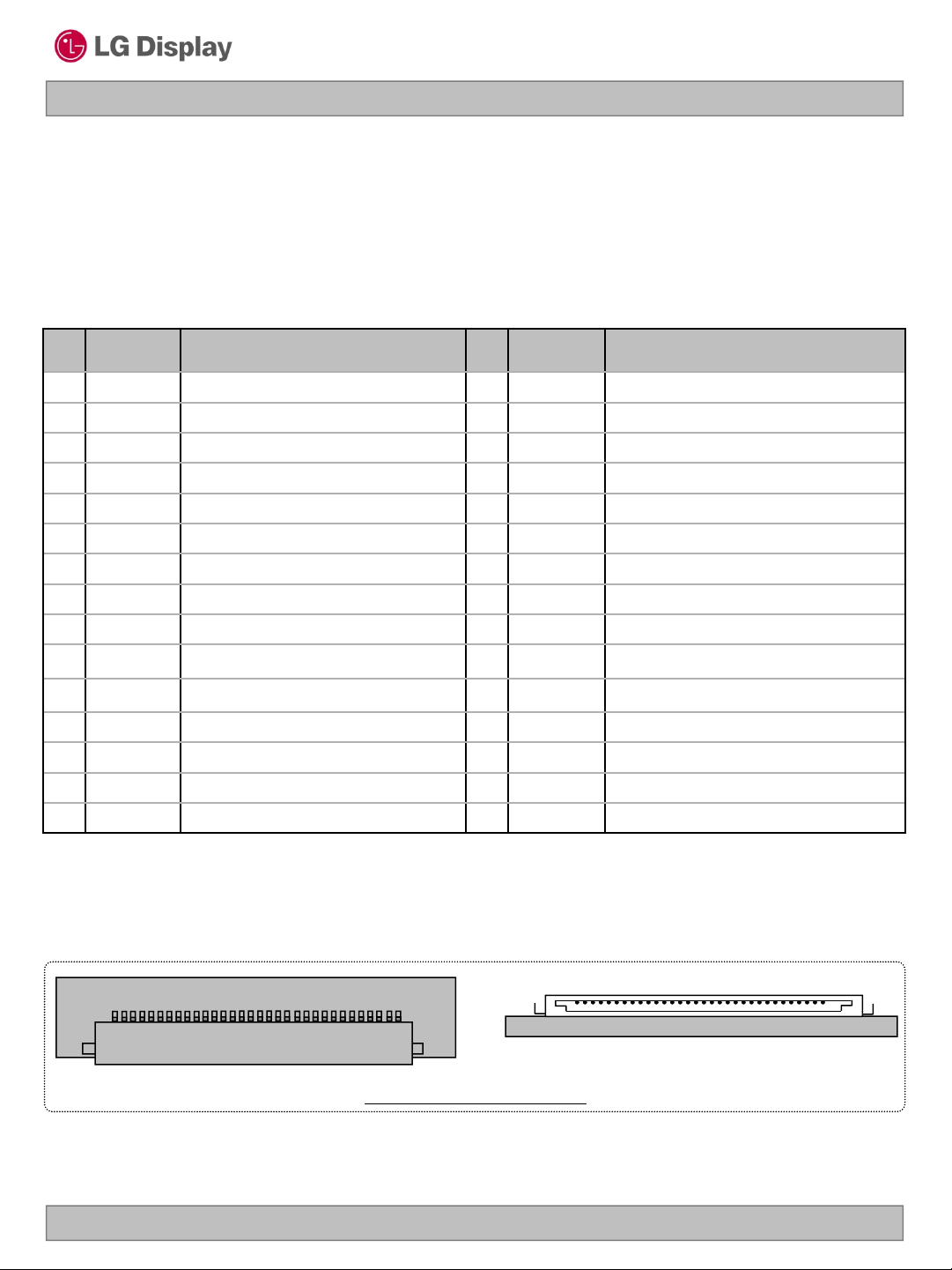
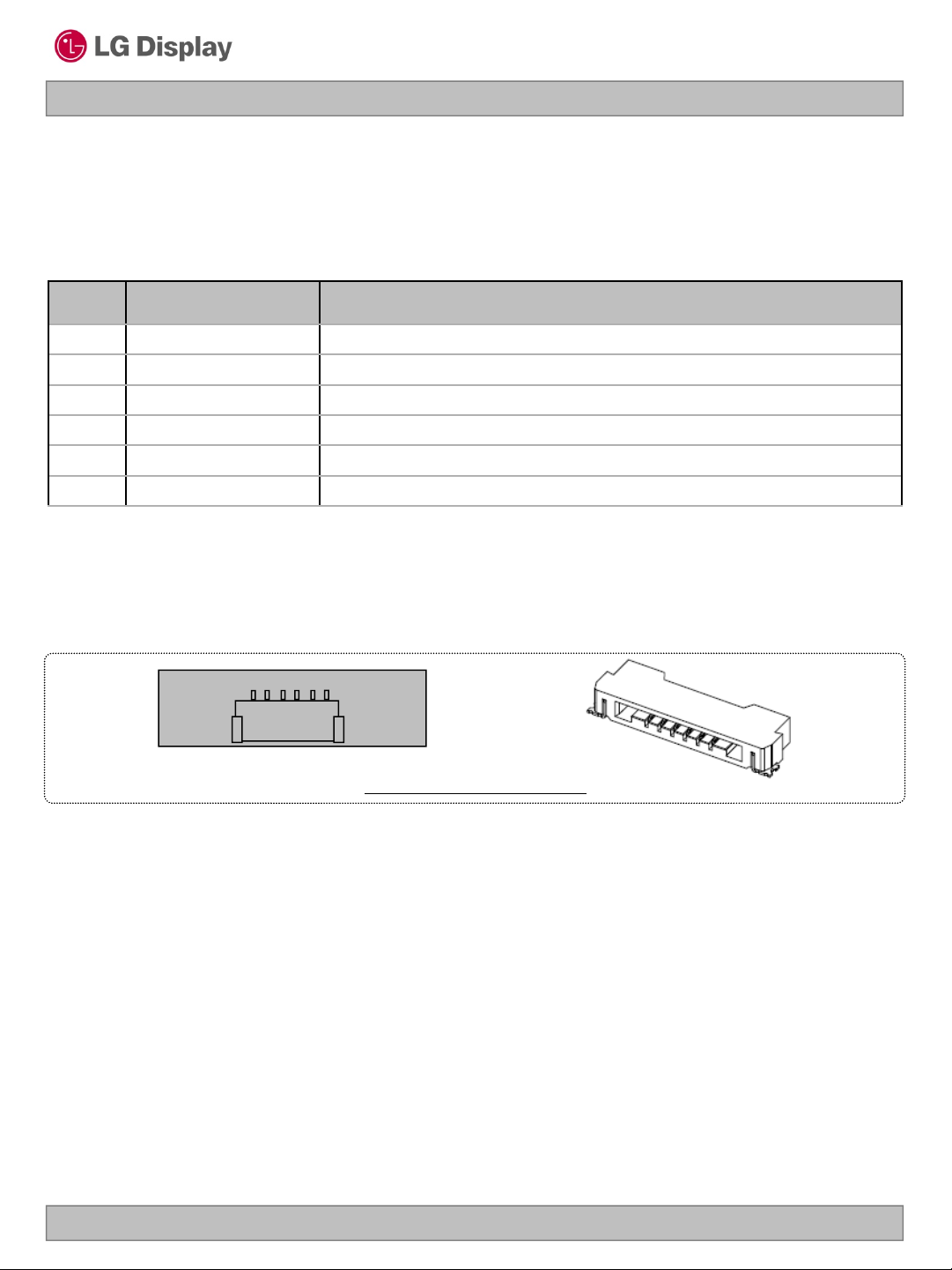
3-2-1. LCD Module
- LCD Connector(CN1). : GT101-30S-H16 (LGC) , IN-30-BA10 (UJU)
- Mating Connector : FI-X30C2L (Manufactured by JAE) or Equivalent
Table 3. MODULE CONNECTOR(CN1) PIN CONFIGURATION
No Symbol Description No Symbol Symbol
1
2
3
4
5
6
7
8
9
10
11
12
13
14
15
FR0M
FR0P
FR1M
FR1P
FR2M
FR2P
GND
FCLKINM
FCLKINP
FR3M
FR3P
SR0M
SR0P
GND
SR1M
Minus signal of odd channel 0 (LVDS)
Plus signal of odd channel 0 (LVDS)
Minus signal of odd channel 1 (LVDS)
Plus signal of odd channel 1 (LVDS)
Minus signal of odd channel 2 (LVDS)
Plus signal of odd channel 2 (LVDS)
Ground
Minus signal of odd clock channel (LVDS)
Plus signal of odd clock channel (LVDS)
Minus signal of odd channel 3 (LVDS)
Plus signal of odd channel 3 (LVDS)
Minus signal of even channel 0 (LVDS)
Plus signal of even channel 0 (LVDS)
Ground
Minus signal of even channel 1 (LVDS)
16
17
18
19
20
21
22
23
24
25
26
27
28
29
30
SR1P
GND
SR2M
SR2P
SCLKINM
SCLKINP
SR3M
SR3P
GND
NC
NC
NC
VLCD
VLCD
VLCD
Plus signal of even channel 1 (LVDS)
Ground
Minus signal of even channel 2 (LVDS)
Plus signal of even channel 2 (LVDS)
Minus signal of even clock channel (LVDS)
Plus signal of even clock channel (LVDS)
Minus signal of even channel 3 (LVDS)
Plus signal of even channel 3 (LVDS)
Ground
No Connection.(I2C Serial interface for LCM)
No Connection.(I2C Serial interface for LCM)
No Connection.
Power Supply +5.0V
Power Supply +5.0V
Power Supply +5.0V
Note: 1. All GND(ground) pins should be connected together and to Vss which should also be connected to
the LCD’s metal frame.
2. All VLCD (power input) pins should be connected together.
3. Input Level of LVDS signal is based on the IEA 664 Standard.
#1 #30
GT101-30S-H16(LGC) or
IN-30-BA 10 (UJU)
FIG.4 Connector diagram
Ver. 0.3 Jun. 18. 2013
Note : This document is preliminary version. The latest version must be checked from LG Display before detail design.
#1 #30
Rear view of LCM
8 / 31
Page 9
Product Specification
3-2-2. BACKLIGHT
- BACKLIGHT Connector(CN2). : IS100-L06B-C20 (UJU)
- Mating Connector : HS100-L06N-N20 (Manufactured by UJU) or Equivalent
Table 4. BACKLIGHT CONNECTOR(CN2) PIN CONFIGURATION
No Symbol Description
LB170E01-SL01
Liquid Crystal Display
1
VBL
2
VBL
3
VBL
4
GND
5
On/Off
6
PWM
Backlight Power Supply(12.0 Typ.)
Backlight Power Supply(12.0 Typ.)
Backlight Power Supply(12.0 Typ.)
Ground
Backlight On/Off, High(3.3V Typ.): On, Low(Ground): Off
PWM Dimming Signal
Note: 1. All GND(ground) pins should be connected together and the LCD’s metal frame.
2. All VBL (power input) pins should be connected together.
#1
IS100-L06B-C20(UJU)
#6
FIG.5 Connector diagram
Ver. 0.3 Jun. 18. 2013
Note : This document is preliminary version. The latest version must be checked from LG Display before detail design.
9 / 31
Page 10
LB170E01-SL01
Liquid Crystal Display
Product Specification
Table 4. REQUIRED SIGNAL ASSIGNMENT FOR Flat Link (THINE:THC63LVD823) Transmitter
Pin# Pin Name Descrption Pin# Pin Name Descrption
1 B24 The 2nd Pixel Data Input 51 R10 The 1st Pixel Data Input
2 B25 The 2nd Pixel Data Input 52 R11 The 1st Pixel Data Input
3 VCC Power Supply for TTL input 53 R12 The 1st Pixel Data Input
4 GND Ground for TTL input 54 R13 The 1st Pixel Data Input
5 B26 The 2nd Pixel Data Input 55 VCC Power Supply for TTL input
6 B27 The 2nd Pixel Data Input 56 GND Ground for TTL input
7 HSYNC Hsync Input 57 R14 The 1st Pixel Data Input
8 VSYNC Vsync Input 58 R15 The 1st Pixel Data Input
9 DE Data Enable Input 59 R16 The 1st Pixel Data Input
10 CLKIN Clock Input 60 R17 The 1st Pixel Data Input
11 R/F Input Clock Triggering Edge Select 61 G10 The 1st Pixel Data Input
12 RS LVDS swig range select 62 G11 The 1st Pixel Data Input
13 TEST1 Test pin 63 G12 The 1st Pixel Data Input
14 TEST2 Test pin 64 G13 The 1st Pixel Data Input
15 MODE1 Pixel Data Mode 65 G14 The 1st Pixel Data Input
16 MODE0 Pixel Data Mode 66 G15 The 1st Pixel Data Input
17 OE Output enable 67 G16 The 1st Pixel Data Input
18 6/8 6bit/8bit color select 68 G17 The 1st Pixel Data Input
19 /PDWN Power down 69 B10 The 1st Pixel Data Input
20 TEST3 Test pin 70 B11 The 1st Pixel Data Input
21 TEST4 Test pin 71 VCC Power Supply for TTL input
22 TEST5 Test pin 72 GND Ground for TTL input
23 PLL GND Ground for PLL circuitry 73 B12 The 1st Pixel Data Input
24 PLL VCC Power Supply for PLL circuitry 74 B13 The 1st Pixel Data Input
25 PLL GND Ground for PLL circuitry 75 B14 The 1st Pixel Data Input
26 LVDS GND Ground for LVDS output 76 B15 The 1st Pixel Data Input
27 TD2+ The 2nd Link. The 2nd pixel output data 77 B16 The 1st Pixel Data Input
28 TD2- The 2nd Link. The 2nd pixel output data 78 B17 The 1st Pixel Data Input
29 TCLK2+ LVDS Clock Out for 2nd Link 79 B20 The 2nd Pixel Data Input
30 TCLK2- LVDS Clock Out for 2nd Link 80 B21 The 2nd Pixel Data Input
31 TC2 The 2nd Link. The 2nd pixel output data 81 B22 The 2nd Pixel Data Input
32 TC2+ The 2nd Link. The 2nd pixel output data 82 B23 The 2nd Pixel Data Input
33 LVDS VCC Power Supply for LVDS Output 83 B24 The 2nd Pixel Data Input
34 TB2+ The 2nd Link. The 2nd pixel output data 84 B25 The 2nd Pixel Data Input
35 TB2- The 2nd Link. The 2nd pixel output data 85 B26 The 2nd Pixel Data Input
36 TA2+ The 2nd Link. The 2nd pixel output data 86 B27 The 2nd Pixel Data Input
37 TA2- The 2nd Link. The 2nd pixel output data 87 VCC Power Supply for TTL input
38 LVDS GND Ground for LVDS output 88 GND Ground for TTL input
39 TD1+ The 1st Link. The 1st Pixel output data 89 G20 The 2nd Pixel Data Input
40 TD1- The 1st Link. The 1st Pixel output data 90 G21 The 2nd Pixel Data Input
41 TCLK1+ LVDS Clock Out for 1st Link 91 G22 The 2nd Pixel Data Input
42 TCLK1- LVDS Clock Out for 1st Link 92 G23 The 2nd Pixel Data Input
43 TC1+ The 1st Link. The 1st Pixel output data 93 G24 The 2nd Pixel Data Input
44 TC1- The 1st Link. The 1st Pixel output data 94 G25 The 2nd Pixel Data Input
45 LVDS VCC Power Supply for LVDS Output 95 G26 The 2nd Pixel Data Input
46 TB1+ The 1st Link. The 1st Pixel output data 96 G27 The 2nd Pixel Data Input
47 TB1- The 1st Link. The 1st Pixel output data 97 B20 The 2nd Pixel Data Input
48 TA1+ The 1st Link. The 1st Pixel output data 98 B21 The 2nd Pixel Data Input
49 TA1- The 1st Link. The 1st Pixel output data 99 B22 The 2nd Pixel Data Input
50 LVDS GND Ground for LVDS output 100 B23 The 2nd Pixel Data Input
Note : Refer to LVDS Transmitter Data Sheet for detail descriptions.
Ver. 0.3 Jun. 18. 2013
10 / 31
Note : This document is preliminary version. The latest version must be checked from LG Display before detail design.
Page 11

LVDS Input characteristics
1. DC Specification
LB170E01-SL01
Liquid Crystal Display
Product Specification
Description Symbol Min Max Unit Notes
LVDS Differential Voltage |VID| 200 600 mV -
LVDS Common mode Voltage V
LVDS Input Voltage Range V
CM
IN
1.0 1.5 V -
0.7 1.8 V -
Change in common mode Voltage ΔVCM - 250 mV -
2. AC Specification
Tclk
LVDS Clock
LVDS Data
Description Symbol Min Max Unit Notes
LVDS Clock to Data Skew Margin
SKEW (Fclk
t
SKEW
t
1) 95 MHz > Fclk ≥85 MHz : - 300 ~ +300
2) 85 MHz > Fclk ≥65 MHz : - 400 ~ +400
3) 65 MHz > Fclk ≥30 MHz : - 600 ~ +600
t
SKEW
t
SKEW
t
SKEW
= 1/T
clk
)
- 300 + 300 ps 95MHz > Fclk ≥ 85MHz
- 400 + 400 ps 85MHz > Fclk ≥ 65MHz
- 600 + 600 ps 65MHz > Fclk ≥ 30MHz
LVDS Clock to Clock Skew Margin
(Even to Odd)
Ver. 0.3 Jun. 18. 2013
t
SKEW_EO
- 1/7 + 1/7 T
clk
-
11 / 31
Note : This document is preliminary version. The latest version must be checked from LG Display before detail design.
Page 12

3. Data Format
1) LVDS 2 Port
LB170E01-SL01
Liquid Crystal Display
Product Specification
< Clock skew margin between channel >
< LVDS Data Format >
Ver. 0.3 Jun. 18. 2013
Note : This document is preliminary version. The latest version must be checked from LG Display before detail design.
12 / 31
Page 13

LB170E01-SL01
Liquid Crystal Display
Product Specification
3-3. Signal Timing Specifications
This is signal timing required at the input of the TMDS transmitter. All of the interface signal timing should be
satisfied with the following specifications for it’s proper operation.
Table 6. TIMING TABLE
ITEM Symbol Min Typ Max Unit Note
DCLK
Horizontal
Vertical
Period tCLK
Frequency -
total tHP
Frequency fH
Blanking
valid tWH
total tVP
Frequency fV
Blanking
valid tWV
14.7 18.5 22.2
45.0 54.0 68.4
672 844 1022
53.3 64.0 82.1
32 204 382
640 640 640
1034 1066 1320
47 60 76
10 42 296
1024 1024 1024
ns
MHz
tCLK
KHz
tCLK
tCLK
tHP
Hz
tHP
tHP
Note:
1. DE Only mode operation. The input of Hsync & Vsync signal does not
have an effect on LCD normal operation.
2. The performance of the electro-optical characteristics may be influenced by variance of the
vertical refresh rates.
3. Horizontal period should be even.
Ver. 0.3 Jun. 18. 2013
Note : This document is preliminary version. The latest version must be checked from LG Display before detail design.
13 / 31
Page 14

3-4. Signal Timing Waveforms
1. DCLK , DE, DATA waveforms
LB170E01-SL01
Liquid Crystal Display
Product Specification
DCLK
tCLK
First data
Second data
DE(Data Enable)
2. Horizontal waveform
Invalid data
Invalid data
Valid data
Pixel 0,0
Valid data
Pixel 1,0
Pixel 2,0
Pixel 3,0
tHV
Invalid data
Invalid data
tHP
DE(Data Enable)
DE
3. Vertical waveform
t
VP
tVV
tHP
DE(Data Enable)
Ver. 0.3 Jun. 18. 2013
Note : This document is preliminary version. The latest version must be checked from LG Display before detail design.
DE
14 / 31
Page 15

LB170E01-SL01
Liquid Crystal Display
Product Specification
3-5. Color Input Data Reference
The Brightness of each primary color(red,green,blue) is based on the 8-bit gray scale data input for the color;
the higher the binary input, the brighter the color. The table below provides a reference for color versus data
input.
Table 7. COLOR DATA REFERENCE
Input Color Data
Basic
Color
RED
Color
Black 0 0 0 0 0 0 0 0 0 0 0 0 0 0 0 0 0 0 0 0 0 0 0 0
Red (255) 1 1 1 1 1 1 1 1 0 0 0 0 0 0 0 0 0 0 0 0 0 0 0 0
Green (255) 0 0 0 0 0 0 0 0 1 1 1 1 1 1 1 1 0 0 0 0 0 0 0 0
Blue (255) 0 0 0 0 0 0 0 0 0 0 0 0 0 0 0 0 1 1 1 1 1 1 1 1
Cyan 0 0 0 0 0 0 0 0 1 1 1 1 1 1 1 1 1 1 1 1 1 1 1 1
Magenta 1 1 1 1 1 1 1 1 0 0 0 0 0 0 0 0 1 1 1 1 1 1 1 1
Yellow 1 1 1 1 1 1 1 1 1 1 1 1 1 1 1 1 0 0 0 0 0 0 0 0
White 1 1 1 1 1 1 1 1 1 1 1 1 1 1 1 1 1 1 1 1 1 1 1 1
RED (000) Dark 0 0 0 0 0 0 0 0 0 0 0 0 0 0 0 0 0 0 0 0 0 0 0 0
RED (001) 0 0 0 0 0 0 0 1 0 0 0 0 0 0 0 0 0 0 0 0 0 0 0 0
... ... ... ...
RED (254) 1 1 1 1 1 1 1 0 0 0 0 0 0 0 0 0 0 0 0 0 0 0 0 0
RED (255) 1 1 1 1 1 1 1 1 0 0 0 0 0 0 0 0 0 0 0 0 0 0 0 0
GREEN (000) Dark 0 0 0 0 0 0 0 0 0 0 0 0 0 0 0 0 0 0 0 0 0 0 0 0
MSB LSB
R7 R6 R5 R4 R3 R2 R1 R0 G7 G6 G5 G4 G3 G2 G1 G0 B7 B6 B5 B4 B3 B2 B1 B0
RED
MSB LSB
GREEN
BLUE
MSB LSB
GREEN (001) 0 0 0 0 0 0 0 0 0 0 0 0 0 0 0 1 0 0 0 0 0 0 0 0
GREEN
GREEN (254) 0 0 0 0 0 0 0 0 1 1 1 1 1 1 1 0 0 0 0 0 0 0 0 0
GREEN (255) 0 0 0 0 0 0 0 0 1 1 1 1 1 1 1 1 0 0 0 0 0 0 0 0
BLUE (000) Dark 0 0 0 0 0 0 0 0 0 0 0 0 0 0 0 0 0 0 0 0 0 0 0 0
BLUE (001) 0 0 0 0 0 0 0 0 0 0 0 0 0 0 0 0 0 0 0 0 0 0 0 1
BLUE
BLUE (254) 0 0 0 0 0 0 0 0 0 0 0 0 0 0 0 0 1 1 1 1 1 1 1 0
BLUE (255) 0 0 0 0 0 0 0 0 0 0 0 0 0 0 0 0 1 1 1 1 1 1 1 1
Ver. 0.3 Jun. 18. 2013
... ... ... ...
... ... ... ...
15 / 31
Note : This document is preliminary version. The latest version must be checked from LG Display before detail design.
Page 16
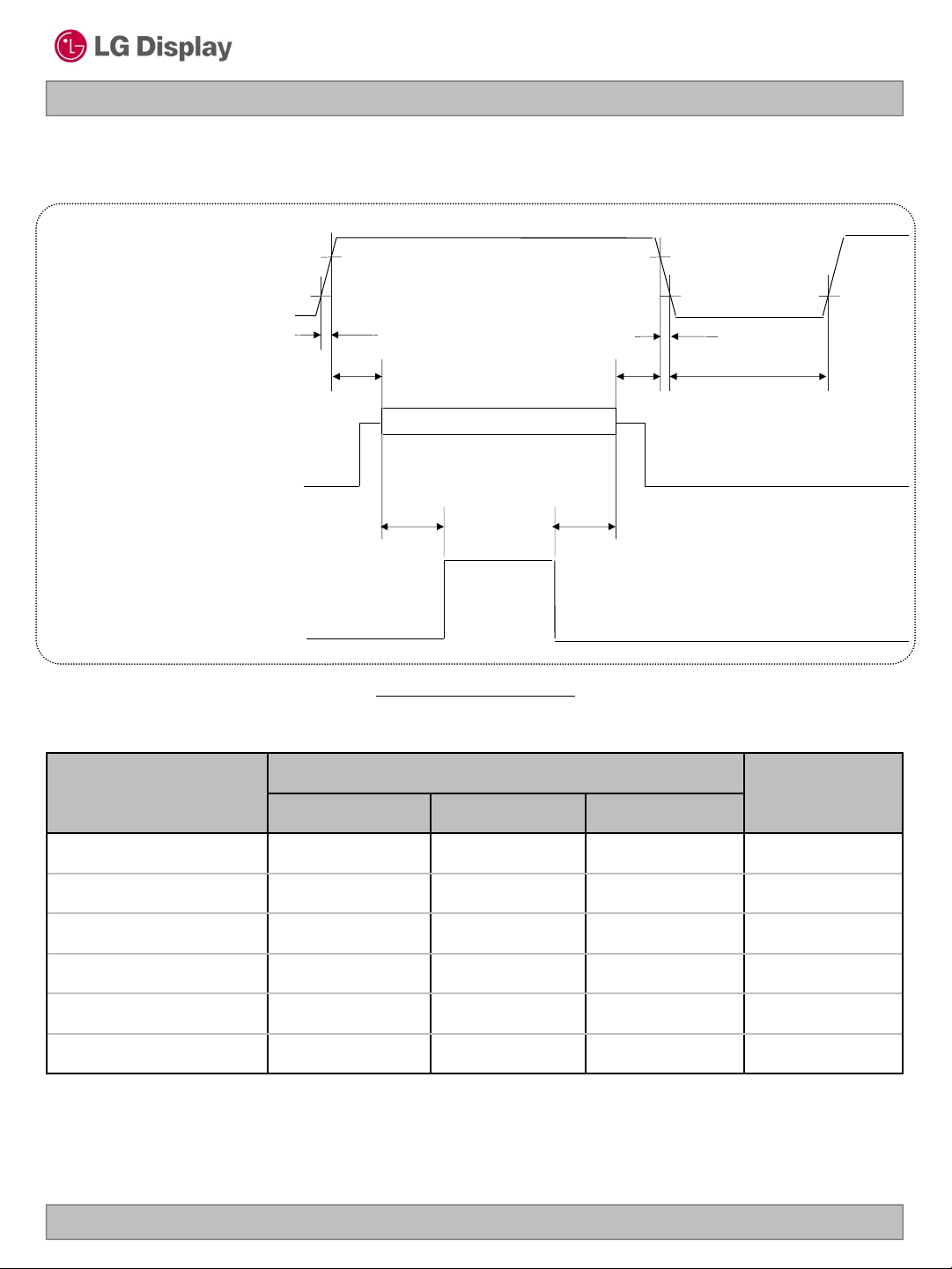
3-6. Power Sequence
Power Supply, VLCD
Interface Signal, Vi
(Digital RGB signal,
SCDT ,Vsync, Hsync,
DE, Clock to PanelLink
Transmitter)
LB170E01-SL01
Liquid Crystal Display
Product Specification
V
0V
LCD
0V
90%
10%
T1
T2 T5 T7
Valid Data
T3
T4
90%
10%
T6
Power Supply for
LED ONLED OFF
Backlight Inverter
FIG.5 Power sequence
Table 8. POWER SEQUENCE
Values
Parameter
Min Typ Max
T1 0.5 - 10 ms
T2 0.01 - 50 ms
T3 500 - - ms
T4 200 - - ms
T5 0.01 - 50 ms
T7 1000 - ms
Notes : 1. Please avoid floating state of interface signal at invalid period.
2. When the interface signal is invalid, be sure to pull down the power supply for LCD V
3. LED power must be turn on after power supply for LCD and interface signal are valid.
LED OFF
Units
LCD
to 0V.
Ver. 0.3 Jun. 18. 2013
Note : This document is preliminary version. The latest version must be checked from LG Display before detail design.
16 / 31
Page 17

Product Specification
LB170E01-SL01
Liquid Crystal Display
3-7. V
LCD
1) Dip condition
Power Dip Condition
t
d
FIG.6 Power dip condition
V
LCD
4.5V
3.5V
2) V
3.5V ≤V
< 3.5V
LCD
V
-dip conditions should also follow the Power On/Off conditions for supply voltage.
LCD
< 4.5V , td≤20ms
LCD
Ver. 0.3 Jun. 18. 2013
Note : This document is preliminary version. The latest version must be checked from LG Display before detail design.
17 / 31
Page 18

LB170E01-SL01
Liquid Crystal Display
Product Specification
4. Optical Specifications
Optical characteristics are determined after the unit has been ‘ON’ for approximately 15 minutes
in a dark environment at 25±2°C. The values specified are at an approximate distance 50cm from the LCD
surface at a viewing angle of and equal to 0 ° and aperture 1 degree.
FIG. 1 presents additional information concerning the measurement equipment and method.
PR 880 or RD 80S
or PR650
Optical Stage(x,y)
LCD Module
50cm
FIG.7 Optical Characteristic Measurement Equipment and Method
Table 9. OPTICAL CHARACTERISTICS
Parameter Symbol
Contrast Ratio CR 600 1000 - 1
Surface Luminance, white L
Luminance Variation
Response Time
Rise Time
Decay Time
WH
WHITE
Tr
R
Tr
D
RED Rx
Ry TBD
GREEN Gx TBD
Color Coordinates
[CIE1931]
(By PR650)
BLUE Bx TBD
Gy TBD
By TBD
WHITE Wx TBD
Wy TBD
Color Shift
(Avg. Δu’v’ < 0.02))
Horizontal
Vertical
CST_H
CST_V
Viewing Angle (CR>10)
General
GSR @ 60dgree
(Gamma shift rate)
Horizontal
Vertical
Horizontal
Vertical
Gamma_H
Gamma_V
H
V
Gray Scale - 2.2 7
Min Typ Max
320 400 - cd/m
- - 1.33 % 3
- 13 20
Typ
-0.03
- 178 -
- 178 -
170 178 -
170 178 -
- - 20
- - 20
(Ta=25 °C, V
Values
9 14
TBD
=5V, fV=60Hz Dclk=56MHz)
LCD
Units Notes
2
ms
Typ
+0.03
Degree 4
Degree 5
% 6
2
Ver. 0.3 Jun. 18. 2013
18 / 31
Note : This document is preliminary version. The latest version must be checked from LG Display before detail design.
Page 19

Product Specification
24
LB170E01-SL01
Liquid Crystal Display
Notes 1. Contrast Ratio(CR) is defined mathematically as :
RatioContrast
It is measured at center point(Location P1)
2. Surface luminance(LWH)is luminance value at Center 1 point(P1) across the LCD surface 50cm
from the surface with all pixels displaying white. For more information see FIG.8 (By PR880)
3. The variation in surface luminance , WHITE is defined as :
WHITE
Where L1 to L9 are the luminance with all pixels displaying white at 9 locations.
For more information see FIG.8
4. Color shift is the angle at which the average color difference for all Macbeth is lower than 0.02.
For more information see FIG.9
- Color difference (Δu’v’)
4
'
u
x
yx
24
1
i
)''(
vuAvg
(By EZ Contrast)
'
v
3122
)''(
ivu
9
y
(By PR880)
pixels whiteall with LuminanceSurface
pixelsblack all with LuminanceSurface
(By PR880)
3122
yx
u’1, v’1 : u’v’ value at viewing angle direction
u’2, v’2 : u’v’ value at front (θ=0)
i : Macbeth chart number (Define 23 page)
)L..,L,Maximum(L
P9P2P1
)L....,L,(LMinimum
P9P2P1
2
21
2
)''()''('' vvuuvu
21
- Pattern size : 25% Box size
- Viewing angle direction of color shift : Horizontal, Vertical
5. Viewing angle is the angle at which the contrast ratio is greater than 10. The angles are
determined for the horizontal or x axis and the vertical or y axis with respect to the z axis which
is normal to the LCD surface. For more information see FIG.10
6. GSR is the rate of gamma shift at up, down, left and right 60 degree viewing angle compare with
center gamma. For more information see FIG.11 and FIG.12
- GSR (
.
7. Gamma Value is approximately 2.2. For more information see Table 11.
Ver. 0.3 Jun. 18. 2013
Note : This document is preliminary version. The latest version must be checked from LG Display before detail design.
) is defined as :
Gamma
1
GSR
Degree)(0ValueGammaCenter
(By PR880)
(By EZ Contrast)
Degree)60Light Reft,Down,(Up,ValueGammaangleView
100
19 / 31
Page 20

Product Specification
Measuring point for surface luminance & measuring point for luminance variation.
H
LB170E01-SL01
Liquid Crystal Display
H/2
●
●
P2
P5
V/2
V
●
V/10
P7
●
P3
●
P1
●
P8
●
●
●
H/10
P4
P6
P9
FIG.8 Measure Point for Luminance
Response time is defined as the following figure and shall be measured by switching the input signal for
“Black” and “White”.
Tr
R
Tr
D
100
90
Optical
Response
10
0
Black
White
White
Black
N = 0(Black)~255(White)
Ver. 0.3 Jun. 18. 2013
Note : This document is preliminary version. The latest version must be checked from LG Display before detail design.
20 / 31
Page 21

LB170E01-SL01
Liquid Crystal Display
Product Specification
Color shift is defined as the following test pattern and color.
25% Box size
FIG.9 Color Shift Test Pattern
Average RGB values in Bruce RGB for Macbeth Chart
Dark skin (i=1) Light skin Blue sky Foliage Blue flower Bluish green
R 98 206 85 77 129 114
G 56 142 112 102 118 199
B 45 123 161 46 185 178
Orange Purplish blue Moderate red Purple Yellow green Orange yellow
R 219 56 211 76 160 230
G 104 69 67 39 193 162
B 24 174 87 86 58 29
Blue Green Red Yellow Magenta Cyan
R 26 72 197 241 207 35
G 32 148 27 212 62 126
B 145 65 37 36 151 172
White Neutral 8 Neutral 6.5 Neutral 5 Neutral 3.5 Black
R 240 206 155 110 63 22
G 240 206 155 110 63 22
B 240 206 155 110 63 22
Ver. 0.3 Jun. 18. 2013
Note : This document is preliminary version. The latest version must be checked from LG Display before detail design.
21 / 31
Page 22

Dimension of viewing angle range.
LB170E01-SL01
Liquid Crystal Display
Product Specification
= 180, Left
= 270, Down
Normal
E
FIG.10 Viewing angle
Y
= 90, Up
= 0, Right
FIG.11 Sample Luminance vs. gray scale
(using a 256 bit gray scale)
r
LaVL
b
FIG.12 Sample Log-log plot of luminance
vs. gray scale
b
)log()log()log( aVrLL
Here the Parameter α and γ relate the signal level V to the luminance L.
The GAMMA we calculate from the log-log representation (FIG.11)
Ver. 0.3 Jun. 18. 2013
Note : This document is preliminary version. The latest version must be checked from LG Display before detail design.
22 / 31
Page 23

Table 11. Gray Scale Specification
Gray Level Relative Luminance [%] (Typ.)
LB170E01-SL01
Liquid Crystal Display
Product Specification
0
31 (1.08)
63 (4.72)
95 (11.49)
127 (21.66)
159 (35.45)
191 (53.00)
223 (74.48)
255 (100)
(0.11)
Ver. 0.3 Jun. 18. 2013
Note : This document is preliminary version. The latest version must be checked from LG Display before detail design.
23 / 31
Page 24

LB170E01-SL01
Liquid Crystal Display
Product Specification
5. Mechanical Characteristics
The contents provide general mechanical characteristics. In addition the figures in the next page are detailed
mechanical drawing of the LCD.
Horizontal 368.0mm
Outline Dimension
Bezel Area
Active Display Area
Weight(approximate) 1260g
Surface Treatment
Vertical 306.0mm
Depth 14.3mm
Horizontal 341.5mm
Vertical 274.6mm
Horizontal 337.92mm
Vertical 270.336mm
Hard coating(3H)
Anti-Glare treatment of the front polarizer
Notes : Please refer to a mechanic drawing in terms of tolerance at the next page.
Ver. 0.3 Jun. 18. 2013
Note : This document is preliminary version. The latest version must be checked from LG Display before detail design.
24 / 31
Page 25

Product Specification
LB170E01-SL01
Liquid Crystal Display
<FRONT VIEW>
Note) Unit:[mm], General tolerance: 0.5mm
Ver. 0.3 Jun. 18. 2013
Note : This document is preliminary version. The latest version must be checked from LG Display before detail design.
25 / 31
Page 26
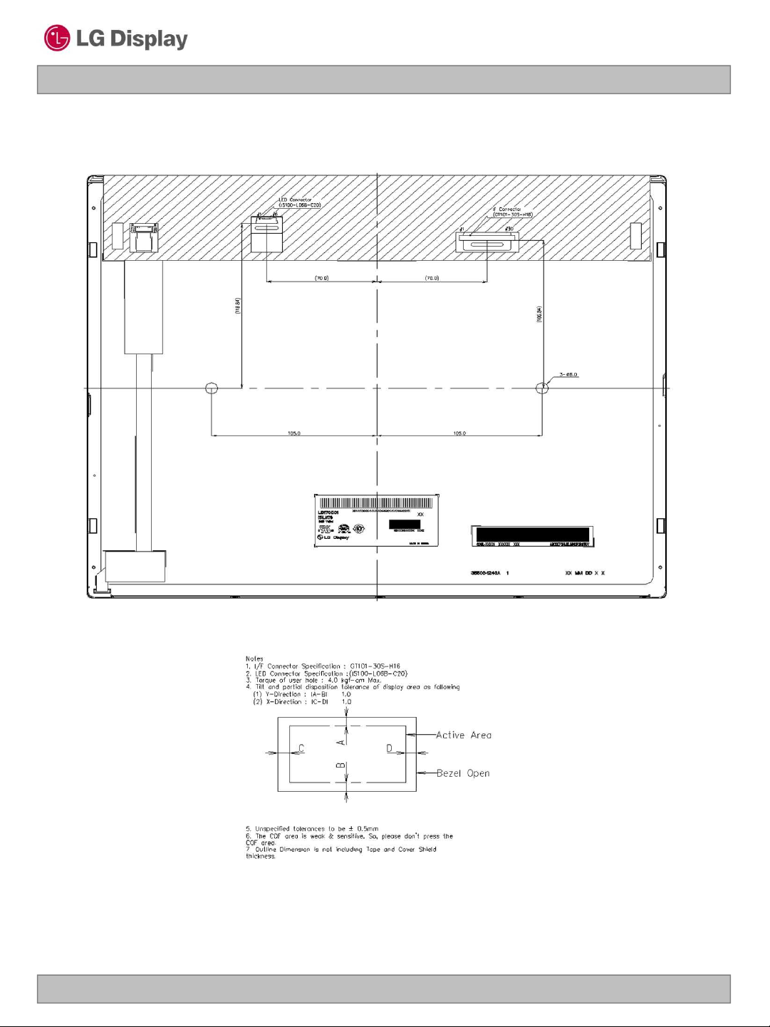
<REAR VIEW>
LB170E01-SL01
Liquid Crystal Display
Product Specification
LGD Highly recommendation :
As The IPS panel is sensitive & slim, please recommend the metal frame of the system supports the panel
by the double side-mount.
Ver. 0.3 Jun. 18. 2013
Note : This document is preliminary version. The latest version must be checked from LG Display before detail design.
26 / 31
Page 27

Product Specification
6. Reliability
Environment test condition
No Test Item Condition
LB170E01-SL01
Liquid Crystal Display
1 High temperature storage test
2 Low temperature storage test
3 High temperature operation test
4 Low temperature operation test
5
6
7 Humidity condition Operation
8
Vibration test
(non-operating)
Shock test
(non-operating)
Altitude
operating
storage / shipment
Ta= 80°C 240h
Ta= -20°C 240h
Ta= 70°C 240h
Ta= -10°C 240h
Wave form : random
Vibration level : 1.00G RMS
Bandwidth : 10-300Hz
Duration : X, Y, Z, 10 min
One time each direction
Shock level : 100G
Waveform : half sine wave, 2ms
Direction : ±X, ±Y, ±Z
One time each direction
Ta= 50 °C ,80%RH
0 - 16,000 feet(4,876m)
0 - 40,000 feet(12,192m)
Ver. 0.3 Jun. 18. 2013
Note : This document is preliminary version. The latest version must be checked from LG Display before detail design.
27 / 31
Page 28
LB170E01-SL01
Liquid Crystal Display
Product Specification
7. International Standards
7-1. Safety
a) UL 60950-1, Underwriters Laboratories Inc.
Information Technology Equipment - Safety - Part 1 : General Requirements.
b) CAN/CSA C22.2 No.60950-1-07, Canadian Standards Association.
Information Technology Equipment - Safety - Part 1 : General Requirements.
c) EN 60950-1, European Committee for Electrotechnical Standardization (CENELEC).
Information Technology Equipment - Safety - Part 1 : General Requirements.
d) IEC 60950-1, The International Electrotechnical Commission (IEC).
Information Technology Equipment - Safety - Part 1 : General Requirements.
7-2. EMC
a) ANSI C63.4 “American National Standard for Methods of Measurement of Radio-Noise
Emissions from Low-Voltage Electrical and Electronic Equipment in the Range of 9 kHz to 40 GHz.”
American National Standards Institute (ANSI), 2003.
b) CISPR 22 “Information technology equipment – Radio disturbance characteristics – Limit and
methods of measurement." International Special Committee on Radio Interference
(CISPR), 2005.
c) CISPR 13 “Sound and television broadcast receivers and associated equipment – Radio disturbance
characteristics – Limits and method of measurement." International Special Committee on Radio
Interference (CISPR), 2006.
7-3. Environment
a) RoHS. Directive 2002/95/EC of the European Parliament and of the Council on the reduction of the
use of certain hazardous substances in electrical and electronic equipment. January 2003
Ver. 0.3 Jun. 18. 2013
Note : This document is preliminary version. The latest version must be checked from LG Display before detail design.
28 / 31
Page 29

8. Packing
8-1. Designation of Lot Mark
a) Lot Mark
A B C D E F G H I J K L M
A,B,C : SIZE(INCH) D : YEAR
E : MONTH F ~ M : SERIAL NO.
Note
1. YEAR
LB170E01-SL01
Liquid Crystal Display
Product Specification
Year
Mark
CBA
2014E2015
D
201320122011
2016G2017H2018J2019
F
2. MONTH
Month
Mark
Apr5May
4
Jun
6
Jul8Aug9Sep
7
b) Location of Lot Mark
Serial No. is printed on the label. The label is attached to the backside of the LCD module.
This is subject to change without prior notice.
8-2. Packing Form
a) Package quantity in one box : 12 pcs
b) Box Size : 365 X 315 X 492mm
2020
K
Oct
A
Nov
B
DecMarFebJan
C321
Ver. 0.3 Jun. 18. 2013
Note : This document is preliminary version. The latest version must be checked from LG Display before detail design.
29 / 31
Page 30

LB170E01-SL01
Liquid Crystal Display
Product Specification
9. PRECAUTIONS
Please pay attention to the followings when you use this TFT LCD module.
9-1. MOUNTING PRECAUTIONS
(1) You must mount a module using holes arranged in four corners or four sides.
(2) You should consider the mounting structure so that uneven force (ex. Twisted stress) is not applied to the
module. And the case on which a module is mounted should have sufficient strength so that external
force is not transmitted directly to the module.
(3) Please attach the surface transparent protective plate to the surface in order to protect the polarizer.
Transparent protective plate should have sufficient strength in order to the resist external force.
(4) You should adopt radiation structure to satisfy the temperature specification.
(5) Acetic acid type and chlorine type materials for the cover case are not desirable because the former
generates corrosive gas of attacking the polarizer at high temperature and the latter causes circuit break
by electro-chemical reaction.
(6) Do not touch, push or rub the exposed polarizers with glass, tweezers or anything harder than HB
pencil lead. And please do not rub with dust clothes with chemical treatment.
Do not touch the surface of polarizer for bare hand or greasy cloth.(Some cosmetics are detrimental
to the polarizer.)
(7) When the surface becomes dusty, please wipe gently with absorbent cotton or other soft materials like
chamois soaks with petroleum benzene. Normal-hexane is recommended for cleaning the adhesives
used to attach front / rear polarizers. Do not use acetone, toluene and alcohol because they cause
chemical damage to the polarizer.
(8) Wipe off saliva or water drops as soon as possible. Their long time contact with polarizer causes
deformations and color fading.
(9) Do not open the case because inside circuits do not have sufficient strength.
(10) As The IPS panel is sensitive & slim, please recommend the metal frame of the system supports the panel
by the double side-mount.
9-2. OPERATING PRECAUTIONS
(1) The spike noise causes the mis-operation of circuits. It should be lower than following voltage :
V=±200mV(Over and under shoot voltage)
(2) Response time depends on the temperature.(In lower temperature, it becomes longer.)
(3) Brightness depends on the temperature. (In lower temperature, it becomes lower.)
And in lower temperature, response time(required time that brightness is stable after turned on) becomes
longer.
(4) Be careful for condensation at sudden temperature change. Condensation makes damage to polarizer or
electrical contacted parts. And after fading condensation, smear or spot will occur.
(5) When fixed patterns are displayed for a long time, remnant image is likely to occur.
(6) Module has high frequency circuits. Sufficient suppression to the electromagnetic interference shall be
done by system manufacturers. Grounding and shielding methods may be important to minimized the
interference.
(7) Please do not give any mechanical and/or acoustical impact to LCM. Otherwise, LCM can’t be operated
its full characteristics perfectly.
(8) A screw which is fastened up the steels should be a machine screw.
(if not, it causes metallic foreign material and deal LCM a fatal blow)
(9) Please do not set LCD on its edge.
(10) When LCMs are used for public display defects such as Yogure, image sticking can not be guarantee.
Ver. 0.3 Jun. 18. 2013
Note : This document is preliminary version. The latest version must be checked from LG Display before detail design.
30 / 31
Page 31

LB170E01-SL01
Liquid Crystal Display
Product Specification
9-3. ELECTROSTATIC DISCHARGE CONTROL
Since a module is composed of electronic circuits, it is not strong to electrostatic discharge. Make certain that
treatment persons are connected to ground through wrist band etc. And don’t touch interface pin directly.
9-4. PRECAUTIONS FOR STRONG LIGHT EXPOSURE
Strong light exposure causes degradation of polarizer and color filter.
9-5. STORAGE
When storing modules as spares for a long time, the following precautions are necessary.
(1) Store them in a dark place. Do not expose the module to sunlight or fluorescent light. Keep the temperature
between 5°C and 35°C at normal humidity.
(2) The polarizer surface should not come in contact with any other object.
It is recommended that they be stored in the container in which they were shipped.
9-6. HANDLING PRECAUTIONS FOR PROTECTION FILM
(1) The protection film is attached to the bezel with a small masking tape.
When the protection film is peeled off, static electricity is generated between the film and polarizer.
This should be peeled off slowly and carefully by people who are electrically grounded and with well ionblown equipment or in such a condition, etc.
(2) When the module with protection film attached is stored for a long time, sometimes there remains a very
small amount of glue still on the bezel after the protection film is peeled off.
(3) You can remove the glue easily. When the glue remains on the bezel surface or its vestige is recognized,
please wipe them off with absorbent cotton waste or other soft material like chamois soaked with normalhexane.
Ver. 0.3 Jun. 18. 2013
Note : This document is preliminary version. The latest version must be checked from LG Display before detail design.
31 / 31
 Loading...